Welcome to the Software
This document describes the common configuration, usage and debugging methods of the SDK, so that users can get started quickly and solve most of the problems encountered in the actual development process.
TBD
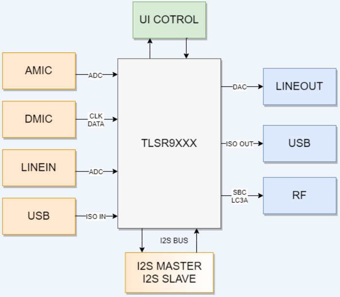
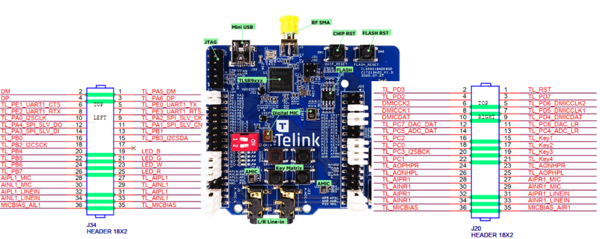
For details of EVB development board, please refer to the document "Telink TLSR9518A Generic Starter Kit Hardware Guide_internal_V1.0.pdf".
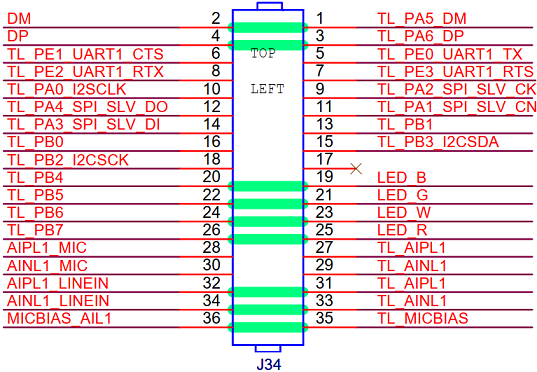
There are left and right linein inputs, which can be single-ended or differential input. EVB defaults to differential connection.
Single left linein:
Short connection:
AIPL1_LINEIN(J34_32)--TL_AIPL1(J34_31)
AINL1_LINEIN(J34_34)--TL_AINL1(J34_33)
Disconnect:
AIPL1_MIC(J34_28)--TL_AIPL1(J34_27)
AINL1_MIC(J34_30)--TL_AINL1(J34_29)
MICBIAS_AIL1(J34_36)--TL_MICBIAS(J34_35)
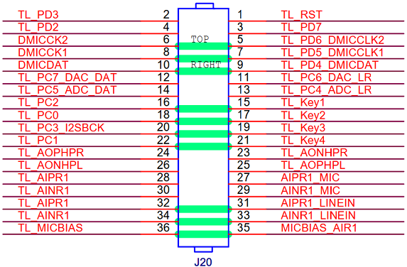
Single right linein:
Short connection:
AIPR1_LINEIN(J20_32)--TL_AIPR1(J20_31)
AIPR1_LINEIN(J20_34)--TL_AINL1(J20_33)
Disconnect:
AIPR1_MIC(J20_28)--TL_AIPR1(J20_27)
AINR1_MIC(J20_30)--TL_AINR1(J20_29)
MICBIAS_AIR1(J20_36)--TL_MICBIAS(J20_35)
There are left and right amic inputs, which can be single-ended or differential input. EVB defaults to differential connection.
Single left amic:
Short connection:
AIPL1_MIC(J34_28)--TL_AIPL1(J34_27)
AINL1_MIC(J34_30)--TL_AINL1(J34_29)
MICBIAS_AIL1(J34_36)--TL_MICBIAS(J34_35)
Disconnect:
AIPL1_LINEIN(J34_32)--TL_AIPL1(J34_31)
AINL1_LINEIN(J34_34)--TL_AINL1(J34_33)
Single right amic:
Short connection:
AIPR1_MIC(J20_28)--TL_AIPR1(J20_27)
AINR1_MIC(J20_30)--TL_AINR1(J20_29)
MICBIAS_AIR1(J20_36)--TL_MICBIAS(J20_35)
Disconnect:
AIPR1_LINEIN(J20_32)--TL_AIPR1(J20_31)
AIPR1_LINEIN(J20_34)--TL_AINL1(J20_33)
DMIC only needs 2 signal lines data and clk, and the clk frequency fixed at 3 MHz.
Dual DMIC has 1 signal line data and 2 clk, dual dmic share data, 2 clk timing is the same, in the clk rising edge to collect one dmic data, in the clk falling edge to collect the other dmic data.
Short connection:
Left and right mic shared data: DMICDAT(J20-10)-- TL_PD4_DMICDAT(J20-9)
Left mic: DMICCK1(J20-8)--TL_PD6_DMICCLK1(J20-7)
Right mic: DMICCK2(J20-6)--TL_PD6_DMICCLK2(J20-5)
Short connection:
DM(J34-2)--TL_PA5_DM (J34-1)
DP(J34-4)--TL_PA6_DP (J34-3)
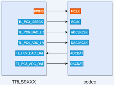
I2S Master-Slave mode is supported, but it is recommended that the TRLS9XXX I2S be the Master, as the Master does not need to do asynchronous resampling, which reduces computing power consumption.
Three EVB boards and three USB cables are required.
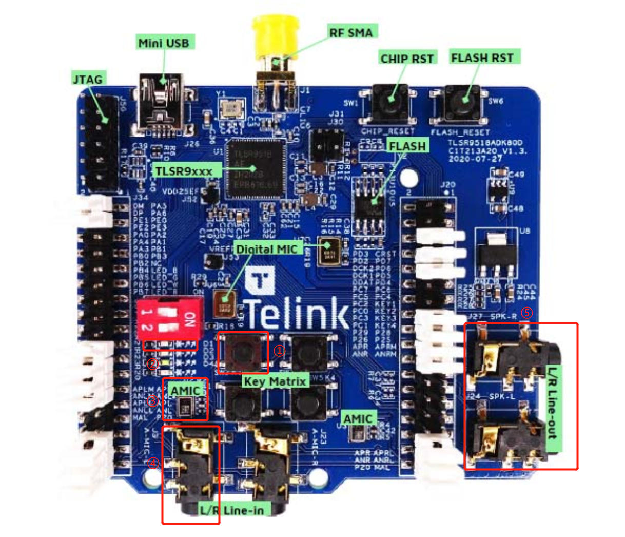
Description:
Pairing button: short press to enter the pairing state, double-click to exit the pairing state.
Connection status indicator: fast flashing for pairing status, slow flashing for reconnection status, constant light for connection status.
As shown in the figure above, the L Linein input and Lineout output interface are used. If the analog mic is used as the input, the Tx port J34 needs to be short connected as shown in the red box in the figure below.
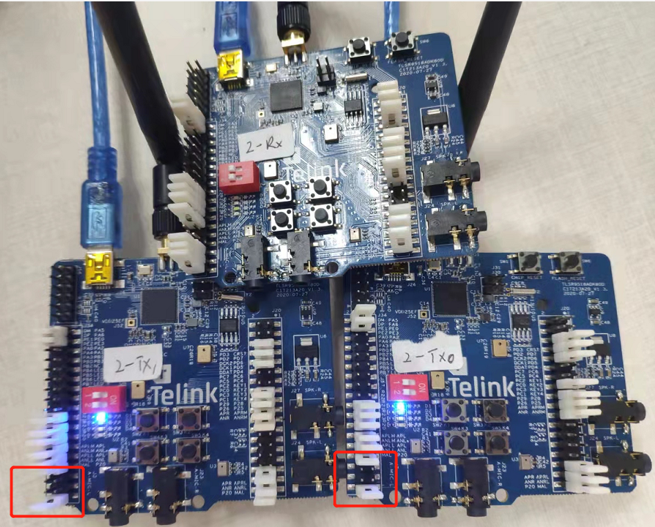
Two EVB as TX to burn _img_proj_ultra_ll_mictx.bin, one EVB as RX to burn _img_proj_ultra_ll_micrx.bin (the firmware is in the release_bin directory), the burning procedure is as follows:
Step 1: Prepare the Telink burner and connect it as shown in the figure below.
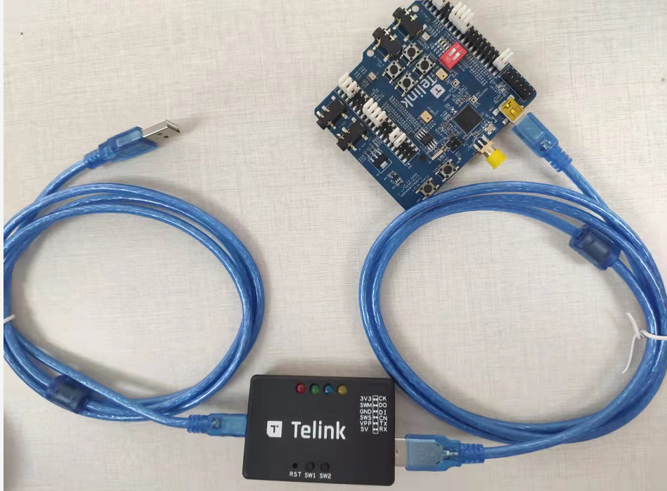
Step 2: Open the Telink BDT.exe program.
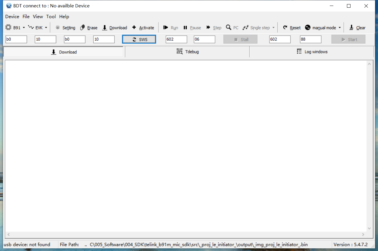
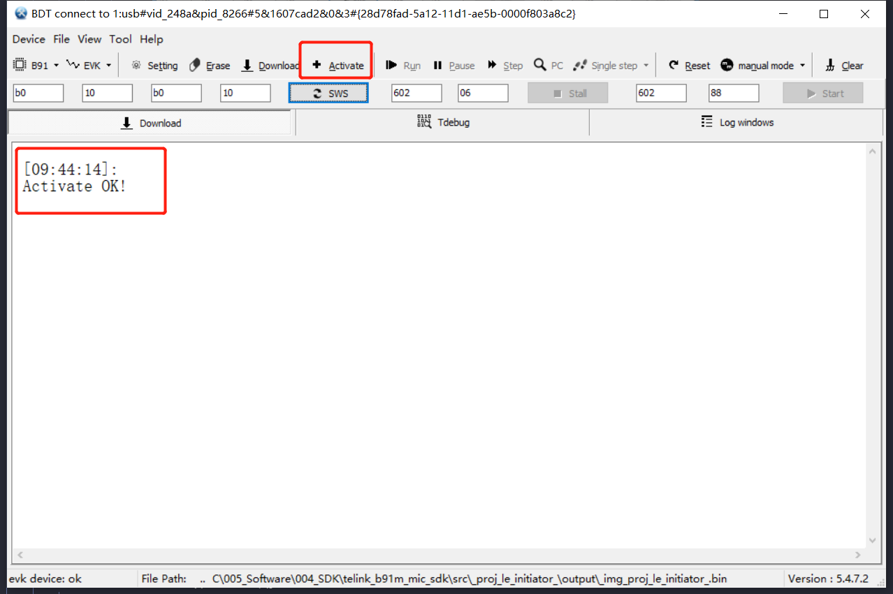
Step 3: Click "Activate".
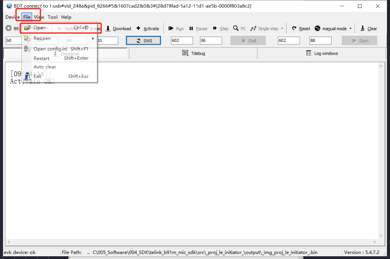
Step 4: Click "File", and click "Open" in the drop-down menu.
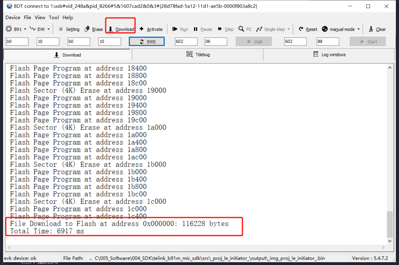
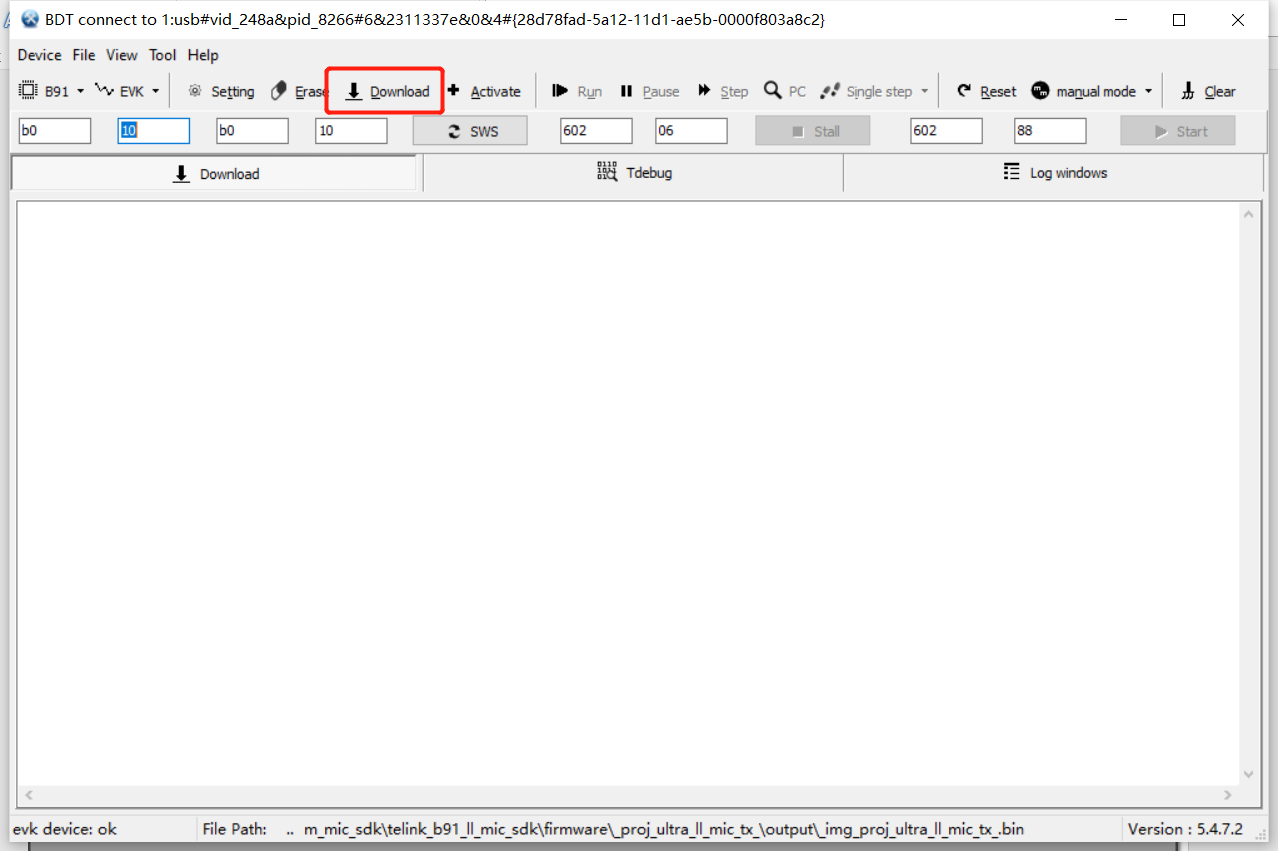
Select the firmware to be burned, and then click "Download", as shown below:
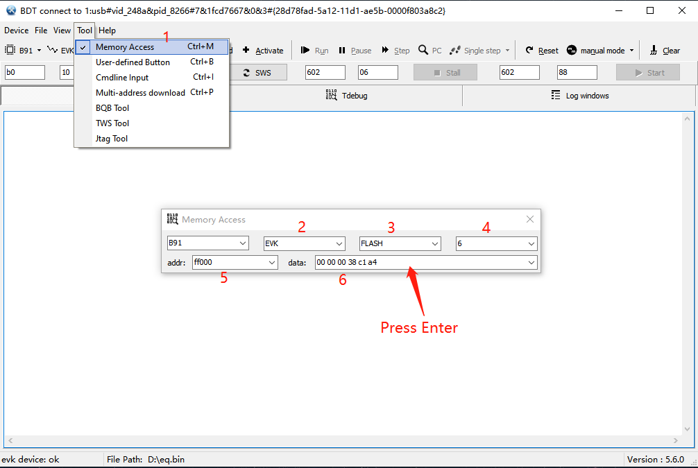
Step 5: Burn the MAC address, open "Memory Access", operate and fill in the MAC address in the order of the numbers in the figure below, if you want to burn the MAC address as: 0xa4c138000000, then fill in: 00 00 00 38 c1 a4, as shown below, after filling in, press "Enter" to burn it. (For more operations of the BDT tool, you can visit: http://wiki.telink-semi.cn/wiki/IDE-and-Tools/Burning-and-Debugging-Tools-for-all-Series/)
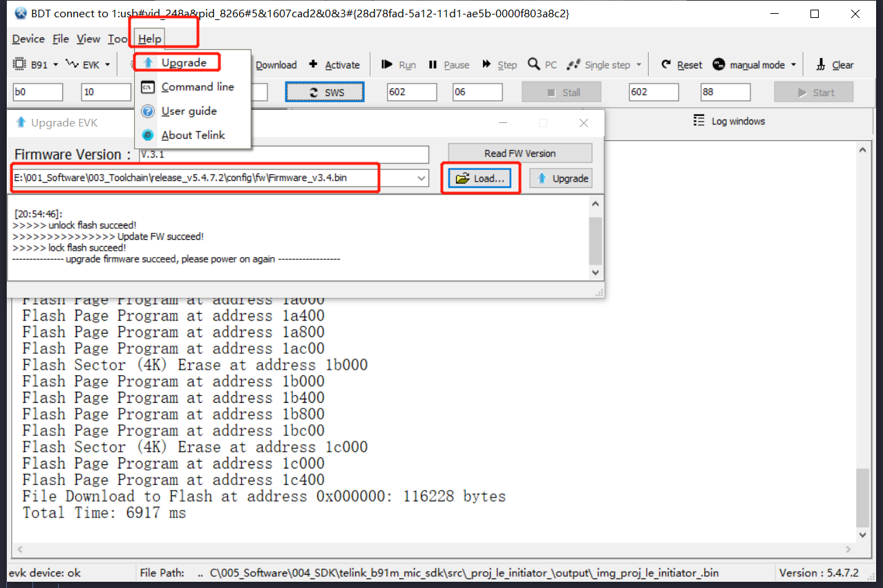
Note that when the burner fails to activate, you need to upgrade the firmware of the burner, as shown below, click "Help", select "Upgrade", load the firmware under the burning software path, finally unplug and re-plug the burner.
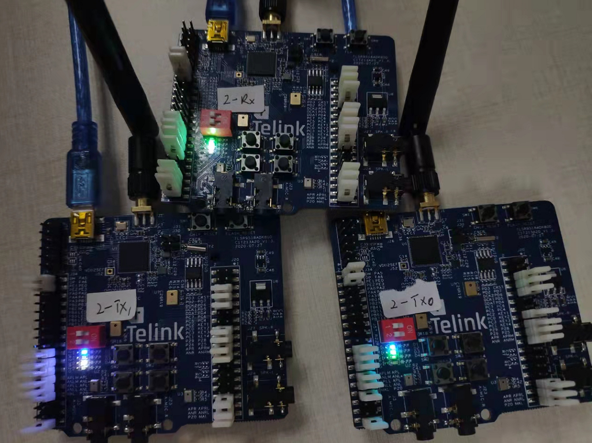
After powering on again, short press TX0 and SW2 button on RX to pair TX0; then press TX1 and SW2 button on RX to pair TX2. After the pairing is successful, while the blue lights of TX0 and TX1 are always on, they will light up the green and white lights of the channel respectively, while the Rx will light up the green and white lights at the same time, as shown in the figure:
Finally, the audio can be monitored through the Lineout interface. Note: Lineout on the Tx end outputs the audio encoded by the local AMIC /uploads/zip/20230213112102661G2/pickup audio and then decoded, while Lineout on the Rx end outputs the audio decoded from the encoded audio data sent from the remote Tx0 and Tx1 respectively.
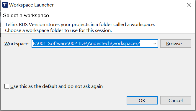
When you first open the Andesight IDE, a dialog box for selecting workspace will pop up, you need to click "Browse..." to select a directory as your workspace, any directory can be selected as the workspace directory.
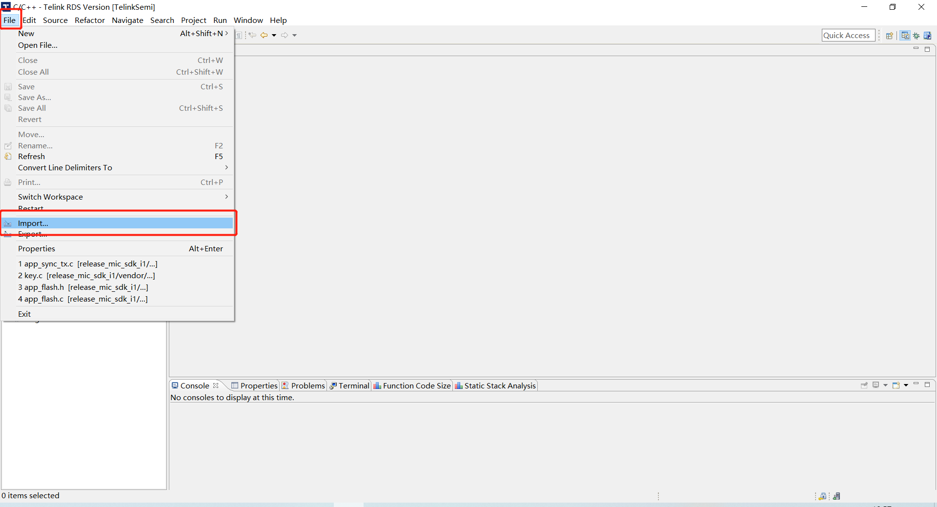
Select "File -> Import", as shown below.
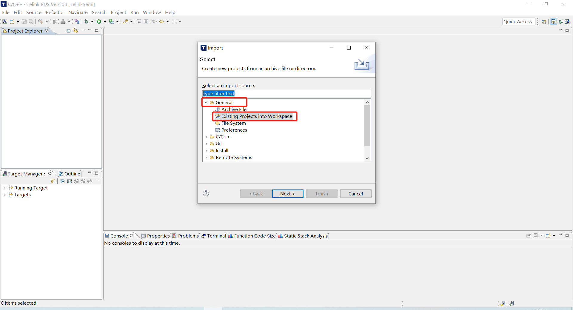
In the pop-up window, click "General" and select "Existing Projects into Workspace".
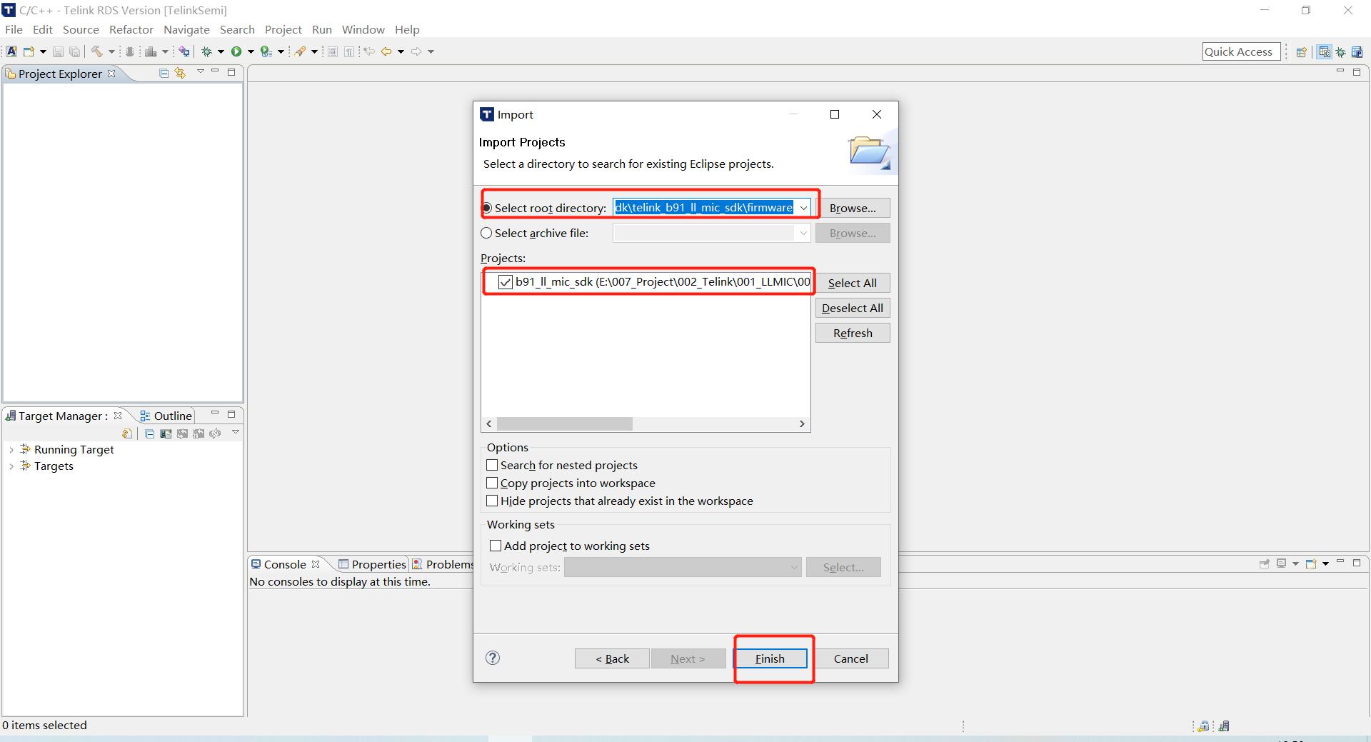
Enter the path to the SDK in the "Select root directory" box, or click "Browser" directly and select the directory where the SDK is located, then tick the SDK and click "Finish" to import the project. (Note: It is recommended to distinguish between the IDE working path and the path where the SDK source code is located, so as to facilitate the opening of multiple projects.)
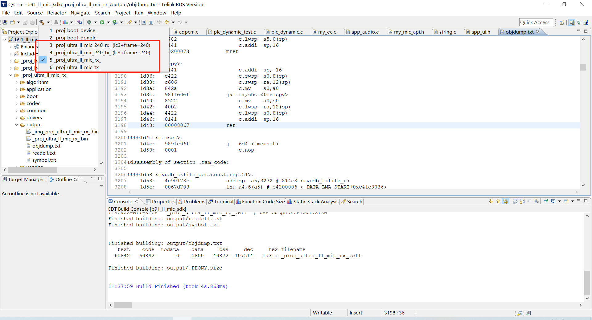
Before compiling the project, you need to click on the corresponding project, and first compile the two projects _proj_bootdevice and _proj_bootdongle for subsequent generation of merged firmware.
Note:
When compiling for the first time, you must compile two boot projects first, and then compile the main project, otherwise an error will be reported.

Then compile the 3(receiver), 4(transmitter) or 5(receiver), 6(transmitter) projects.
The full name of Telink BDT tool is "Telink Burning and Debugging Tool". For specific functions, please refer to the "Tool User Guide" document. Several common application scenarios are listed below.
Telink BDT is based on TWS and implements the function of burning multiple bin files, and is also applicable to this SDK. It is used as follows:
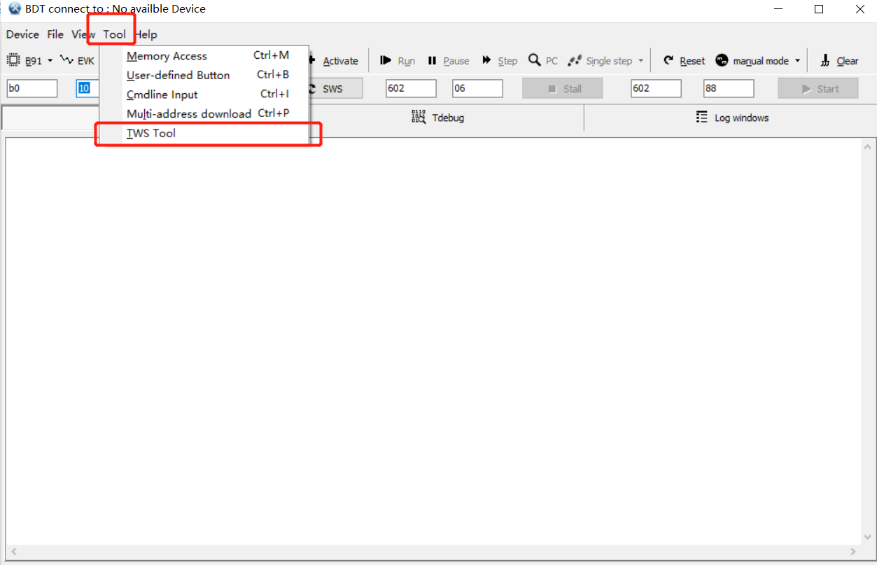
Step 1: Click "Tool", and select "TWS Tool" in the drop-down menu.
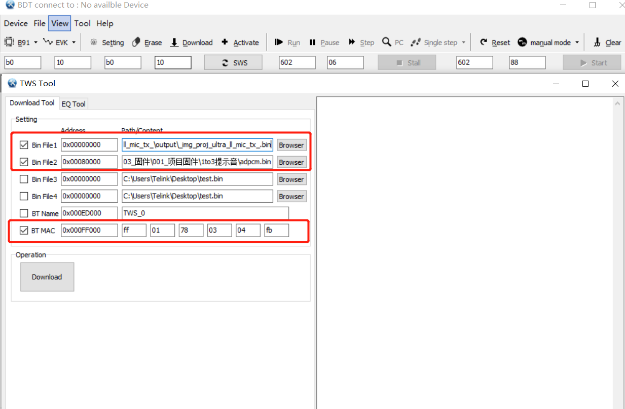
Step 2: Select the "Download Tool" page, check Bin File1, Bin File2 and BT MAC respectively, and select the corresponding project firmware, tone file and fill in the MAC address, click "Download" to burn the program, tone and MAC address at the same time.
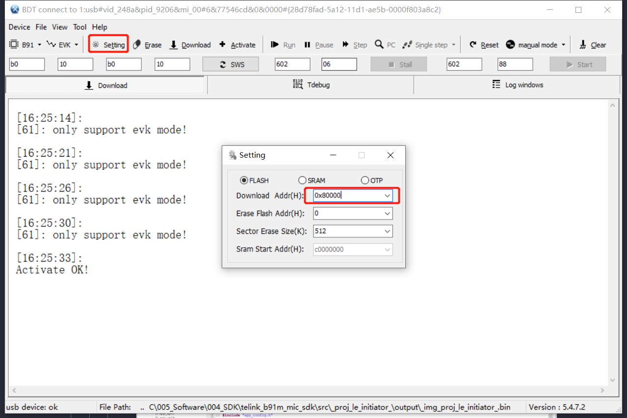
The SDK supports the tone function by default requires the tone file to be burned in the specified address. The detailed steps are as follows:
Step 1: Open Telink BDT, click "Setting", and enter 0x80000 at "Download Addr" in the pop-up window.
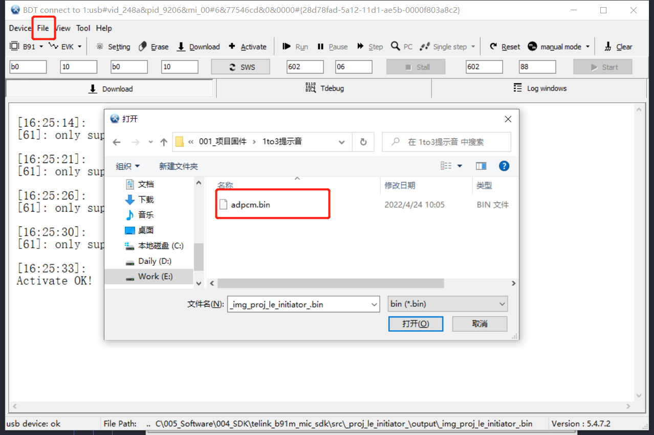
Step 2: Select 48k ADPCM tone file.
Step 3: Click "Download" to burn the tone.
Interference may occur when the MAC addresses of the two Tx ends are the same, so the MAC address can be read and written through Telink BDT.
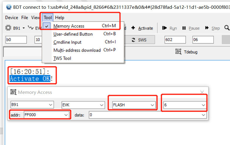
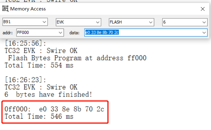
Step 1: Open Telink BDT, click "Activate", and in the case of Activate OK, click "Tool", select "Memory Access", and in the pop-up window select "Flash" for the memory type, enter "6" for the size and "FF000" for the addr.
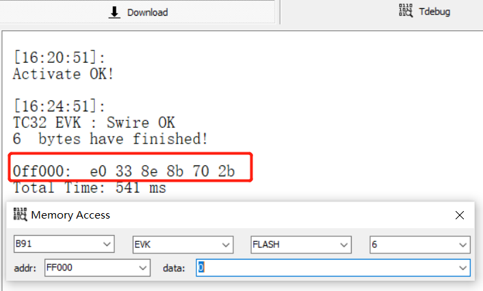
Then press the "tab" key to read the mac address stored at this address: e0 33 8e 8b 70 2b.
Step 2: Enter the mac address to be modified in the data column: e0 33 8e 8b 70 2c, and press "Enter" to write.
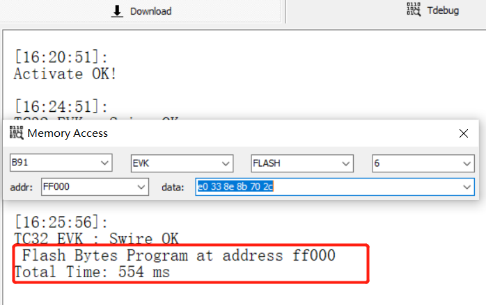
Press the "tab" key again to read the address data and find that the writing is successful:
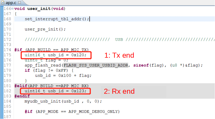
In 2-to-1 mode, the default start address of the TX end is 0x120 (determined by the 0x7FFF0 address where FLASH_SYS_USER_USBID_ADDR is located).
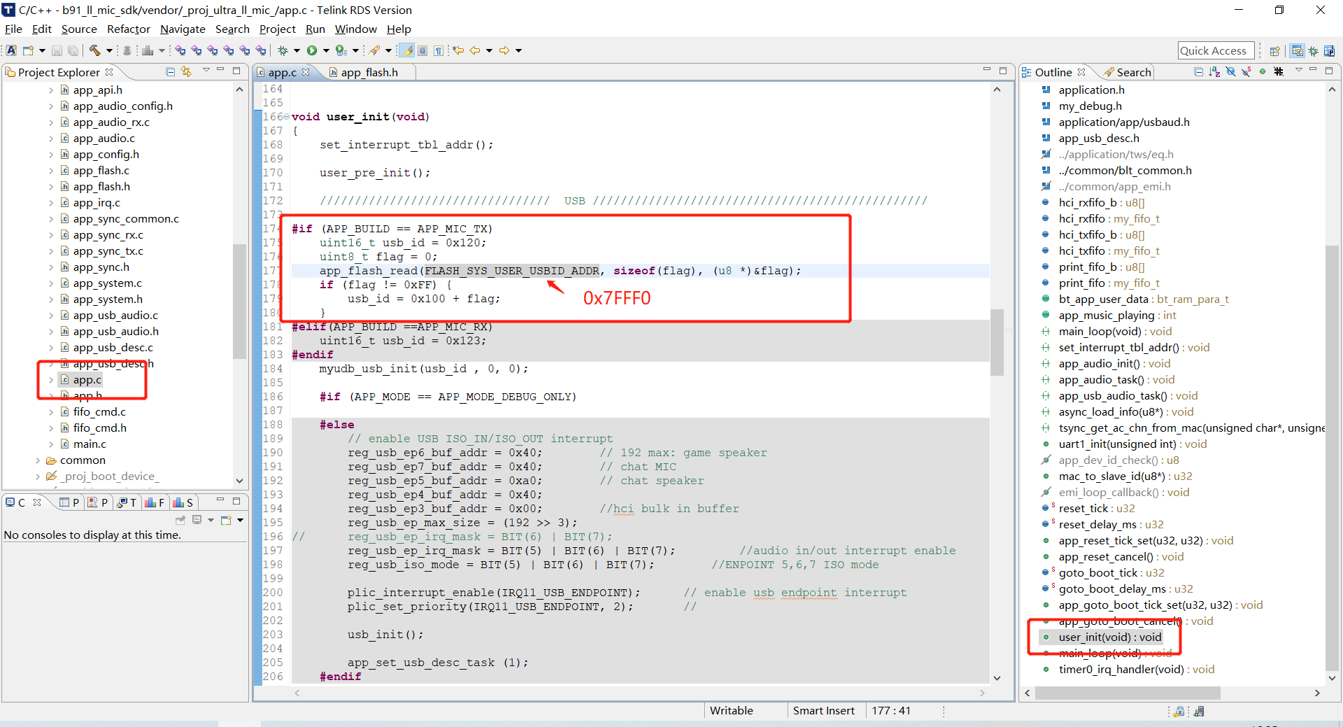
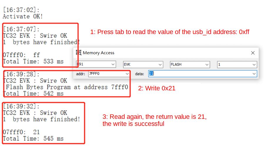
If you need to view multiple TX logs, you need to modify the usb_id addresses of the different TX to distinguish them, so as to be consistent with the pid configuration of the risc_v_tdb tool.
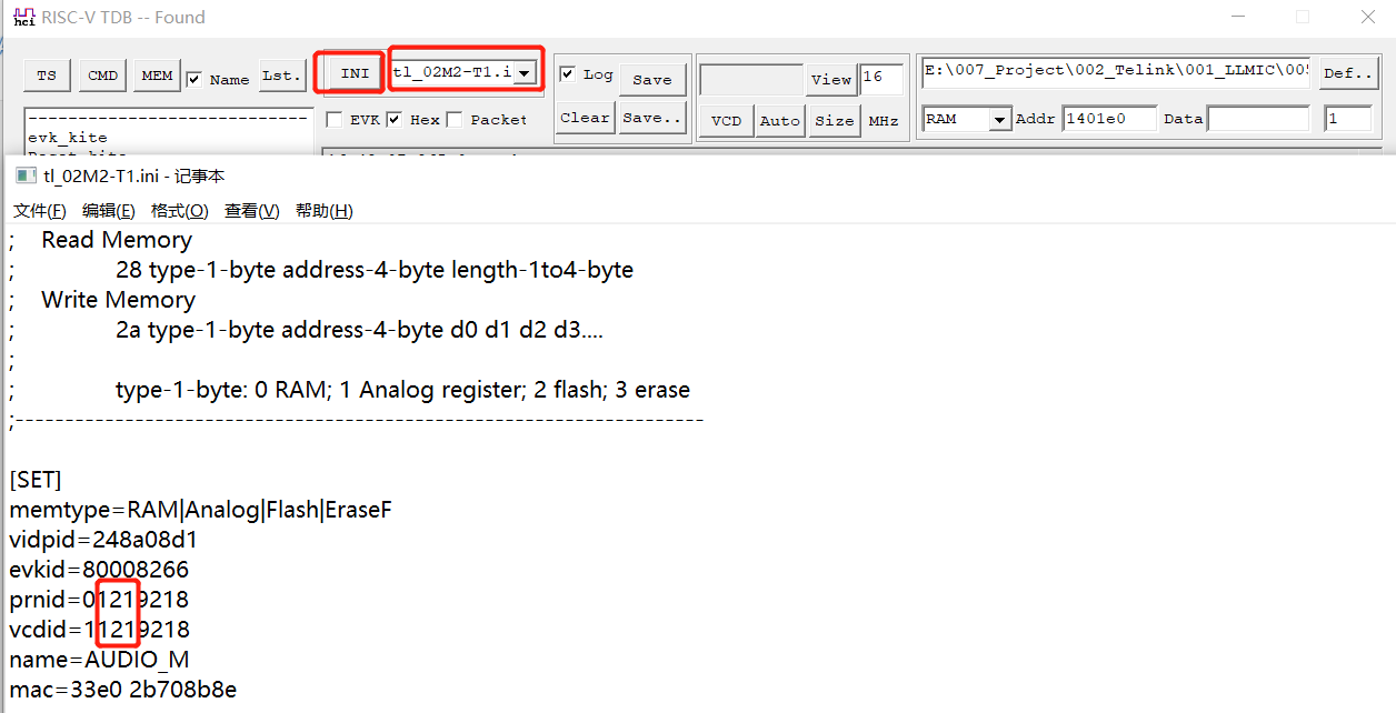
Then synchronise the corresponding values in the pid configuration of the risc_v_tdb tool.
The USB print log can use the following function, the parameter str is the string to be printed, ph is the data to be printed, and n is the length of byte. If you only need to print the string or data, you can write 0 for the unneeded parameter.
void usb_send_str_data (char *str, u8 *ph, int n);This function has commonly used encapsulation as follows:
void usb_send_str_data (char *str, u8 *ph, int n)
int usb_send_str_int (char *str,int w);
void usb_send_str_u32s (char *str, u32 d0, u32 d1, u32 d2, u32 d3);
#define my_dump_str_data(en,s,p,n)
#define my_dump_str_u32s(en,s,d0,d1,d2,d3)
Developers can call the functions.
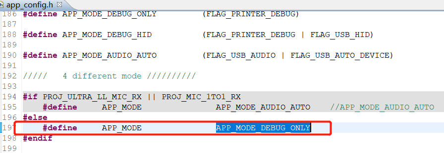
To support USB printing, you first need to configure APP_MODE to APP_MODE_DEBUG_ONLY or APP_MODE_DEBUG_HID. (In APP_MODE_AUDIO_AUTO mode you cannot use risc_v_tdb tool to view log, need to use USB to serial port tool.)
Then open different configurations according to different pids. The default pid in the Tx end is 0x1209218, and the default pid in the Rx end is 0x1239218, which consists of usb_id and pid.
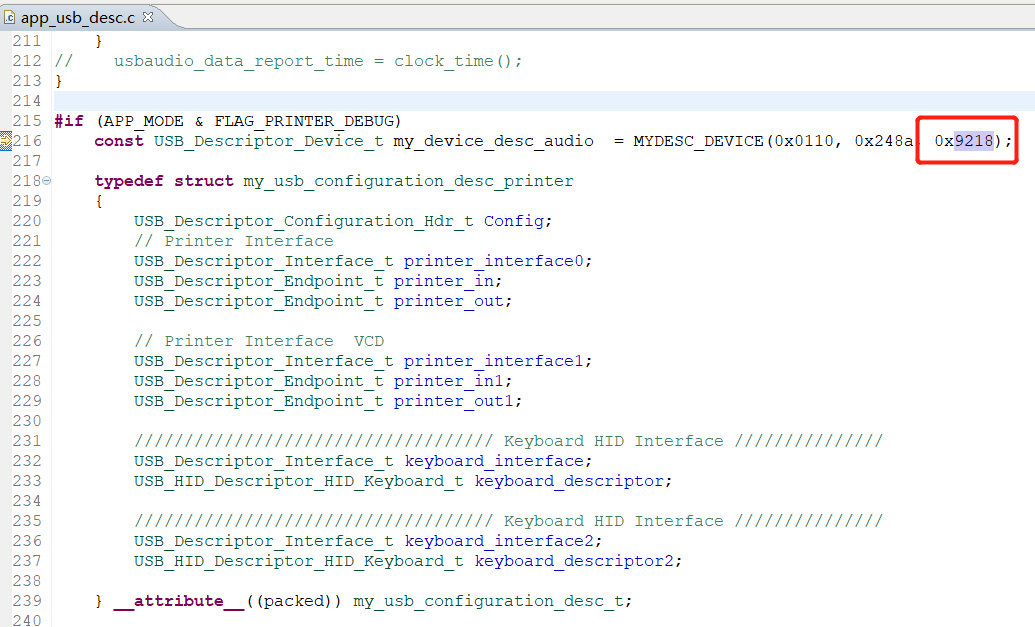
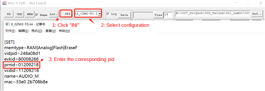
Then create different configurations according to different pids, namely Tx0, Tx1 and Rx.
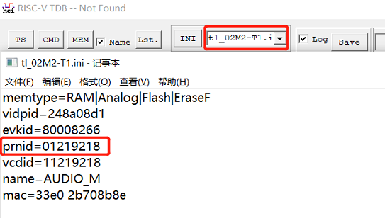
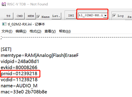
(1) risc_v_tdb supports the function of online flash writing, so as to realize the requirement of direct online upgrade program during the debugging process:
Step 1: Select the corresponding configuration, after the connection is successful, click "In File" and select the firmware to be upgraded. (Note: Before writing the firmware, the MAC address can be modified synchronously by modifying the MAC option box.)
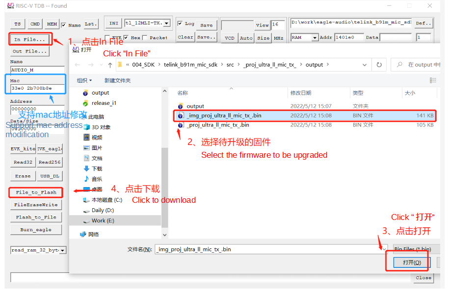
Step 2: Click "File_to_Flash" to write the firmware.
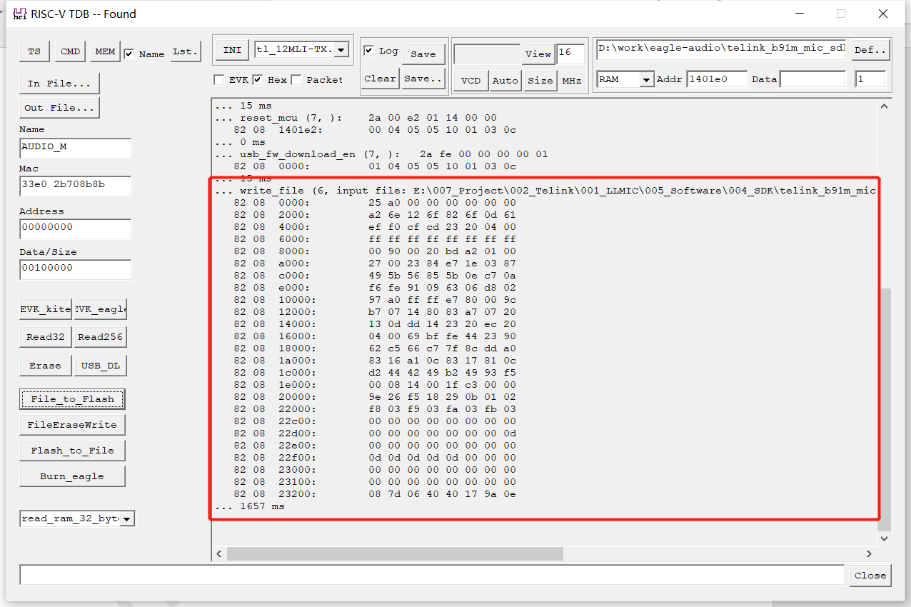
(2) risc_v_tdb also supports the function of reading flash and saving it as a file:
Step 1: Select the configuration that supports reading flash and saving it as a file.
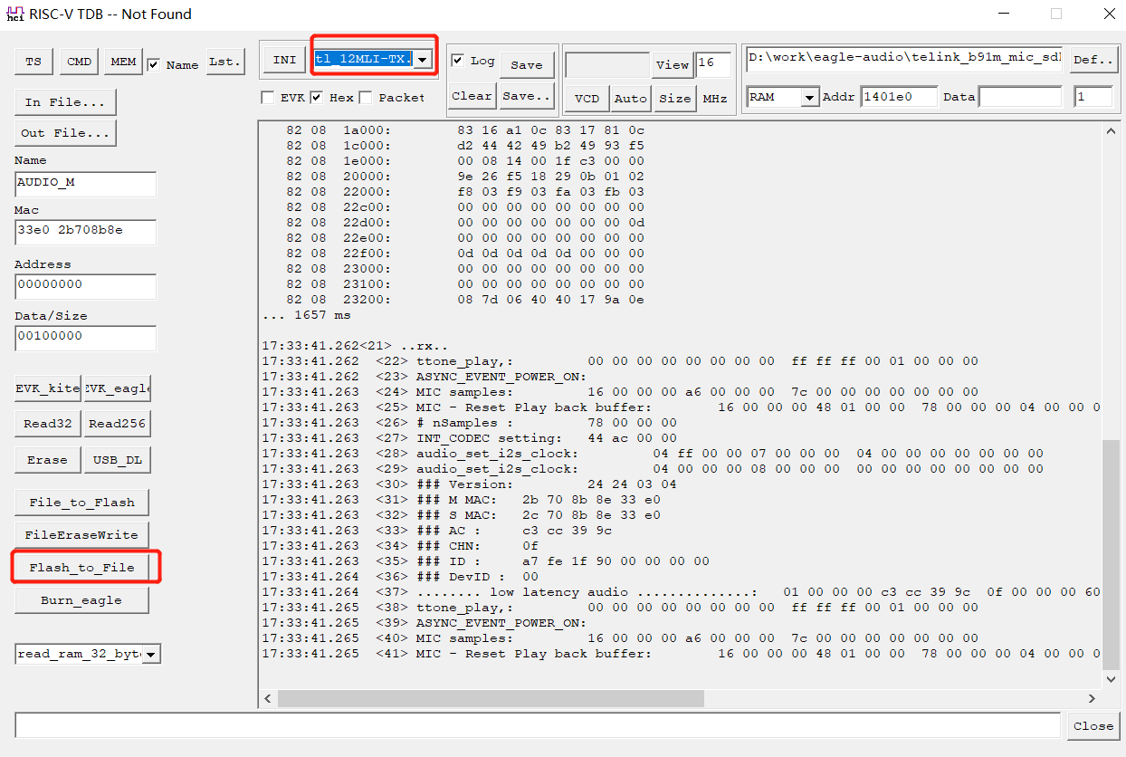
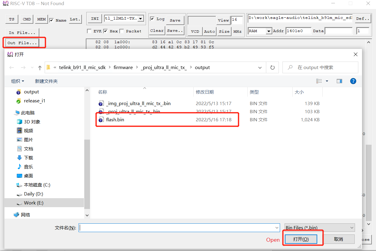
Step 2: Click "Out File", select the bin file to be written to flash.
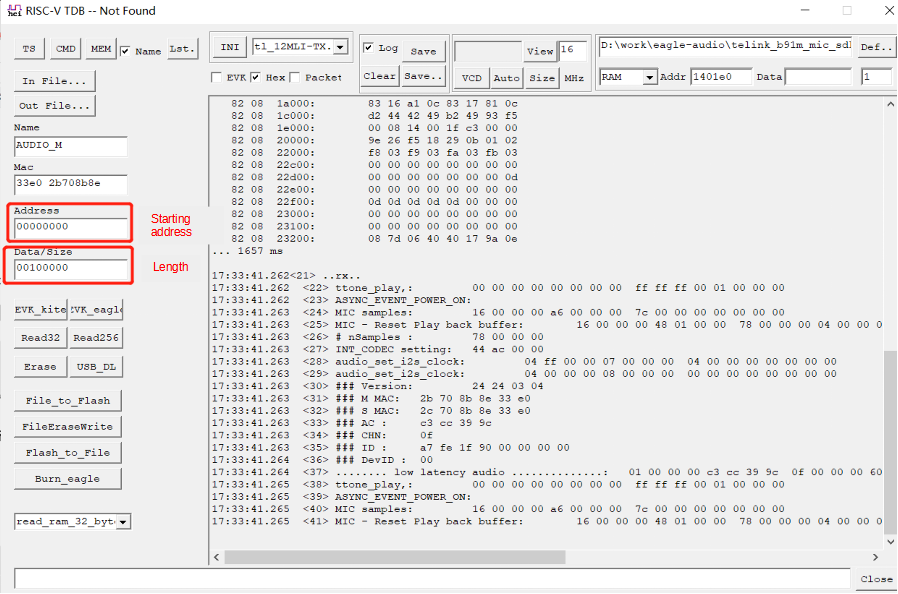
Step 3: Enter the start address of the flash to be read and the read length.
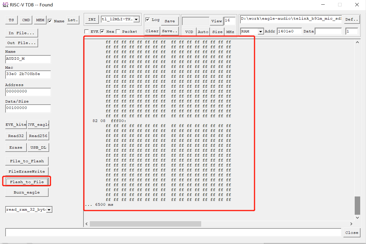
Step 4: Click "Flash_to_File" to save the read flash to the bin file.
The risc_v_tdb supports the function of sending commands to control the program: based on the USB Print mode, users can add the control function of the project in the my_usb_audio_debug interface. The currently supported functions are: pairing test control, EMI test control, tone test control, data transmission test control, and noise reduction function test control.
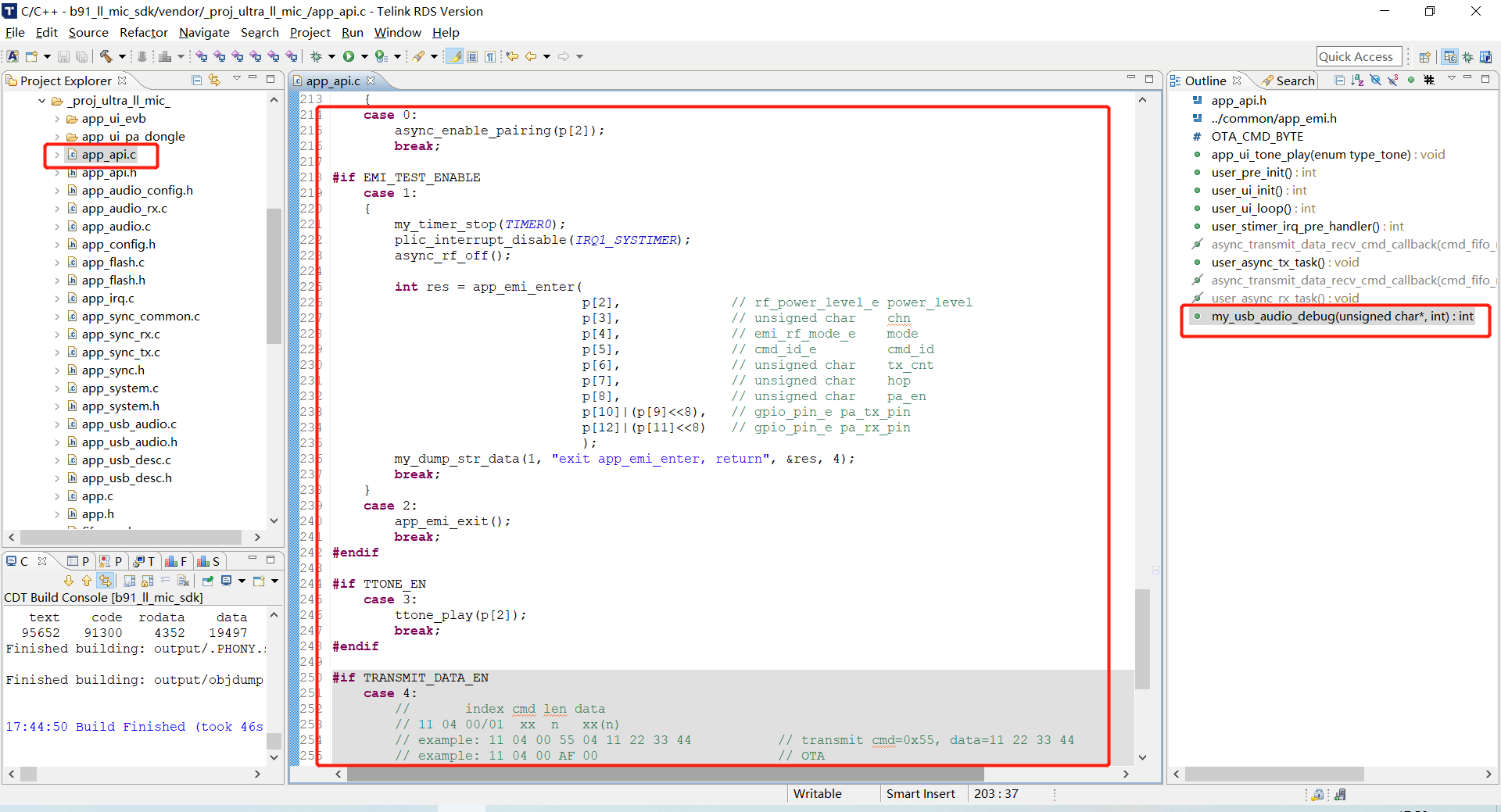
The detailed control methods are as follows:
Step 1: Use risc_v_tdb to connect to the board, and open the the corresponding macros for function configuration, such as: EMI_TEST_ENABLE, TTONE_EN, TRANSMIT_DATA_EN, APP_NS_ENABLE, etc.
Step 2: Enter the corresponding command in the command box, such as 11 00 20, and press "Enter".

Among them, 11 is the command header, 00 is the corresponding value for the pairing test control and 20 is the pairing test incoming parameter. Other test controls are the same as above.
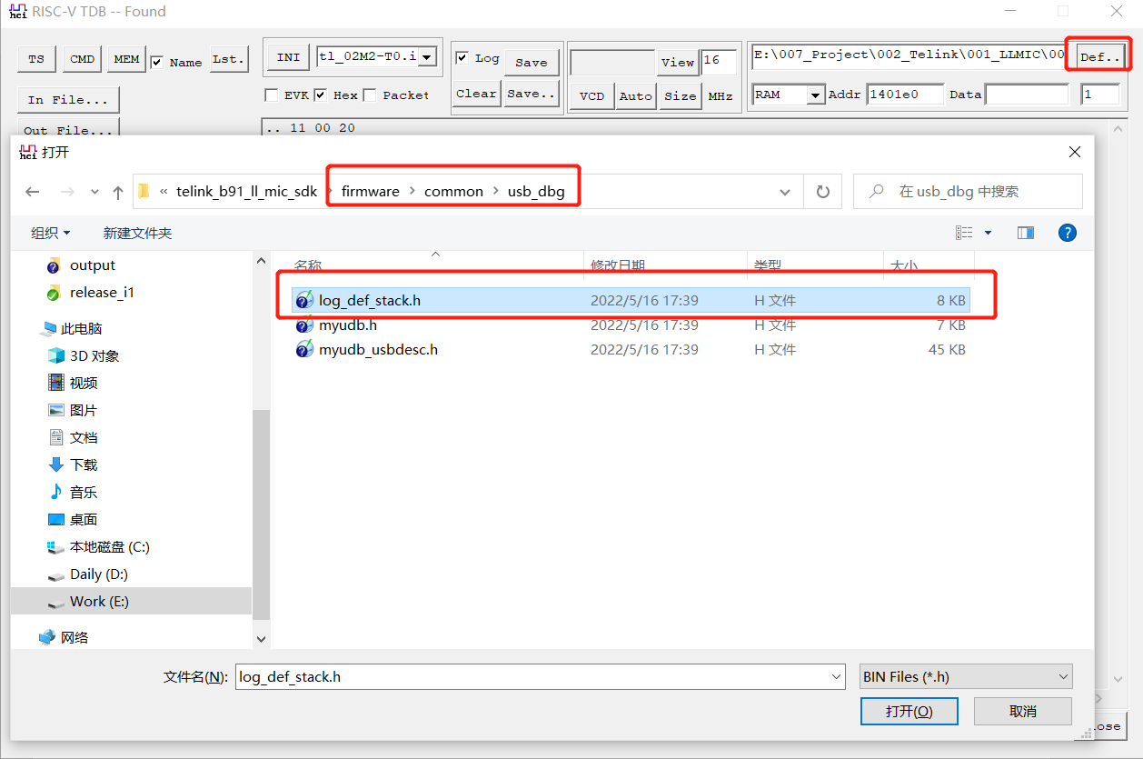
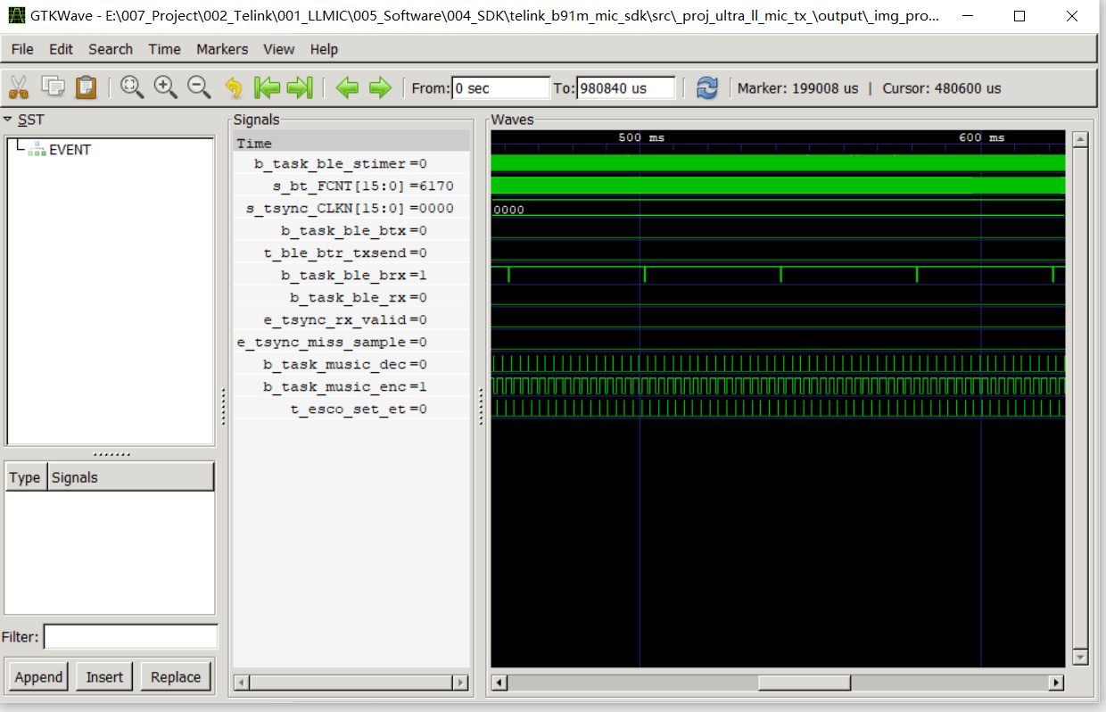
The risc_v_tdb supports the vcd waveform viewing function of Telink's own protocol, and we can view the execution of each function. The specific viewing steps are as follows:
Step 1: When connected, click "Def" and select the log_def_stack.h file in the common\usb_dbg path.
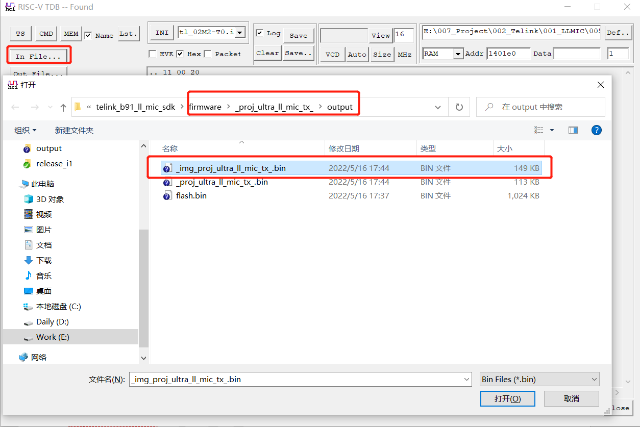
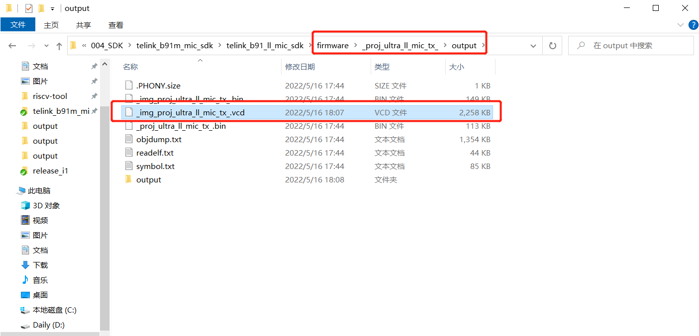
Step 2: Click "In File", select the firmware generated in the firmware\_proj_ultra_ll_mictx\output path (take _proj_ultra_ll_mictx as an example).
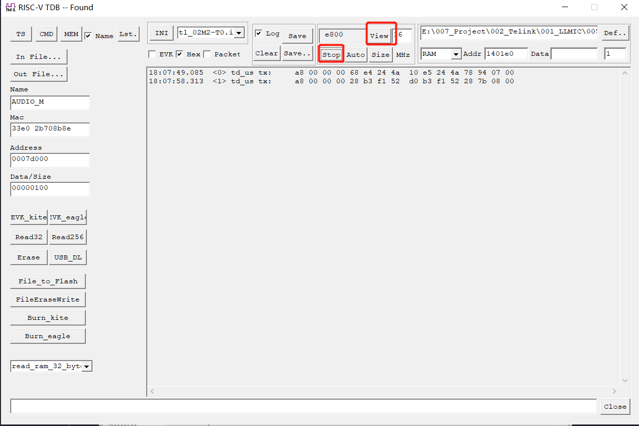
Step 3: Click "VCD" to collect:
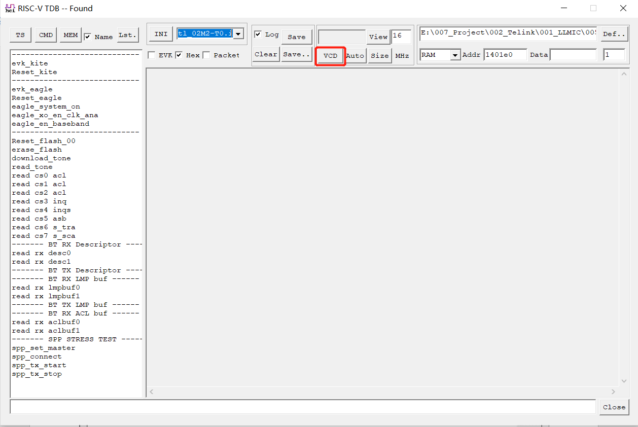
After collecting a certain amount, click "Stop", and the vcd file will be automatically saved to the output folder corresponding to the project.
Then click "View" to jump to the waveform viewing tool.
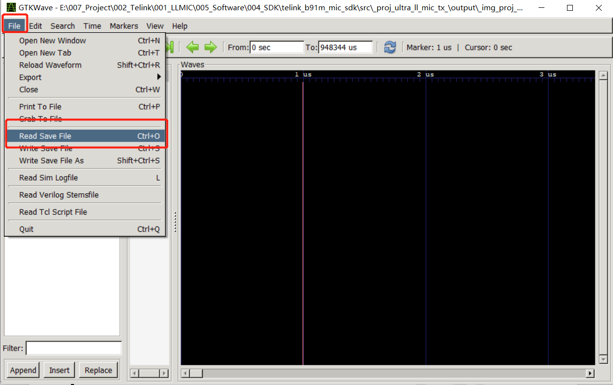
Step 4: In the pop-up tool, click "File" and select "Read Save File".
Select the mic-i1.gtkw file (in the document, the editor directly stores it in the riscv-tool root directory, this file is used to add the waveform to be viewed to the Waves window, and the user can also manually drag the desired signal to view).
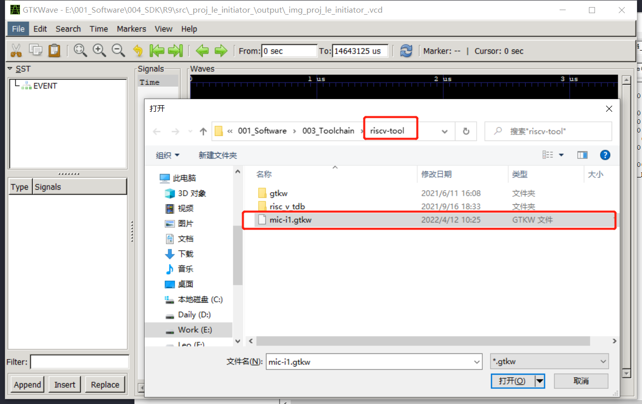
The waveform can be seen as shown in the figure below.
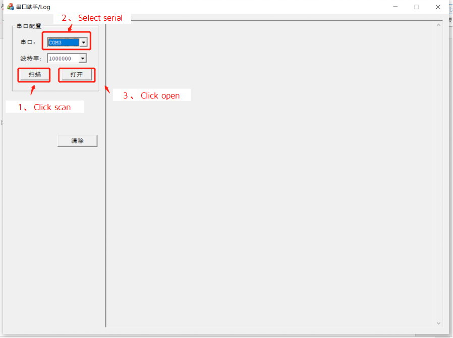
When APP_MODE is configured as APP_MODE_AUDIO_AUTO, the risc_v_tdb tool cannot be used to view the log. At this time, you need to use the usb to serial tool to view it.
Use the USB to serial tool to connect the board and PC, open the usb to serial tool TL_UART_Log_Tool, click "scan", select the corresponding serial port, click "open" to view the log. The default in the SDK is PE0 output log.
The OTA function is implemented in the BootLoader. After the chip is powered on, the BootLoader program is first executed. The main process of the BootLoader program is as follows:
(1) Read the value of the analog register 0x3c (set to: areg_v_0x3c, power on after power off, the value of areg_v_0x3c is 0x00).
(2) Determine if areg_v_0x3c is equal to 0x4b. If not, verify APP code, if verification is successful, then execute APP code.
(3) Initialize functional modules such as USB and RF, and run BootLoader function.
Method 1: There is a USB port in the RX side and no USB port in the TX side. You can use the combination Dongle+RX, Device+TX, send commands via button or USB HID or other interface to let TX and RX enter the BootLoader at the same time, and RX connect to PC via USB. The host computer can communicate and upgrade RX through USB, and can upgrade TX through RX.
Method 2: Both TX and RX have no USB interface. You can use the combination Device+RX, Device+TX, and make an upgrade board (EVB board available) to burn Dongle firmware. When the Dongle is powered on, TX or RX can receive commands through the button/serial port, jump to the BootLoader (Device), the Dongle will automatically connect to the Device, and perform OTA upgrades for the TX and RX respectively through the host computer.
The SDK defaults RX as Dongle and TX as Device. It can be changed by modifying the SDK project settings. As shown in the figure below, the TX end as the Device, If you want to use the TX as the Dongle device, you only need to change the red box in the figure below to "_proj_bootdongle\output\_proj_bootdongle".

(1) Compile _proj_bootdevice and _proj_bootdongle projects.
(2) Open the vendor/_proj_low_latency_mic/app_ui_EVB/app_ui.h file, find the TRANSMIT_DATA_EN macro (create one if not), set it to 1, and compile and burn TX and RX respectively.
(3) Open two RISC-V-TDB tools and select the corresponding ini configuration files respectively, if there is no corresponding ini file, select an ini file, click the "INI" button, and modify the prnid and vcdid of TX and RX. TX's prnid=01209218, vcdid=11209218; RX's prnid=01239218, vcdid=11239218. After setting, re-select the ini file, "RISC-V-TDB -- Found" appears in the title bar, and the following log appears, indicating that the setting is correct.
![]()
(4) Press SW2 of TX and RX at the same time to enable pairing. After successful pairing, the green or white lights of TX and RX will light up at the same time, indicating that the connection is successful.
(5) As shown above, if the green lights of TX and RX are on, at the bottom of the RISC-V-TDB tool corresponding to RX, enter the command 11 05 00, if the white lights are on, enter the command 11 05 01, press "Enter" to send the command, after 1 second TX and RX enter the BootLoader separately.
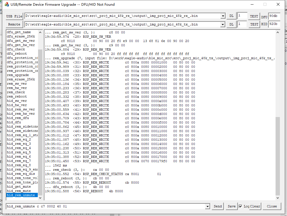
(6) Open the usb_ota.exe tool, the tool title bar displays DFU Found, indicating that the Dongle has been successfully identified. As shown in the figure below, "Remote Device Connected" appears, indicating that the Dongle and Device are successfully connected.
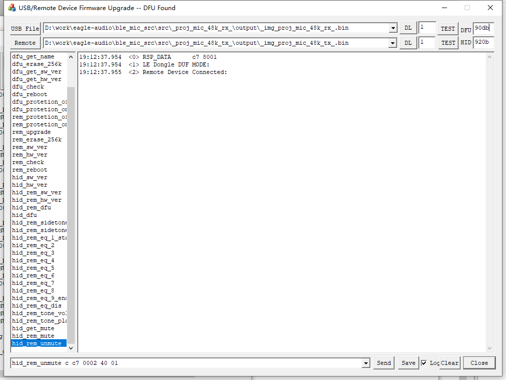
(7) Upgrade Dongle via USB interface:
a) Click the "USB File" button, and in the pop-up file selection box, select the firmware to be upgraded corresponding to Dongle.
b) Click the corresponding "DL" button on the right, and the following log will appear, indicating that the Dongle upgrade is successful.
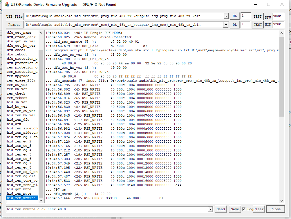
(8) Upgrade the Device through the USB interface:
a) Click the "Remote" button, and in the pop-up file selection box, select the firmware to be upgraded corresponding to the Device.
b) Click the corresponding "DL" button to the right of the "Remote" button, and the following log will appear, indicating that the Device upgrade is successful. After the Device upgrade is successful, both Dongle and Device will restart.
(9) To upgrade another TX (TX2):
a) Burn the firmware to TX2 and reset it.
b) Re-execute step 4.
EMI test tool introduction: based on USB HID, you need to configure APP_MODE to APP_MODE_DEBUG_HID (the editor uses this mode here, so as to combine with log to explain) or APP_MODE_AUDIO_AUTO, while enabling the EMI_TEST_ENABLE macro to enable the EMI test function.
Step 1: Open the emi_test_hid_tool tool and display USB Connected, which means the connection is successful.
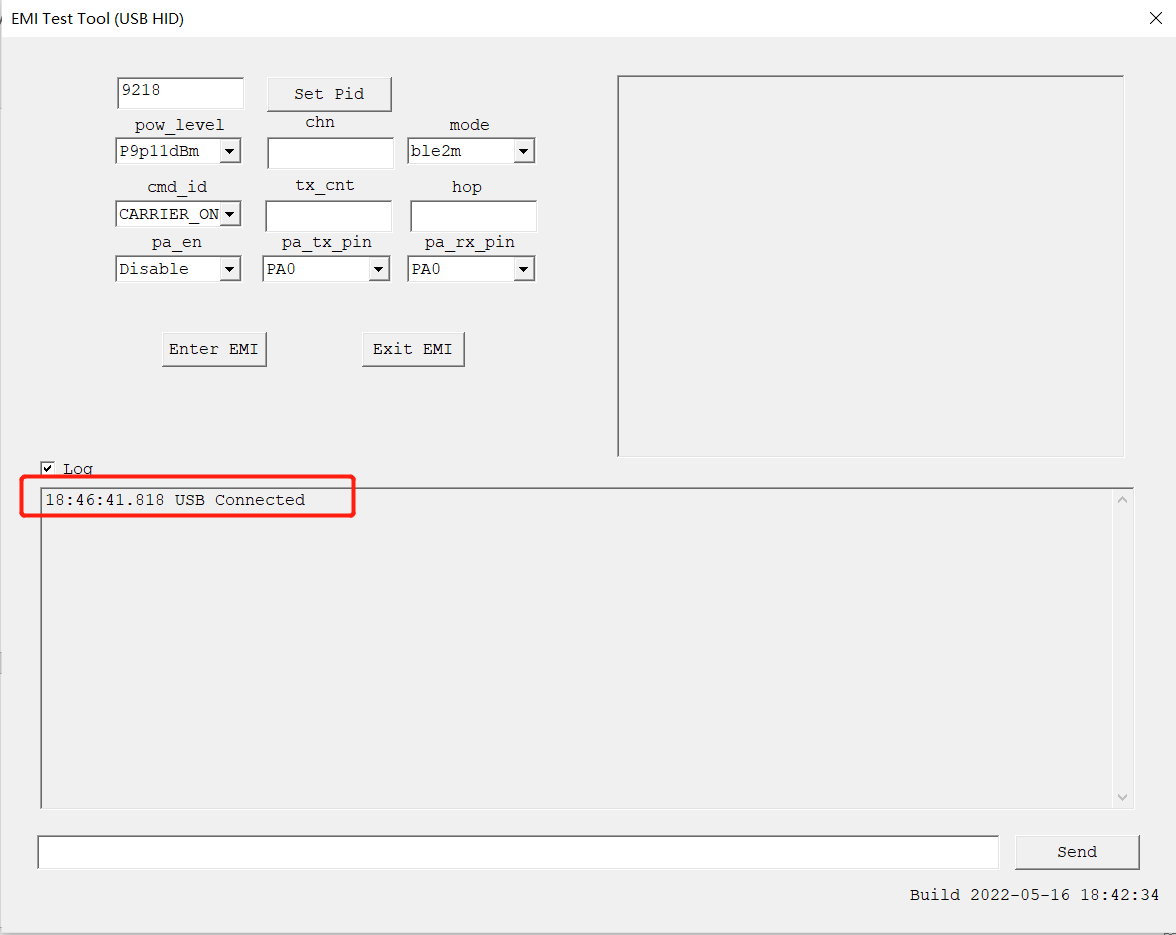
The default pid is 9218. If the pid of the device to be tested has changed, enter the corresponding pid in the pid box and click "Set Pid".
Step 2: Configure the EMI parameters, click "Enter EMI", as shown in the figure, the EMI test will be printed in the RISC-V TDB tool, and print the corresponding configuration parameters.
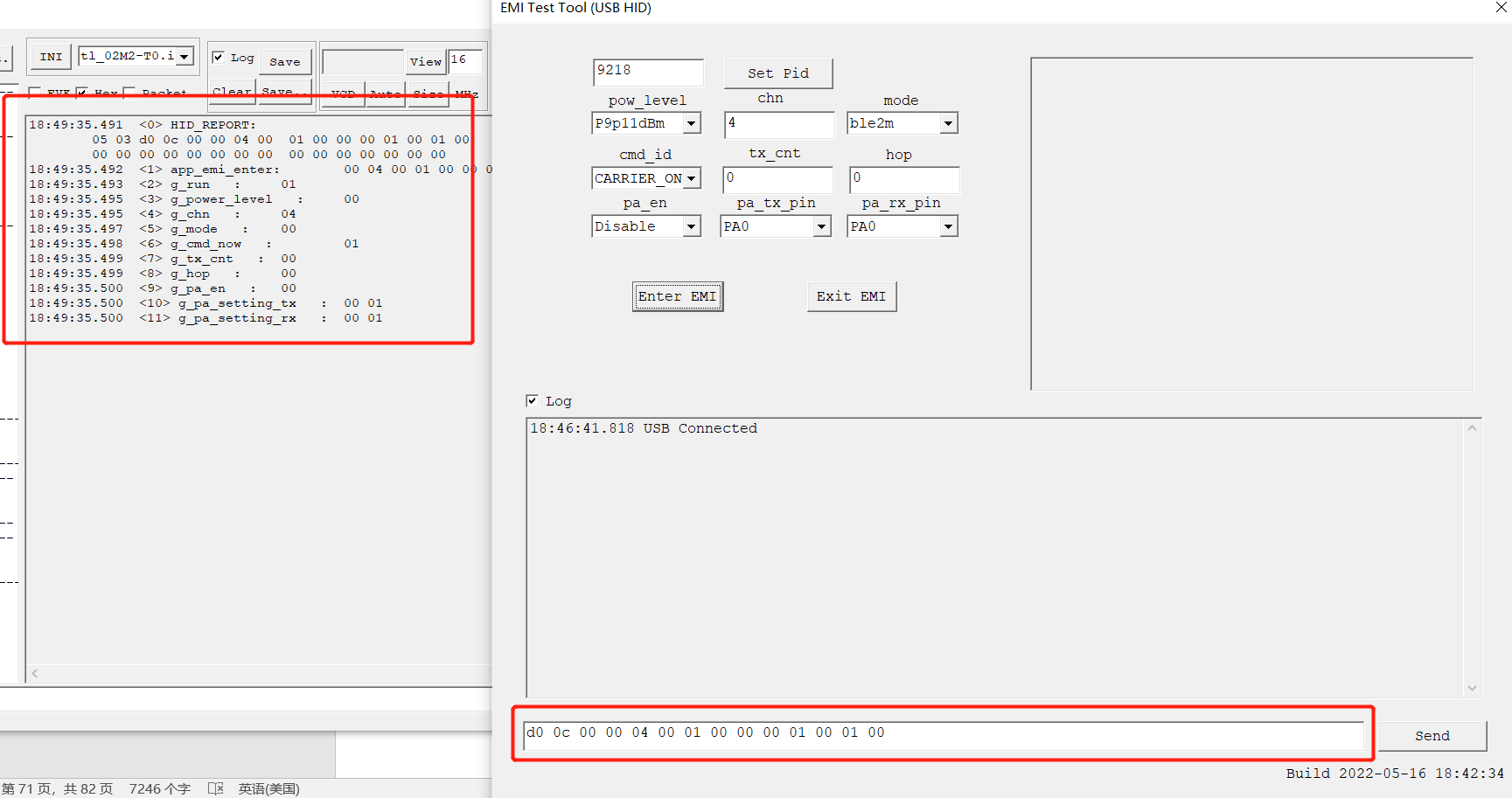
Step 3: Click "Exit EMI" to exit EMI mode (Note: to modify the configuration, you need to click Exit EMI to exit EMI mode first, and then click Enter EMI to re-enter EMI, thus enabling the configuration modification).

The microphone SDK is generally divided into a transmitter side and a receiver side according to its function, referred to below as TX and RX. Usually TX is the signal sampling end, the signal is captured and then compressed/encoded and the data is sent via a wireless 2.4GHz signal. Taking the ultra-low latency SDK as an example, the corresponding projects are _proj_ultra_ll_mic_tx and _proj_ultra_ll_mic_240_tx. RX is to receive the data sent from TX end through the 2.4GHz signal, decode/decompress the data and output audio through USB Audio or Line-out. Taking the ultra-low latency SDK as an example, the corresponding projects are _proj_ultra_ll_mic_rx and _proj_ultra_ll_mic_240_rx.
After importing the SDK project in the IDE, the displayed file structure is shown in the following figure. There are 10 top-level folders: algorithm, application, boot, common, drivers, incs, proj_lib, stack, vendor.
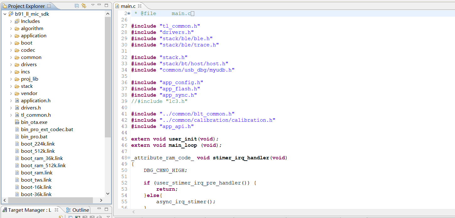
algorithm: Algorithm related programs, aes_ccm, crypto, ecc.
application: Provides some generic application handlers such as print, keyboard etc.
boot: Provides the software bootloader for the chip, i.e. the assembly process after the MCU is powered on or waked up by deepsleep, to set up the environment for the C program to run later.
codec: Codec related algorithms, such as filter, resample, etc.
common: Provides some general cross-platform handling functions, such as memory handling functions, string handling functions, etc.
drivers: Provides hardware settings and peripheral drivers that are closely related to the MCU, such as clock, flash, I2C, USB, GPIO, UART, etc.
incs: Public header file directory.
proj_lib: Stores the library files necessary for the SDK to run (e.g. libB91_driver_i2.a). The BLE stack, RF driver, PM driver and other files are encapsulated in the library files, and users cannot see the source files.
stack: Stores the header files related to the BLE/BT protocol stack. The source files are compiled into library files and are not visible to the user.
vendor: Stores user application layer code.
boot: Stores the cstartup_9518.S file. cstartup_9518.S: completes the initialization, move and copy of retention_reset, aes_data, retention_data, ramcode, data, sbss, bss, stack, flash initialization, interrupt vector entry, and some functions that need to be written in assembly.
bootlink: Flash, I-RAM, D-RAM layout file.
boot.link: The bootlink corresponding to the _proj_boot_xx project.
boot-36k.link: The bootlink corresponding to the project under vendor, the difference is that the SRAM and the corresponding flash address are offset by 0x9000 (36k).
It includes the main function entry, the related functions of system initialization, and the writing of the infinite loop while(1). It is recommended not to make any modifications to this file, and directly use inherent writing (some unimportant codes have been omitted).
_attribute_ram_code_ int main(void)
{
    blc_pm_select_internal_32k_crystal();
    sys_init(DCDC_1P4_LDO_1P8,VBAT_MAX_VALUE_GREATER_THAN_3V6);
    clock_init(PLL_CLK_192M, PAD_PLL_DIV, PLL_DIV2_TO_CCLK, CCLK_DIV2_TO_HCLK, HCLK_DIV2_TO_PCLK, PLL_DIV4_TO_MSPI_CLK);

user_read_flash_value_calib();

#if WATCHDOG_ENABLE
    wd_set_interval_ms(15*1000);
    wd_start();
#endif

user_init();

    while(1)
{

        main_loop();
#if WATCHDOG_ENABLE
        wd_clear_cnt();
#endif
    }
    return 0;
}(1) app_config.h
The application function configuration file is used to configure the application function parameters of the whole system, including the configuration of 2.4GHz related functions, USB related functions, audio input functions and algorithm related functions.
(2) app_audio_config.h
The audio function configuration file is used to configure the audio function parameters, including the configuration of the encoder, frame length, gain and other related functions.
(3) app_ui.h
The UI function configuration file is used to configure the UI function parameters, including the configuration of related functions such as key, led, power detection, and tone.
The meaning of each parameter in the configuration file is explained later in the introduction to each module.
The BootLoader projects including TX and RX, _proj_bootdongle and _proj_bootdevice respectively. After power-on, it will detect APP firmware integrity and jump to the APP for execution. In the APP firmware, you can also call the function to enter the BootLoader to perform the OTA operation. For the operation method of OTA, please refer to the OTA Tool section.

The Ultra Low Latency MIC supports 2-to-1/1-to-1 format, and has the characteristics of low latency and strong anti-interference, etc. The effective use distance is related to the product format and transmission times, and needs to be tested according to the actual product. Ty/uploads/zip/20230213112102661G2/pical 2-to-1 audio performance is as follows:
Analog input and output: latency as low as 8ms (SBC codec) and 12ms (LC3+ codec), frequency response 20 ~ 20kHz, THD+N as low as 0.5%, and SNR reaches 88dB.
IIS input and output: latency as low as 7ms (SBC codec) and 9ms (LC3+ codec), frequency response 20 ~ 20kHz, THD+N as low as 0.04%, and SNR reaches 96dB.
The SDK provides users with two project demos: _proj_ultra_llmic and _proj_ultra_ll_mic240, as shown below:
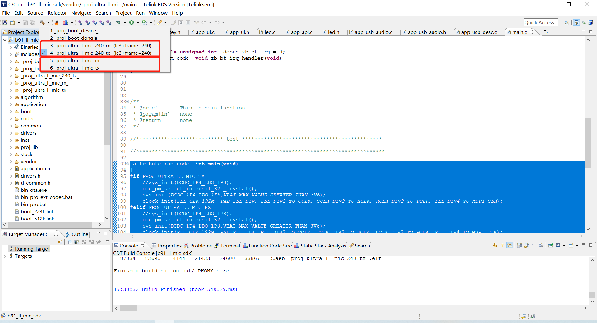
The _proj_ultra_llmic and _proj_ultra_ll_mic240 projects are in fact not fundamentally different, but simply differ in the encoding-related configuration used by default to facilitate a quick evaluation, as follows.
Project _proj_ultra_llmic _proj_ultra_ll_mic240
Default encoding LC3+ LC3+
Number of retransmission 4 (default) 7 (longer transmission distance)
Frame length 120 sampling points (default) 240 sampling points (Better sound quality)
Table: SDK demo encoding related configuration
The specific functions of the TX end are as follows.
(1) Supported application related functions:
a) USB module: USB HID, USB Debug;
b) Watchdog module;
c) Algorithm module: including EQ, noise reduction algorithm, resampling algorithm, DRC algorithm;
d) OTA module;
e) EMI module: support EMI test instructions;
f) 2.4GHz module: RF related: 2.4GHz Tx, transmit power adaptive, frequency hopping; wireless related: manual pairing, reconnection, and automatic pairing.
(2) Supported audio related functions:
a) Coding: SBC, LC3+;
b) Audio input: AMIC, DMIC, Line-in, I2S.
(3) Supported UI related functions:
a) KEY: short press, long press, double click;
b) LED;
c) TTONE: tones;
d) Power detection.
The UI function of the RX end is the same as that of the TX end, other functions are as follows.
(1) Supported application related functions:
a) USB module: USB Audio upstream and downstream, USB HID, USB Debug;
b) Watchdog module;
c) OTA module: OTA upgrade;
d) EMI module: supports EMI fixed frequency test;
e) 2.4GHz module: RF related: 2.4GHz Rx, frequency hopping, packet error correction; wireless related: manual pairing, reconnection, automatic pairing, one-to-one, one-to-two.
(2) Supported audio related functions:
a) Coding: SBC,LC3+;
b) Audio output: local Line-out, I2S, USB Audio.
Many functions of the SDK are controlled via macro switches. The following briefly introduces app_config.h, app_audio_config.h, and app_ui.h.
MIC_TX_NUM:
Default value: 2;
Function description: control the number of Tx;
Remark: the default 2-to-1 mode can be modified to 1-to-1 mode, the time slot becomes shorter and the number of TX retransmissions will increase accordingly.
AUTO_PAIR_EN:
Default value: 0;
Function description: automatic pairing.
TRANSMIT_DATA_EN:
Default value: 0;
Function description: transmit command;
Remark: Transmit bootloader command.
ADAPTIVE_RF_POWER_EN:
Default value: 0;
Function description: transmitting power adaptive adjustment function.
RF_ERROR_CORRECTION_EN:
Default value: 0;
Function description: packet error correction function.
APP_MODE:
Default value: APP_MODE_DEBUG_ONLY;
Function description: USB mode selection;
Remark: default PRINTER debug mode, can be adjusted to USB HID mode as well as USB Audio.
USB_SPEAKER_ENABLE:
Default value: 1;
Function description: USB Audio downstream enable;
Remark: it is enabled by default and can be disabled individually.
USB_MIC_ENABLE:
Default value: 1;
Function description: USB Audio upstream enable;
Remark: it is enabled by default and can be disabled individually.
WATCHDOG_ENABLE:
Default value: 1;
Function description: watchdog enable.
EMI_TEST_ENABLE:
Default value: 0;
Function description: EMI function enable.
APP_NS_ENABLE:
Default value: 0;
Function description: noise cancelling function enable.
APP_EQ_ENABLE:
Default value: 0;
Function description: EQ function enable.
ADC_DRC_EN:
Default value: 0;
Function description: DRC function enable.
LED_ENABLE:
Default value: 1;
Function description: LED enable;
Remark: LED_BLUE, LED_GREEN, LED_WHITE, LED_RED are defined respectively.
KEY_ENABLE:
Default value: 1;
Function description: KEY enable.
TTONE_EN:
Default value: 1;
Function description: tone enable;
Remark: to play the tone, the tone bin file needs to be burned.
ENABLE_BATT_CHECK:
Default value: 0;
Function description: power detection enable;
Remark: the PB3 pin is used by default and can be modified at the initialization of the bat_check_init interface.
CODEC_DAC_MONO_MODE:
Default value: 1;
Function description: 1: mono, 0: stereo;
Remark: the Lineout on the Tx end is used to monitor input audio, it is enabled by default and can be disabled.
CODEC_ALGORITHM_SEL:
Default value: CODEC_ALGORITHM_LC3A;
Function description: codec selection;
Remark: LC3+ encoding is selected by default, and SBC encoding can be selected.
LC3A_BIT_RATE:
Default value: 96000(72000);
Function description: LC3+ bit rate;
Remark: LC3+ uses 96k bit rate at 120 Samples (72k for proj_ultra_ll_mic_240 project).
MIC_SAMPLING_RATE:
Default value: 48000;
Function description: mic sample rate;
Remark: default 48k.
MIC_SAMPLES_PER_PACKET:
Default value: 120 (240 for proj_ultra_ll_mic_240 project);
Function description: mic sample;
Remark: the default sample is 2.5ms (5ms), so mic one sample = 2.5(5)*48000/1000= 120(240).
MIC_PACKET_NUM:
Default value: 8(14);
Function description: the number of times that Tx sends audio packets;
Remark: In the case of 1-to-2 (discussed separately for 1-to-1), the Tx end retransmits 8/2 = 4 times per packet of audio data, and the specific value is affected by the time slot and coding.
AUDIO_INTERFACE:
Default value: AUDIO_I2S_CODEC;
Function description: codec audio source selection;
Remark: the default is the internal codec input and output. If it is changed to AUDIO_I2S_GPIO, it will be switched to I2S input and output.
AUDIO_IN_MODE:
Default value: LINE_INPUT;
Function description: Internal codec input source selection;
Remark: when AUDIO_INTERFACE is configured as AUDIO_I2S_CODEC, internal codec input source selection can be performed with this macro, supporting AMIC, DMIC, Linein.
AUDIO_INTERFACE_ROLE:
Default value: AUDIO_I2S_AS_MASTER;
Function description: external pin input source master-slave selection;
Remark: when AUDIO_INTERFACE is configured as AUDIO_I2S_GPIO, the I2S role can be configured as master/slave through this macro.
MIC_AB_EN:
Default value: 0;
Function description: A mic and B mic functions enable.
MIX_ADC_AUDIO_EN:
Default value: 0;
Function description: Rx end mixed local mic function enable;
Remark: Rx end.
CODEC_IN_A_GAIN:
Default value: CODEC_IN_A_GAIN_0_DB;
Function description: AMIC input gain;
Remark: when the Tx end AUDIO_IN_MODE is configured as AMIC_INPUT, the AMIC input gain can be configured through this macro.
CODEC_IN_D_GAIN:
Default value: CODEC_IN_D_GAIN_0_DB;
Function description: DMIC input gain;
Remark: when the Tx end AUDIO_IN_MODE is configured as DMIC_INPUT, the DMIC input gain can be configured through this macro.
CODEC_OUT_A_GAIN:
Default value: CODEC_OUT_A_GAIN_0_DB;
Function description: analog output gain;
Remark: Used to configure analog output gain of Tx end and Rx end.
CODEC_OUT_D_GAIN:
Default value: CODEC_OUT_D_GAIN_0_DB;
Function description: digital output gain;
Remark: Used to configure digital output gain of Tx end and Rx end.
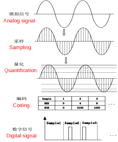
Sampling: Take a point at a certain time interval for the analog signal.
Quantification: Add a scale to the vertical coordinate, and take an integer value according to the approximation, so that the values of the obtained sampling points are all integers.
Coding: The integer value obtained by quantization is encoded in binary.
Digital signal: Turn the encoded sequence of 0 and 1 into high and low level signals.
Pulse code modulation, or PCM for short. It can be seen from the above analog-to-digital conversion that the content stored in the PCM format file is actually the sequence obtained by encoding.
Sampling frequency: Sampling is to digitize the analog signal on the time axis, According to the Nyquist theorem (sampling theorem), sampling is performed at a frequency that is more than 2 times the highest frequency of the sound (AD conversion). Sounds with frequencies between 20Hz and 20kHz can be recognized by the human ear, so the sampling frequency is generally around 40kHz, the commonly used music is 44.1kHz (44100 times/s sampling), 48kHz, etc. The sampling rate for telephones is 8kHz.
Sampling bits: The range of data that each sample point can represent. The number of sampling bits is usually 8 bits or 16 bits, the larger the number of sampling bits, the more delicate the change of the sound that can be recorded, and the larger the corresponding amount of data. 16 bits is the most common sampling accuracy.
Number of channels: The number of channels refers to the number of speakers that can support different sounds, the number of channels commonly used are mono, stereo (left channel and right channel).
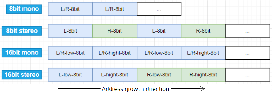
PCM is uncompressed audio data after sampling and quantization, which is standard digital audio data converted from analog signals through sampling, quantization, and encoding. If it is a mono audio file, the sampled data is stored in the order of time (if it 's a double channel, store it in LRLR mode), and the storage is also related to the big-endian/little-endian of the machine. The little-endian mode is shown below.
Supported codec: SBC, LC3Plus, ADPCM.
The SBC and LC3Plus are used for audio compression and decompression for air transmission, ADPCM decoding speed is fast, used to play the tone.
The Flash storage information takes the size of one sector (4K bytes) as the basic unit, because the erase of Flash is based on sector (the erase function is flash_erase_sector). In theory, the same type of information needs to be stored in one sector, and different types of information need to be stored in different sectors (to prevent other types of information from being erased by mistake when erasing information). Therefore, it is recommended that users follow the principle of "put different types of information in different sectors" when using Flash to store customized information.
The chip supports 1MB of Flash as the program storage space by default. The SDK defines "FLASH_SIZE" as 1MB at the end of the file boot.link, and makes a limit judgment on "BIN_SIZE" <= "FLASH_SIZE". If the user uses Flash larger than 1MB, the description needs to be modified accordingly.
Flash is divided into Locked area and Unlocked area according to function, which respectively store data that does not need to be changed and data that can be changed at any time. Data that will be changed, such as pairing information, is stored in the Unlocked area, while data that will not be changed, such as firmware, version information, USB_ID, tone, DRC parameters, and EQ parameters, are stored in the Locked area.
(1) The sector 0xFF000 ~ 0xFFFFF stores the MAC address, in fact the 6 bytes of MAC address are stored in 0xFF000 ~ 0xFF005, the high byte address is stored at 0xFF005 and the low byte address is stored at 0xFF000. For example, if the contents of Flash 0xFF000 ~ 0xFF005 are 0x11 0x22 0x33 0x44 0x55 0x66 in order, then the MAC address is 0x665544332211.
Telink's mass production jig system will burn the MAC address of the actual product to the address 0xFF000, which corresponds to the SDK. If the user needs to modify this address, please make sure that the address burned by the jig system is also modified accordingly. In the SDK, the user_init function will read the MAC address from the CFG_ADR_MAC_1M_FLASH address of the Flash, this macro can be modified in /vendor/common/blt_common.h.
#ifndef             CFG_ADR_MAC_1M_FLASH
#define             CFG_ADR_MAC_1M_FLASH              0xFF000
#endif
(2) The two sectors 0xEA000 and 0xEB000 are occupied by the 2.4GHz protocol stack and are used to store pairing information.
(3) 0x00000 ~ 0x3FFFF 256KB space is used as program space by default. 0x00000 ~ 0x3FFFF total 256KB is firmware storage space. 0x40000 ~ 0x7FFFF 256KB is the space for storing new firmware during OTA update, that is, the supported firmware space is theoretically 256KB. For some special reason, the 0x40000 ~ 0x7FFFF high address space can actually only be used for 254KB, and the last 4KB cannot be used.
Note:
In fact the last 4KB of all high address spaces cannot be used.
(4) 0xDF000 is the MAC address for the mass production, and we use this address as MAC address by default. If the address does not store data, the address where 0xFF000 is will be read.
(5) 0xDC000 is the EQ data storage address.
(6) 0xDA000 is the USB PID VID storage address.
(7) 0xD9000 is the DRC algorithm data storage address.
(8) 0x80000 is the tone storage address.
(9) 0x7FFF0 is the USB_ID storage address.
(10) The remaining Flash space is all used as the user's data storage space.
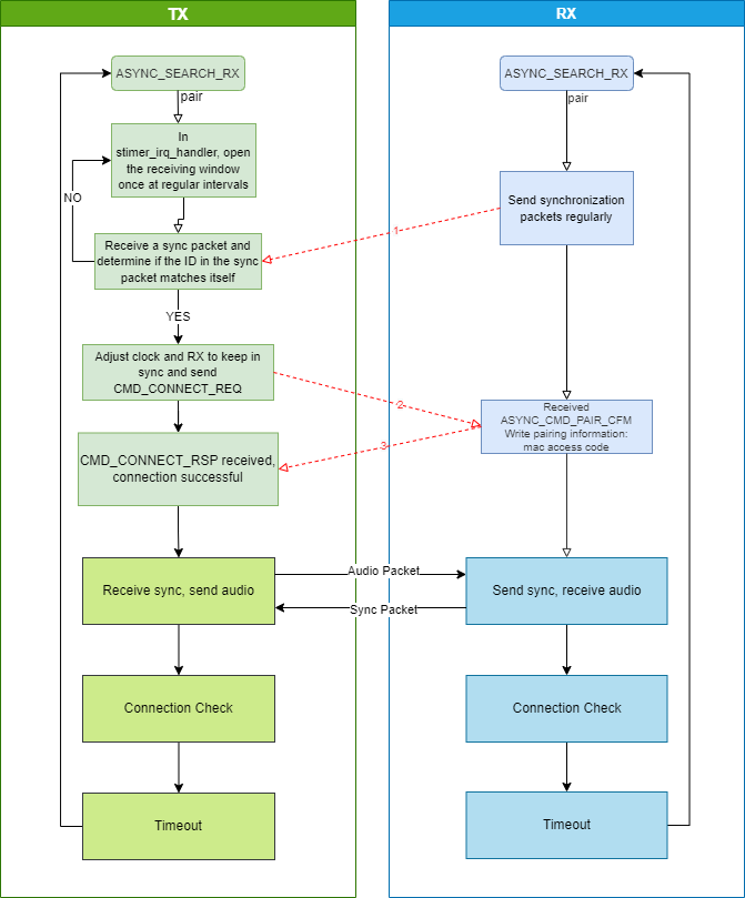
async_init: Initialize system timer, initialize RF, frequency hopping, timing parameters and various interrupts;
async_stx_start: RF packet sending function;
async_srx_start: RF packet receiving function;
async_irq_rf: RF interrupt handling function.
The MCU is in working mode during normal program execution, and the working current is between 3 ~ 7mA. If you need to save power, the chip needs to enter the low power mode.
Low power mode, also known as sleep mode, includes three types: suspend mode, deepsleep mode, and deepsleep retention mode.
The SDK currently supports deepsleep mode, at this time, the program stops running, most of the hardware modules of the MCU are powered down, while the PM hardware modules remain operational. In deepsleep mode the IC current is less than 1uA, if the standby current of the built-in flash is around 1uA, this may result in a measured deepsleep current of 1 ~ 2uA. When deepsleep mode wakes up, the MCU will restart, similar to the effect of power on, and the program will restart to initialize.
In Deepsleep mode, except for a few registers on the analog register that can save the state, all other SRAM, digital register, and analog register lose state when powered down.
The PM module special non-power-down analog regsiter, DEEP_ANA_REG in the drivers/B91/pm.h file, as shown in the following code.
#define PM_ANA_REG_POWER_ON_CLR_BUF0    0x39 // initial value 0x00. [Bit0][Bit1] is already occupied. The customer cannot change!
#define PM_ANA_REG_POWER_ON_CLR_BUF1    0x3a // initial value 0x00
#define PM_ANA_REG_POWER_ON_CLR_BUF2    0x3b // initial value 0x00
#define PM_ANA_REG_POWER_ON_CLR_BUF3    0x3c // initial value 0x00
#define PM_ANA_REG_POWER_ON_CLR_BUF4    0x3d // initial value 0x00
#define PM_ANA_REG_POWER_ON_CLR_BUF5    0x3e // initial value 0x00
#define PM_ANA_REG_POWER_ON_CLR_BUF6    0x3f // initial value 0x0f
#define PM_ANA_REG_POWER_ON_CLR_BUF7    0x38 //initial value =0xff
The registers above 0x3f will only restore the initial value when powered down. It should be noted that customers are not allowed to use ana_39, this analog register is reserved for use by the underlying stack, if the application layer code uses this register, it needs to be modified to ana_3a ~ ana_3f. Because the number of non-power-down analog registers is relatively small, it is recommended that customers use each bit to indicate different status bit information.
The 0x38 register will be initialized in the three cases: hardware/software reset, power down and watchdog. It should be noted that the bit0 bit is already used by stack, and users need to avoid this bit when using it.
The user can use the return value of the API pm_get_mcu_status(void) after sys_init(power_mode_e power_mode) to determine which state the cpu returns from, the return value is as follows:
typedef enum{
MCU_STATUS_POWER_ON = BIT(0),
MCU_STATUS_REBOOT_BACK = BIT(2), //the user will not see the reboot status.
MCU_STATUS_DEEPRET_BACK = BIT(3),
MCU_STATUS_DEEP_BACK = BIT(4),
MCU_STATUS_REBOOT_DEEP_BACK = BIT(5), //reboot + deep
}pm_mcu_status;The suspend/deepsleep/deepsleep retention can be woken up by GPIO PAD and timer. This SDK only focuses on 2 wake-up sources, as shown below (Note that the two definitions of PM_TIM_RECOVER_START and PM_TIM_RECOVER_END in the code are not wake-up sources).
typedef enum {
Telink B91 BLE Single Connection SDK Developer Handbook
AN-20111001-C2 217 Ver.0.2.0
PM_WAKEUP_PAD = BIT(3),
PM_WAKEUP_TIMER = BIT(5),
}SleepWakeupSrc_TypeDef;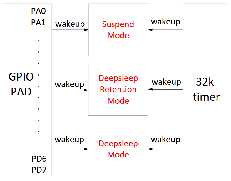
As shown in the figure above, deepsleep mode has 2 wake-up sources in hardware: timer and GPIO PAD.
The wake-up source PM_WAKEUP_TIMER comes from hardware 32k timer (32k RC timer or 32k Crystal timer). The 32k timer has been correctly initialized in the SDK, and the user does not need any configuration when using it, just set the wake-up source in cpu_sleep_wakeup().
The wake-up source PM_WAKEUP_PAD comes from the GPIO module, and the high and low levels of all GPIOs (PAx/PBx/PCx/PDx/PEx) except the 4 pins of MSPI have wake-up function.
The API for configuring GPIO PAD to wake up sleep mode:
typedef enum{
    WAKEUP_LEVEL_LOW        = 0,
    WAKEUP_LEVEL_HIGH       = 1,
}pm_gpio_wakeup_level_e;
void pm_set_gpio_wakeup (gpio_pin_e pin, pm_gpio_wakeup_Level_e pol, int en);
#define cpu_set_gpio_wakeup pm_set_gpio_wakeup
pin is defined for GPIO.
pol is the definition of wake-up polarity: Level_High means high level wake-up, Level_Low means low level wake-up.
en: 1 means enable, 0 means disable.
For example:
cpu_set_gpio_wakeup (GPIO_PC2, Level_High, 1); //GPIO_PC2 PAD wake-up on, high level wake-up
cpu_set_gpio_wakeup (GPIO_PC2, Level_High, 0); //GPIO_PC2 PAD wake-up off
cpu_set_gpio_wakeup (GPIO_PB5, Level_Low, 1);  //GPIO_PB5 PAD wake-up on, low level wake-up
cpu_set_gpio_wakeup (GPIO_PB5, Level_Low, 0);  //GPIO_PB5 PAD wake-up off
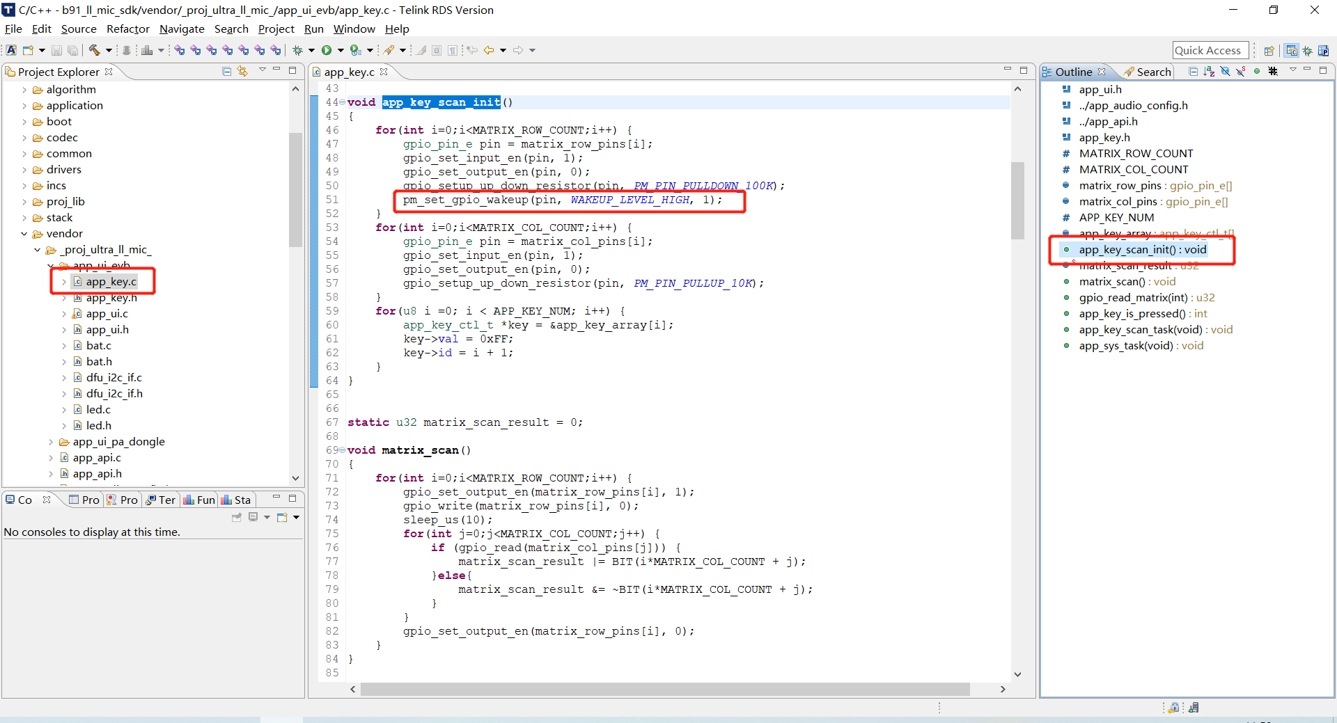
In the ui definition of EVB, all the corresponding pins of the buttons are configured as wake-up on, high level wake-up:
The API to set the MCU to go to sleep and wake up:
typedef int (*cpu_pm_handler_t)(SleepMode_TypeDef sleep_mode, SleepWakeupSrc_TypeDef wakeup_src, unsigned int
wakeup_tick);
cpu_pm_handler_t cpu_sleep_wakeup;
The first parameter sleep_mode: used to set the sleep mode, there are the following 4 options, namely suspend mode, deepsleep mode, deepsleep retention 32K Sram, deepsleep retention 64K Sram.
typedef enum {
//available mode for customer
SUSPEND_MODE = 0x00,
DEEPSLEEP_MODE = 0x30,
DEEPSLEEP_MODE_RET_SRAM_LOW32K = 0x21, //for boot from sram
DEEPSLEEP_MODE_RET_SRAM_LOW64K = 0x03, //for boot from sram
DEEPSLEEP_MODE_RET_SRAM = 0x21,
//not available mode
DEEPSLEEP_RETENTION_FLAG = 0x0F,
}SleepMode_TypeDef;
The second parameter wakeup_src: set the wakeup source for the current suspend/deepsleep, and the parameter can only be one or more of PM_WAKEUP_PAD and PM_WAKEUP_TIMER. If wakeup_src is 0, then it cannot be woken up after entering low power sleep mode.
The third parameter wakeup_tick: when PM_WAKEUP_TIMER is set in wakeup_src, wakeup_tick needs to be set to determine when the timer wakes up the MCU, if PM_WAKEUP_TIMER is not set to wake up, this parameter is meaningless. The value of wakeup_tick is an absolute value, which is set according to the System Timer tick introduced earlier in this document, when the value of the System Timer tick reaches the set wakeup_tick, sleep mode is woken up. The value of wakeup_tick needs to be based on the value of the current System Timer tick and the absolute time converted from the time to sleep to effectively control the sleep time. If the wakeup_tick is set directly without considering the current System Timer tick, the wakeup time cannot be controlled. Since wakeup_tick is an absolute time, it must be within the range that the 32bit System Timer tick can represent, so the maximum sleep time that this API can represent is limited. The current design is that the maximum sleep time is 7/8 of the corresponding time of the maximum System Timer tick represented by 32 bits. The maximum System Timer tick can represent about 268s, then the longest sleep time is 268 * 7/8 = 234s, that is, the following delta_Tick cannot exceed 234s. If a longer sleep time is required, the user can call the long sleep function.
cpu_sleep_wakeup(SUSPEND_MODE, PM_WAKEUP_TIMER, clock_time() + delta_tick);The return value is the set of wake-up sources for the current sleep mode, and the wake-up sources corresponding to each bit of the return value are:
typedef enum {
WAKEUP_STATUS_COMPARATOR = BIT(0),
WAKEUP_STATUS_TIMER = BIT(1),
WAKEUP_STATUS_CORE = BIT(2),
WAKEUP_STATUS_PAD = BIT(3),
WAKEUP_STATUS_MDEC = BIT(4),
STATUS_GPIO_ERR_NO_ENTER_PM = BIT(7),
STATUS_ENTER_SUSPEND = BIT(30),
}pm_wakeup_status_e;
a) The bit of WAKEUP_STATUS_TIMER is 1, indicating that the current sleep mode is awakened by Timer.
b) The bit of WAKEUP_STATUS_PAD is 1, indicating that the current sleep mode is awakened by GPIO PAD.
c) When WAKEUP_STATUS_TIMER and WAKEUP_STATUS_PAD are 1 at the same time, it means that the two wake-up sources of Timer and GPIO PAD are in effect at the same time.
d) STATUS_GPIO_ERR_NO_ENTER_PM is a special state indicating that a GPIO wake-up error has currently occurred: For example, when a GPIO PAD is set to wake up at a high level, try to call cpu_sleep_wakeup to enter suspend when the GPIO is at a high level, and set the PM_WAKEUP_PAD wake-up source. At this time, it will fail to enter suspend, the MCU immediately exits the cpu_sleep_wakeup function, and returns value STATUS_GPIO_ERR_NO_ENTER_PM.
Use the following forms to control sleep time:
cpu_sleep_wakeup (SUSPEND_MODE , PM_WAKEUP_TIMER, clock_time() + delta_Tick);The delta_Tick is a relative time (such as 100* CLOCK_16M_SYS_TIMER_CLK_1MS), plus the current clock_time() it becomes an absolute time.
Example of cpu_sleep_wakeup usage:
cpu_sleep_wakeup (SUSPEND_MODE , PM_WAKEUP_PAD, 0);When the program executes this function, it enters suspend mode and can only be woken up by GPIO PAD.
cpu_sleep_wakeup (SUSPEND_MODE , PM_WAKEUP_TIMER, clock_time() + 10* CLOCK_16M_SYS_TIMER_CLK_1MS;When the program executes this function, it enters suspend mode and can only be woken up by Timer. The wake-up time is the current time plus 10ms, so the suspend time is 10ms.
cpu_sleep_wakeup (SUSPEND_MODE , PM_WAKEUP_PAD | PM_WAKEUP_TIMER,clock_time() + 50* CLOCK_16M_SYS_TIMER_CLK_1MS);When the program executes this function, it enters suspend mode and can be woken up by GPIO PAD and Timer. The wake-up time of Timer is set to 50ms. If the GPIO wake-up operation is triggered before the end of 50ms, the MCU will be woken up by the GPIO PAD; if there is no GPIO operation within 50ms, the MCU will be woken up by the Timer.
cpu_sleep_wakeup (DEEPSLEEP_MODE, PM_WAKEUP_PAD, 0);When the program executes this function, it enters deepsleep mode and can be woken up by GPIO PAD.
cpu_sleep_wakeup (DEEPSLEEP_MODE_RET_SRAM_LOW32K , PM_WAKEUP_TIMER, clock_time() + 8*
CLOCK_16M_SYS_TIMER_CLK_1S);
When the program executes this function, it enters deepsleep retention 32K Sram mode and can be woken up by the Timer, and the wake-up time is 8s after the function is executed.
cpu_sleep_wakeup (DEEPSLEEP_MODE_RET_SRAM_LOW32K , PM_WAKEUP_PAD | PM_WAKEUP_TIMER,clock_time() + 10*
CLOCK_16M_SYS_TIMER_CLK_1S);
When the program executes this function, it enters deepsleep retention 32K Sram mode, which can be woken up by GPIO PAD and Timer, and the timer wakeup time is 10s after the function is executed. If the GPIO wake-up operation is triggered before the end of 10s, the MCU will be woken up by the GPIO PAD; if there is no GPIO operation within 10s, the MCU will be woken up by the Timer.
When the user calls the API cpu_sleep_wakeup, the MCU enters the sleep mode; when the wake-up source triggers the MCU to wake up, the software running process of the MCU is inconsistent for different sleep modes.
The following details the MCU running flow after deepsleep is woken up. Please refer to the diagram below.
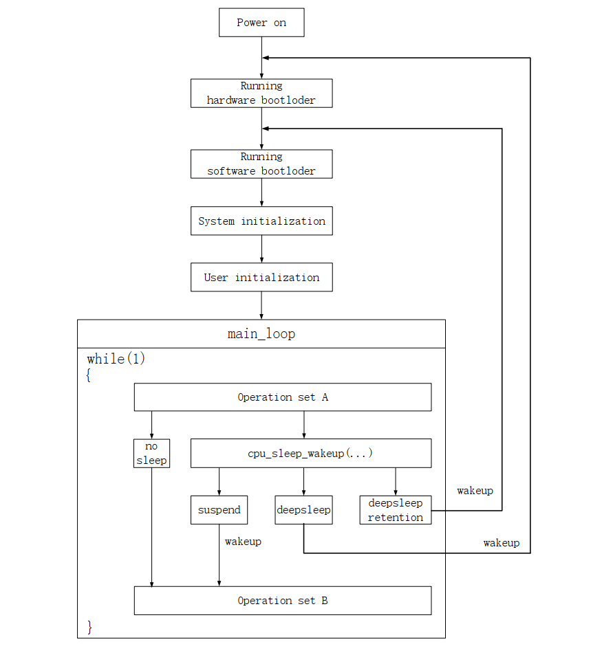
After the MCU is powered on, the introduction of each process:
(1) Run hardware bootloader
The MCU hardware performs some fixed operations, which are solidified on the hardware and cannot be modified by software.
A few examples to illustrate these operations, such as: chip power-on/deep wake-up: by reading the Flash boot and marking "TLNK", determine the current firmware storage address that should be running (offset address 0x00000/0x20000/0x40000/0x80000), then jump to the corresponding address of Flash (base address 0x20000000 + offset address 0x00000/0x20000/0x40000/0x80000) to start executing the software bootloader.
(2) Run software bootloader
After the hardware bootloader finishes running, the MCU starts to run the software bootloader. Software bootloader is the vector end introduced earlier (corresponding to the assembler program in cstartup_B91.S).
Software bootloader is to set the memory environment for the running of the C language program, which can be understood as the initialization of the entire memory.
(3) System initialization
System initialization corresponds to the initialization of each hardware module (including sys_init, rf_drv_init, gpio_init, clock_init) between sys_init and user_init in the main function, which is used to set the digital/analog register status of each hardware module.
(4) User initialization
User initialization corresponds to the function user_init in the SDK.
(5) main_loop
After the user initialization is complete, it enters the main_loop controlled by while(1). A series of operations before entering sleep mode in main_loop is called "Operation Set A", and a series of operations after sleep wakeup is called "Operation Set B".
If the cpu_sleep_wakeup function is called to enter deepsleep mode, when deepsleep is woken up, the MCU will return to Run hardware bootloader again.
The process of deepsleep wake_up is almost the same as that of Power on, and all the hardware and software initialisation has to be done again.
After the MCU enters deepsleep, all Sram and digital/analog registers (except a few analog registers) will be powered down, so the power consumption is very low, and the MCU current is less than 1uA.
This document is uniformly described under the name "low battery detection".
For battery powered products, since the battery power will gradually decrease, when the voltage drops to a certain value, it will cause many problems:
(1) The working voltage range of B91 chip is 1.8V ~ 4.3v. When the voltage is lower than 1.8V, stable operation cannot be guaranteed.
(2) When the battery voltage is low, due to the instability of the power supply, the "write" and "erase" operations of the Flash may have the risk of errors, resulting in program firmware and user data being abnormally modified, which eventually leads to product failure. Based on previous mass production experience, we set the low voltage threshold that may present risks as 2.0V.
According to the above description, a secure voltage must be set for battery-powered products, only when the voltage is higher than this secure voltage can the MCU continue to work; once the voltage is lower than the secure voltage, the MCU stops running and needs to be shut down immediately (use to enter deepsleep mode in the SDK to achieve).
The secure voltage is also known as the alarm voltage, and this voltage value is currently used by default in the SDK at 2.2V. If the user has an unreasonable design in the hardware circuit that causes the stability of the power supply network to deteriorate, the secure voltage value will need to continue to be increased, e.g. 2.3V, 2.4V, etc.
For the developed product, as long as the battery is used for power supply, the low battery detection must be a task that runs in real time throughout the life cycle of the product to ensure product stability.
Low battery detection requires the use of an ADC to measure the supply voltage. User please refer to the ADC section of the "Driver SDK Developer Handbook" to gain the necessary understanding of the ADC module.
The implementation of low battery detection is described in combination with the implementation given by the SDK demo "proj_ultra_ll_mic_tx", refer to the files bat.c and bat.h.
It must be ensured that the macro "ENABLE_BATT_CHECK" in the app_config.h file is enabled, this macro is disabled by default, users need to pay attention when using the low battery detection function.
#define ENABLE_BATT_CHECK 1Low battery detection is a basic ADC sampling task. When implementing ADC to sample the power supply voltage, there are some issues that need to be paid attention to, which are explained as follows.
There are two sampling methods, which can be sampled by Vbat or GPIO analog signal input, but the Vbat channel sampling accuracy is poor, it is recommended to sample through external GPIO method in occasions that require high sampling accuracy.
The available GPIO input channels are the input channels corresponding to PB0~PB7, PD0, and PD1.
typedef enum{
    ADC_GPIO_PB0 = GPIO_PB0 | (0x1<<12),
    ADC_GPIO_PB1 = GPIO_PB1 | (0x2<<12),
    ADC_GPIO_PB2 = GPIO_PB2 | (0x3<<12),
    ADC_GPIO_PB3 = GPIO_PB3 | (0x4<<12),
    ADC_GPIO_PB4 = GPIO_PB4 | (0x5<<12),
    ADC_GPIO_PB5 = GPIO_PB5 | (0x6<<12),
    ADC_GPIO_PB6 = GPIO_PB6 | (0x7<<12),
    ADC_GPIO_PB7 = GPIO_PB7 | (0x8<<12),
    ADC_GPIO_PD0 = GPIO_PD0 | (0x9<<12),
    ADC_GPIO_PD1 = GPIO_PD1 | (0xa<<12),
}adc_input_pin_def_e;
The GPIO input channel is used for ADC sampling of the power supply voltage, the specific usage is as follows: in the hardware circuit design, the power supply is directly connected to the GPIO input channel. When the ADC is initialized, set GPIO to high impedance state (ie, oe, and output are all set to 0). At this time, the voltage of the GPIO is equal to the power supply voltage, and the ADC sampling can be performed directly.
During initialization, all states (ie, oe, output) can use the default state without special modification, PB3 is selected as the GPIO input channel by default in the demo.
Although the ADC input mode supports both single ended mode and differential mode, for some specific reasons, Telink stipulates that only differential mode can be used, and single ended mode is not allowed.
The input channel of differential mode is divided into positive input channel and negative input channel, and the measured voltage value is the voltage difference obtained by subtracting the negative input channel voltage from the positive input channel voltage.
If the ADC samples only one input channel, when using differential mode, set the current input channel as the positive input channel and GND as the negative input channel, so that the voltage difference between the two is equal to the voltage of the positive input channel.
Differential mode is used for low voltage detection in the SDK, and the function interface is as follows:
adc_set_diff_input(pin >> 12, GND);Low voltage detection as a most basic ADC sampling uses the Misc channel. In addition to low voltage detection, users will also need to use the Misc channel if they require other ADC tasks. Low voltage detection cannot run simultaneously with other ADC tasks and must be implemented by switching.
In the SDK demo, the proj_ultra_ll_mic and proj_ultra_ll_mic_240 projects both implement the low battery detection function, the user needs to enable the low battery detection function in app_ui.h for use.
The default initialization in the SDK is:
bat_check_init(ADC_GPIO_PB3, 0, 1, 2200, 2300);The first parameter pin: set the pin for low battery detection, SDK default PB3.
The second parameter res_up and the third parameter res_down: the voltage division coefficient of battery detection, because the low battery detection is based on GPIO, when the detection value exceeds 3.5V, the value will start to deviate. Therefore, when the detection voltage exceeds 3.5V, the user needs to configure the voltage division coefficient by himself, SDK default no voltage dividing, that is, the res_up value is 0, and the res_down value is 1. For the specific calculation position, refer to the following figure:
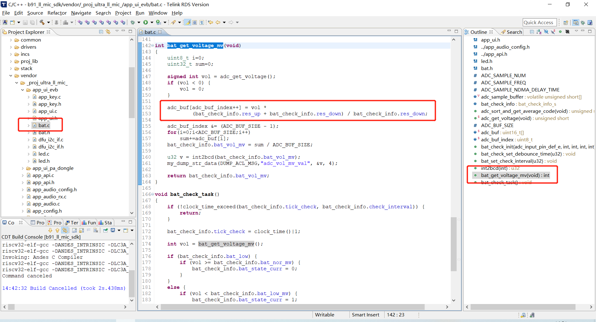
The fourth parameter bat_low_mv: secure voltage, SDK default 2200mV.
The fifth parameter bat_nor_mv: normal voltage, SDK default 2300mV, where the transition phase is between bat_low_mv and bat_nor_mv to prevent frequent switching between low power and normal state.
In addition, the bat_check_info variable is a low battery detection structure.
typedef struct {
    adc_input_pin_def_e pin;
    int res_up;
    int res_down;
    int bat_low_mv;
    int bat_nor_mv;

    u32 tick_debounce;
    u32 debounce_time;

    u32 tick_check;
    u32 check_interval;

    int bat_state_curr;
    int bat_state_last;

    int bat_low;
    int bat_vol_mv;
} bat_check_info_s;
The first five variables are input parameters for low battery detection initialization.
The sixth variable tick_debounce: low battery state switching timer, the default value is 1000 in microseconds, which is used to periodically switch the low battery state.
The seventh variable debounce_time: low battery state switching timing value, the default is 1000, unit microsecond.
The eighth variable tick_check: bat_check_task task execution timer, which is used to periodically execute the low battery detection task.
The ninth variable check_interval: bat_check_task task execution timing value, the default is 1000, unit microsecond.
The tenth variable bat_state_curr: the current low battery state.
The eleventh variable bat_state_last: the last low battery state. Judging with the current low battery state, if the current low battery state is inconsistent with the last low battery state, the update operation of the low battery state variable is started.
The twelfth variable bat_low: low battery state variable, 0 is non low battery state, 1 is low battery state, and the user can determine whether it is a low battery state by obtaining the variable state.
The thirteenth variable bat_vol_mv: current battery, unit mV.
In ui_loop, call bat_check_task() to realize low battery detection processing.
The frequency of the low battery detection task is controlled by the variable tick_check. In the Demo, the low battery detection is performed every 20ms, developers can modify this time value according to their own needs. When the working voltage changes from higher than 2300mV to lower than 2200mV, the bat_state_last value is 0 and bat_state_curr becomes 1. The current battery is inconsistent with the last battery, the low battery state variable update is started, and the value 1 of bat_state_curr is assigned to bat_low, thereby realizing the switching of the low battery state.
APP_MODE: to set the USB function, the following three settings are supported:
(1) APP_MODE_DEBUG_ONLY: support USB Log, VCD, command input;
(2) APP_MODE_DEBUG_HID: support USB Log, VCD, command input, HID communication;
(3) APP_MODE_AUDIO_AUTO: support USB Speaker, USB MIC, HID communication.
When APP_MODE == APP_MODE_AUDIO_AUTO, enable the USB Audio function, the following macros can be set:
a) USB_SPEAKER_ENABLE enable USB Speaker (USB downstream);
b) USB_MIC_ENABLE enable USB MIC (USB upstream);
c) USB_MIC_CHANNEL: 1: USB MIC/upstream Mono; 2: USB MIC/upstream Stereo.
Among them, USB Speaker and USB MIC can be enabled independently or simultaneously; USB Speaker only supports stereo.
The USB Audio descriptor name initialization is configured in the app_config.h file:
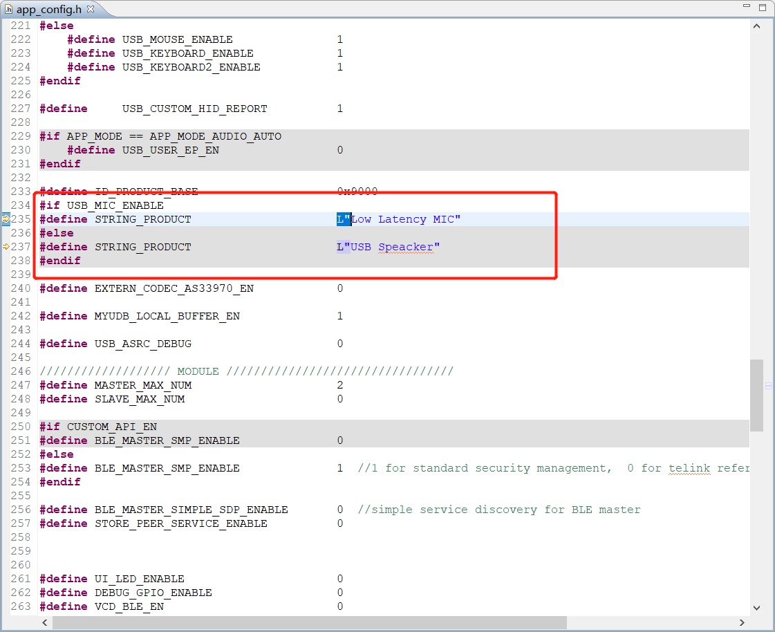
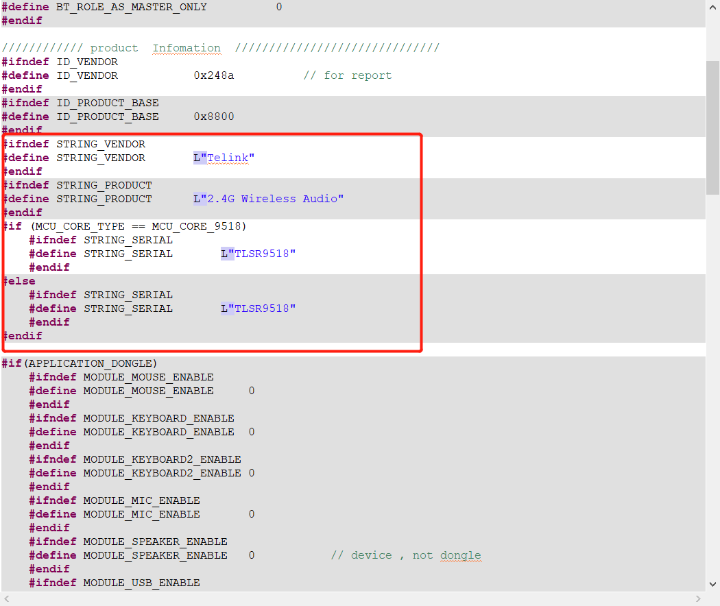
The default value is in the default_config.h file (as shown below), and it is recommended to modify it in app_config.h.
Calling the "my_resample48to16_init" and "my_resample16to48_init" interfaces correspond to the initialization of downsampling (48k-16k) and upsampling (16k-48k) respectively.
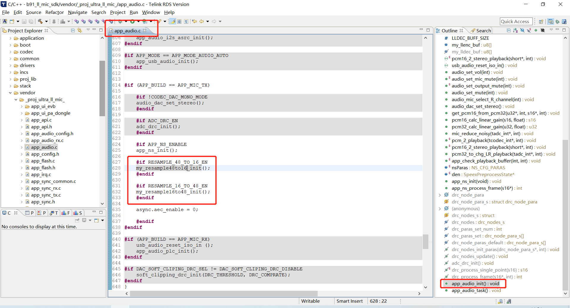
The current resampling algorithm processing is mainly suitable for the sampling rate adjustment problem in the noise canceling algorithm processing projects.
Before and after the noise canceling algorithm processing, the resampling algorithm is called for downsampling and upsampling. The specific reasons will be mentioned later.
Enable the APP_EQ_ENABLE macro to enable EQ.
#if(APP_BUILD == APP_MIC_TX) && APP_EQ_ENABLE
    eq_inf_load(0x20000000 + FLASH_USER_EQ_BASE);
    myudb_register_hci_eq_cb(my_debug_eq);
    audio_codec_flag_set(CODEC_FLAG_EQ_VOICE_MIC_EN, 1);
#endif
eq_inf_load(0x20000000 + FLASH_USER_EQ_BASE): used to read eq data, if the address does not store eq data, use the default eq parameters, as shown in the following figure:
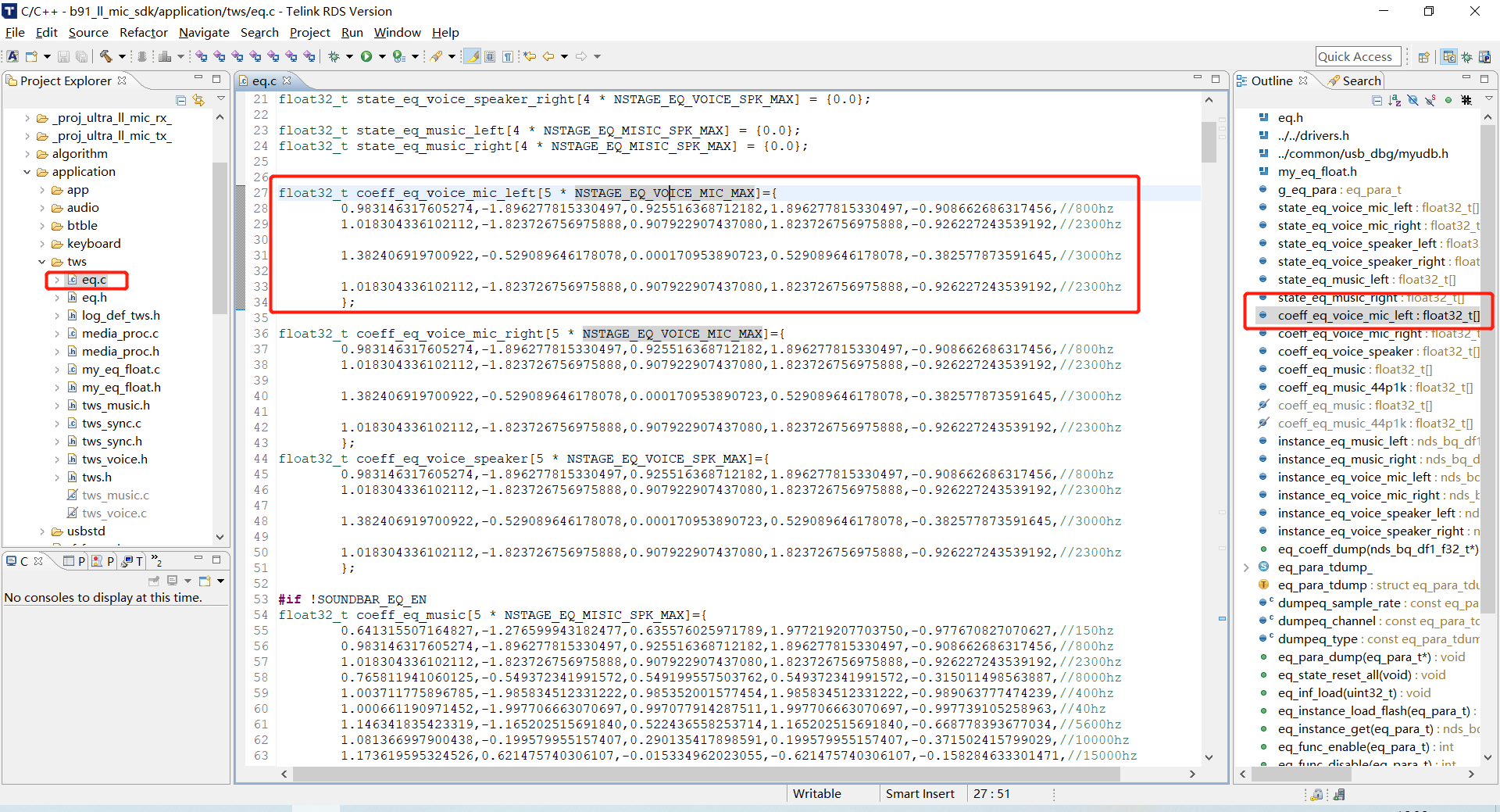
myudb_register_hci_eq_cb(my_debug_eq): used to register the EQ online debugging interface.
audio_codec_flag_set(CODEC_FLAG_EQ_VOICE_MIC_EN, 1): used to enable the EQ of the codec.
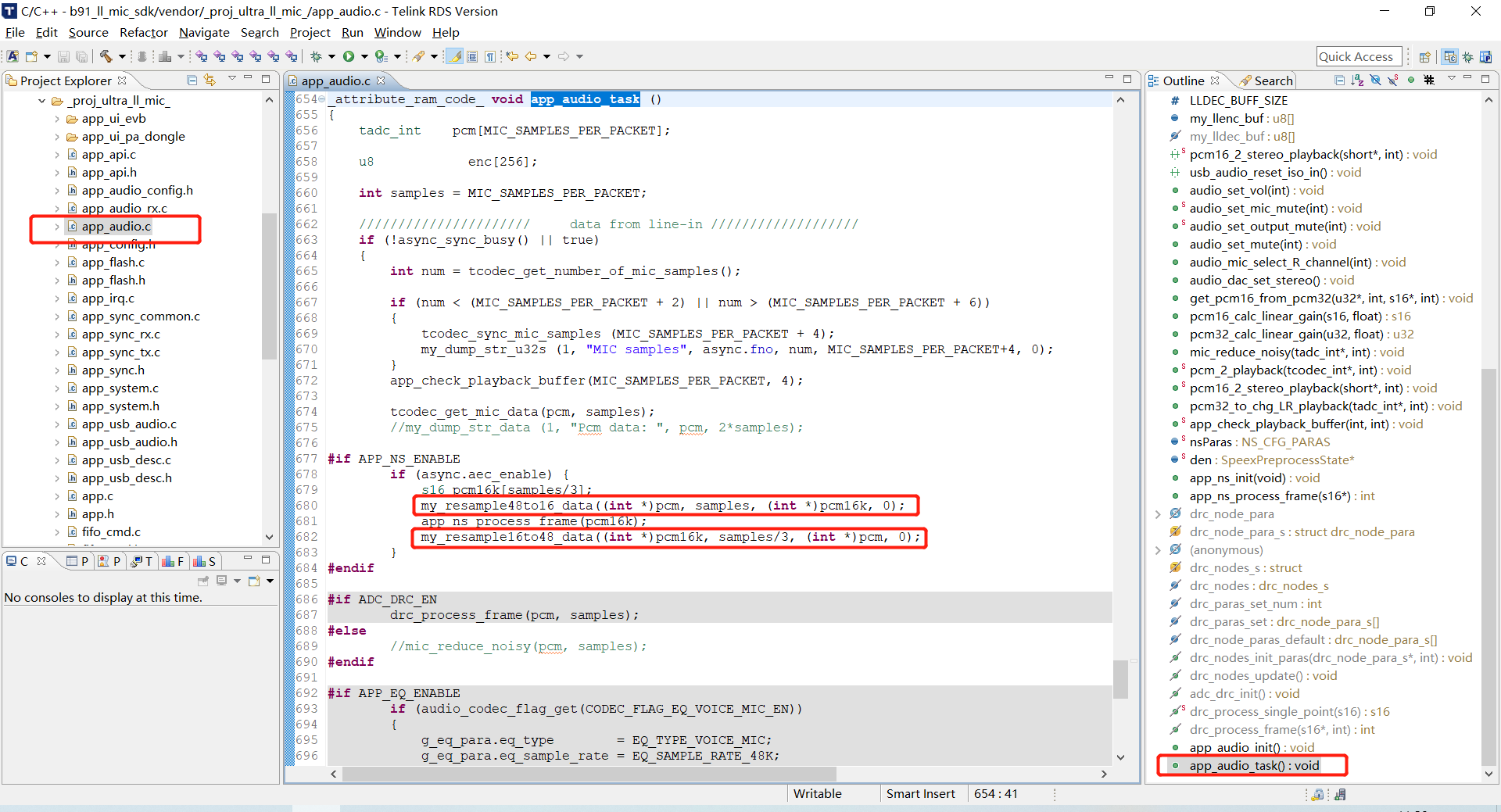
Performing EQ processing in the app_audio_task interface:
#if APP_EQ_ENABLE
        if (audio_codec_flag_get(CODEC_FLAG_EQ_VOICE_MIC_EN))
        {
            g_eq_para.eq_type        = EQ_TYPE_VOICE_MIC;
            g_eq_para.eq_sample_rate = EQ_SAMPLE_RATE_48K;

            g_eq_para.eq_channel = EQ_CHANNEL_LEFT;
            g_eq_para.eq_nstage = instance_eq_voice_mic_left.nstage;
            eq_proc(g_eq_para, pcm, pcm, samples, 0);
        }
#endif
EQ processing is performed by executing the eq_proc function.
EQ Tool is a tool used by Telink to debug EQ, the following introduces the EQ tool:
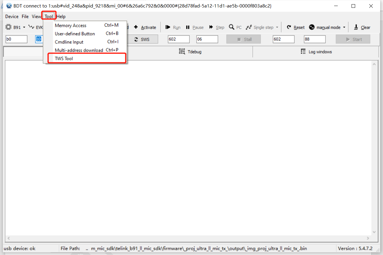
First open the Telink BDT tool, click "Tool", and in the drop-down menu, select "TWS Tool".
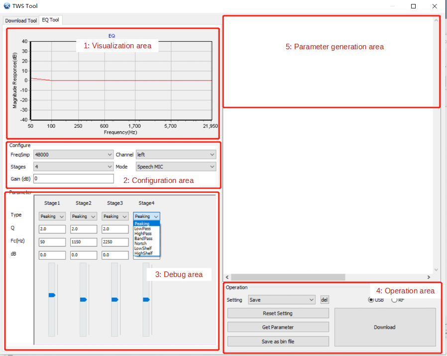
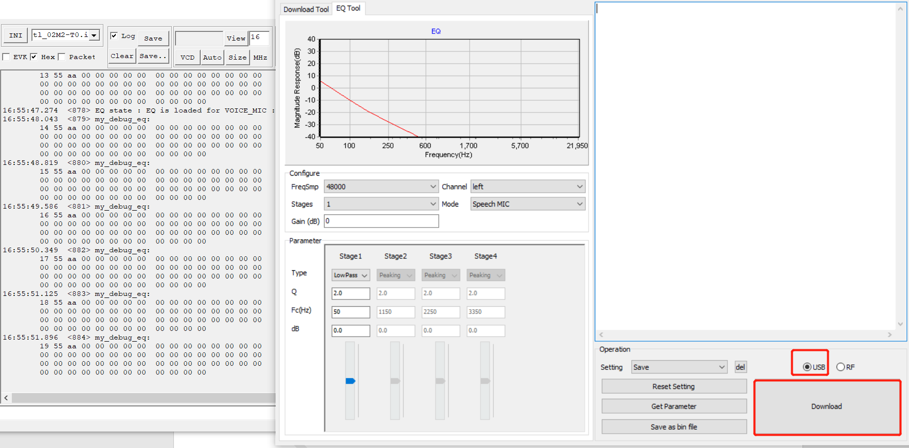
Select the "EQ Tool", which is divided into 5 main areas, namely:
(1) Visualization area: used to visualize EQ parameters for easy debugging.
(2) Configuration area: used to configure EQ initialization. Among them,
a) FreqSmp: sampling rate, SDK uses 48k by default;
b) Channel: supports left, right and stereo, the SDK uses the left channel by default;
c) Stages: the number of frequency points, 4 frequency points are supported by default;
d) Mode: EQ mode, SDK uses Speech Mic by default;
e) Gain: decrease the gain of all frequency points, the range is -10 ~ 0.
(3) Debug area: used to debug EQ parameters, among them,
a) Type: filter type;
b) Q: slope;
c) Fc(Hz): frequency point;
d) dB: gain.
(4) Operation area: used to update EQ parameters online, save EQ parameter bin files, and generate EQ parameter codes.
(5) Parameter generation area: used to display log and generate EQ parameters.
Next, show how to update the EQ parameters:
(1) USB online update: The APP_MODE macro is configured as APP_MODE_DEBUG_ONLY or APP_MODE_DEBUG_HID, to ensure that the device and PC can print the log, select "USB" in the operation area, click "Download", you can see the parameter update log in the risc-v TDB tool.
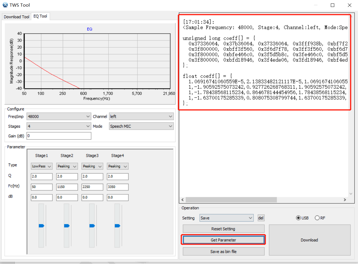
(2) Generate parameter update: Click "Get Paramter", the corresponding EQ parameter code will be generated in the generation parameter area, and replace the default eq parameter code mentioned above with this code.
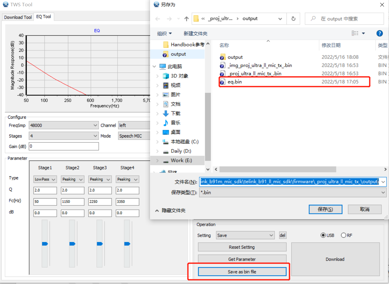
(3) Generate file update: Click "Save as bin file", generate the bin file of eq in the specified path, and then use the Download Tool of Telink TDB to burn the bin file to the address of 0xDC000.
Enable the APP_NS_ENABLE macro to enable the noise canceling algorithm.
Call the "app_ns_init" interface to initialize:
void app_ns_init(void)
{
    nsParas.noise_suppress_default = -15;
    nsParas.echo_suppress_default = -55;
    nsParas.echo_suppress_active_default = -45;
    nsParas.low_shelf_enable = 1;
    nsParas.ns_smoothness = 27853;      // QCONST16(0.85f,15)
    nsParas.ns_threshold_low = 0.0f;

#if 0
    int nsSize = ns_get_size();
    my_dump_str_data(1, "NS Buffer Size", &nsSize, 4);   // 0x234E
    den = (SpeexPreprocessState*)malloc(nsSize);
#else
    static u32 ns_buffer[0x234E/4+256];
    den = (SpeexPreprocessState*)ns_buffer;
#endif
    ns_init(den, &nsParas, MIC_SAMPLES_PER_PACKET/(MIC_SAMPLING_RATE/16000), SPEEX_SAMPLERATE);
}
noise_suppress_default: adjust the noise attenuation amplitude, the unit is db, -15 means attenuation 15db.
low_shelf_enable: the filter for low frequency attenuation. After enabling, there will be obvious attenuation below 100Hz, and the overall signal energy will also be reduced.
Note:
It is recommended not to modify other parameters.
Among them, the input parameter frame_size of the ns_init interface supports a maximum of 120.
The default mic sampling rate of the SDK is 48k, and the current version of the noise canceling algorithm is 16k. Therefore, before noise canceling processing, the audio data needs to be downsampled to 16k, and then upsampled back to 48k after noise canceling processing.

Dynamic Range Control (DRC) provides compression and amplification capabilities that can make sounds sound softer or louder, a form of signal amplitude adjustment. DRC is widely used in the field of audio signal processing, such as the most common Wide Dynamic Range Compression (WDRC) method in hearing aids, the most commonly used Automatic Gain Control (AGC) method in audio signal processing, etc. Dynamic range control is to map the dynamic range of the input audio signal to the specified dynamic range, usually the dynamic range after mapping is smaller than the dynamic range before mapping, so it is called dynamic range compression. The audio signal can perform overall dynamic range control, or can be divided into several sub-bands to perform dynamic range control separately. For specific principles, please refer to: DRC principle
Enable the ADC_DRC_EN macro to enable the DRC algorithm.
void adc_drc_init()
{
    app_flash_read(FLASH_DRC_PARA_BASE, sizeof(drc_paras_set_num), (u8 *)&drc_paras_set_num);
    if (drc_paras_set_num > 0 && drc_paras_set_num <= DRC_NODE_MAX) {
        u32 addr = FLASH_DRC_PARA_BASE + sizeof(drc_paras_set_num);
        app_flash_read(addr, drc_paras_set_num * sizeof(drc_node_para_s), (u8 *)drc_paras_set);
        drc_nodes_init_paras(drc_paras_set, drc_paras_set_num);
        drc_paras_set_num = 0;
    }
    else{
        drc_nodes_init_paras(drc_node_paras_default, ARRAY_LEN(drc_node_paras_default));
    }
    drc_nodes_update();
}
The parameters of the initialization DRC algorithm are first read from the address where the Flash is located. If the DRC parameters are not stored to the specified address, the default DRC parameters are used for initialization.
drc_node_para_s drc_node_paras_default[] =
{
    {
        .type = DRC_NOISE_GATE,
        .noise_gate = {
                -50.0f, 4.0f, 0.05f, 0.1f, 0.05f, MIC_SAMPLING_RATE, 32767.0f, 1
        },
    },
    {
        .type = DRC_EXPANDER,
        .expander = {
                -70.0f, (float)20, (float)4, 0.01f, 0.05f, 0.000f, (float)MIC_SAMPLING_RATE, 0, 32767.0f, 48*2
        },
    },
{
        .type = DRC_COMPRESSOR,
        .compressor = {
                -6.0f, 3.0f, 4.0f, 0.05f, 1.0f, MIC_SAMPLING_RATE, 0, 32767.0f, 48
        },
    },
    {
        .type = DRC_LIMITER,
        .limiter = {
                -3.0f, 1.0f,  0.01f, 0.1f, MIC_SAMPLING_RATE, 0, 32767.0f, 48
        },
    },
};Call the drc_process_frame interface for DRC processing.
static inline s16 drc_process_single_point(s16 pcm)
{
    float v = pcm;
    for(int j=0; j<drc_nodes.drc_cnt; j++) {
        v = drc_calc_output(&drc_nodes.drc[j], v);
    }
    if (v > 32767.0f) {
        return 32767;
    }
    else if (v < -32768.0f) {
        return -32768;
    }
    else{
        return (s16)v;
    }
}
int drc_process_frame(s16 *pcm, int len)
{
    for(int i=0;i<len;i++) {
        pcm[i] = drc_process_single_point(pcm[i]);
    }
    return len;
}The DRC tool is used to debug DRC and generate corresponding parameter codes. The interface is as follows:
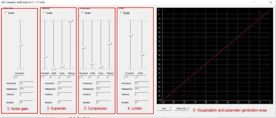
(1) Noise gate: a type of expander that limits signals below a given threshold.
a) Threshold: close the gate dB;
b) Attack: time from closing to opening;
c) Release: time from opening to closing;
d) Hold: holding time of gate opening state;
e) Samples: calculated points, the default is calculating once every 96 points.
(2) Dynamic range expander: attenuates the volume of small sound signals below a given threshold, can make small sound signals sound even quieter.
a) Threshold: extended dB;
b) Width: inflection point excessive smoothing degree, used for smoothing;
c) Ratio: slope;
d) Makeup: gain;
e) Others are the same as above.
(3) Dynamic range compressor: attenuates the volume of loud signals above a given threshold, protecting the hardware and increasing the overall loudness.
(4) Dynamic range limiter: a type of compressor that can limit signals that exceed a given threshold.
After setting the DRC parameters, click "Make Code".
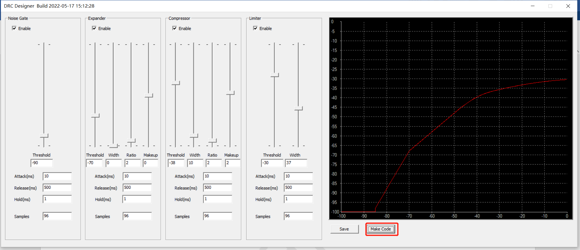
Then the DRC parameter code will be generated, as shown in the following figure:
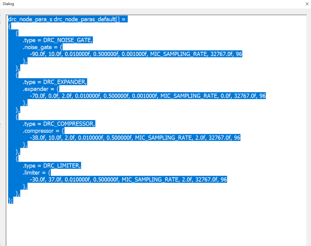
Replacing the default DRC parameter variable with this parameter will implement the import of DRC parameters.
Audio input sources on the Tx end can be I2S, lineIn, DMIC and AMIC. Supports local Lineout to monitor input audio, and can be turned off, controlled by the CODEC_DAC_MONO_MODE macro.
(1) LineIn/AMIC: the default audio input path of the development board, Linein is the jumper cap short connection PIN 34/33.
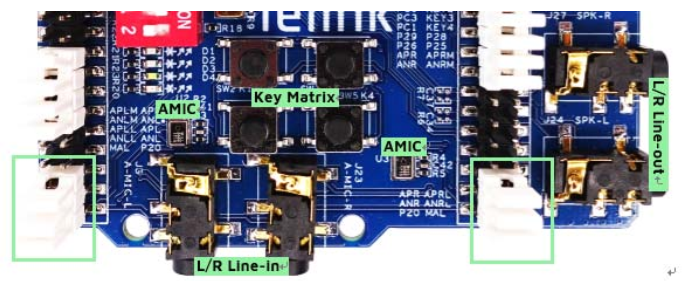
If you need to switch to the analog microphone path, adjust PIN 34/33 jumper cap to PIN 30/29 (Left_Mic is used by default).
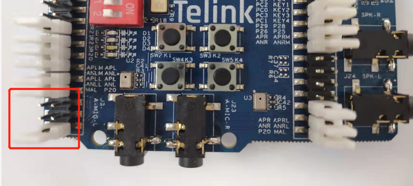
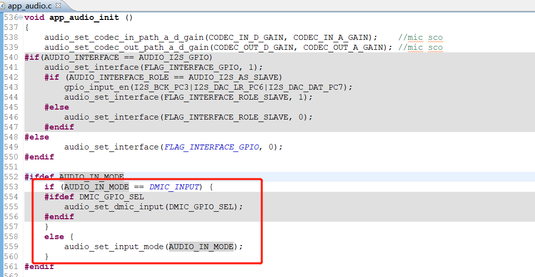
(2) DMIC: To directly use the peripheral audio processing chip to read the digital signal to R9, and set the "AUDIO_IN_MODE" macro to "DMIC_INPUT".
(3) I2S: the default is the host, and the "AUDIO_INTERFACE" macro needs to be set to "AUDIO_I2S_GPIO".
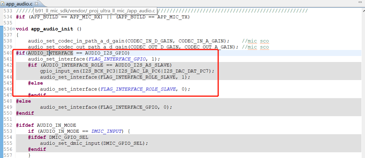
The I2S initialization pins are: PC3 (BCK), PC6 (LR), PC7 (DAT_IN).
(1) Lineout: default audio output. If USB Audio is enabled then USB MIC upstream is added, and at the same time, the USB Audio downstream and the remote Tx audio by the Lineout output will be supported for mixing processing.
(2) I2S: audio output for optional switching, set the "AUDIO_INTERFACE" macro to "AUDIO_I2S_GPIO", and the initialization pins are: PC3(BCK), PC4(LR), PC5(DAT_OUT). If USB Audio is enabled then USB MIC upstream is added, and at the same time, the USB Audio downstream and the remote Tx audio by the I2S output will be supported for mixing processing.
(1) Tx end: the input gain of AMIC, DMIC and Lineout gain can be adjusted, which are controlled by CODEC_IN_A_GAIN(0~20dB), CODEC_IN_D_GAIN(0~43dB), CODEC_OUT_A_GAIN(-19~12dB), CODEC_OUT_D_GAIN(-31~32dB) respectively.
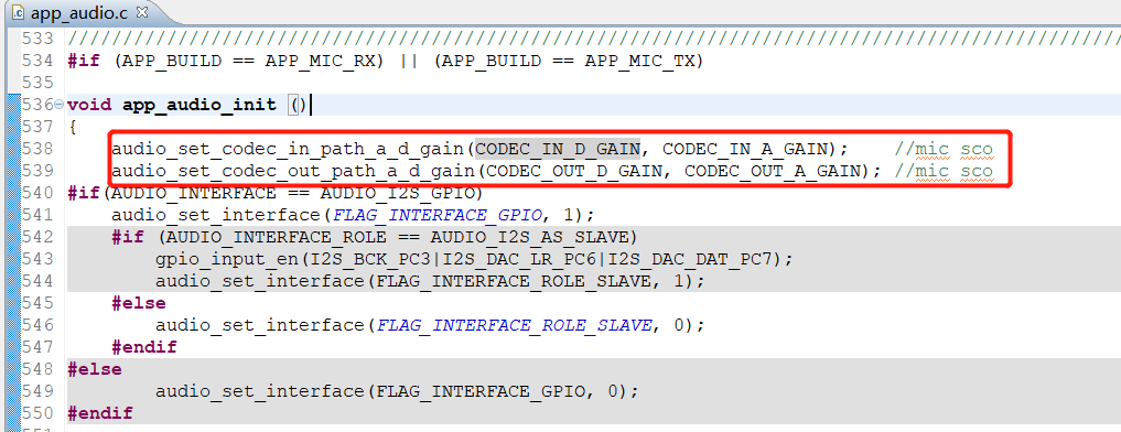
(2) Rx end: only Lineout gain is valid, controlled by CODEC_OUT_A_GAIN and CODEC_OUT_D_GAIN, the initialization interface is the same as above.
The SBC, LC3+ codec algorithms are provided in the SDK, and different needs lead to different encoder configurations, mainly through the following key macros:
(1) MIC_1TO1: used to configure the usage mode, there are 1-to-1 mode and 2-to-1 mode.
(2) MIC_SAMPLING_RATE: used to configure the microphone sample rate, 16K and 48K are available in 2-to-1 mode, and only 48K is supported in 1-to-1 mode.
(3) CODEC_ALGORITHM_SEL: used to configure the encoding algorithm, optional SBC and LC3+.
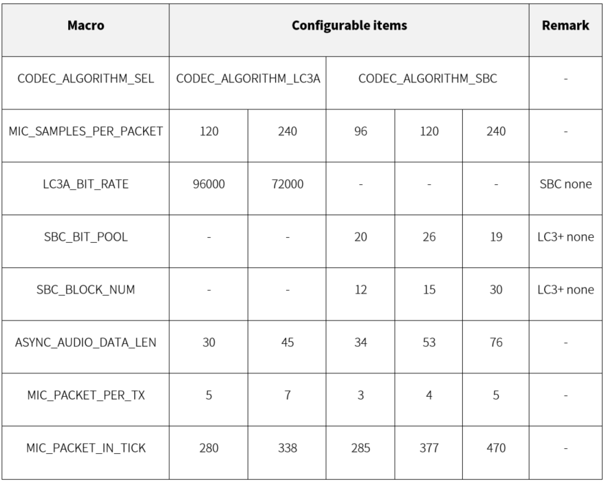
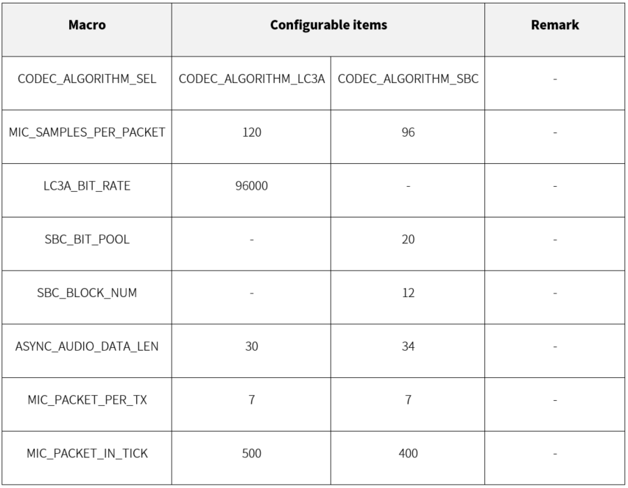
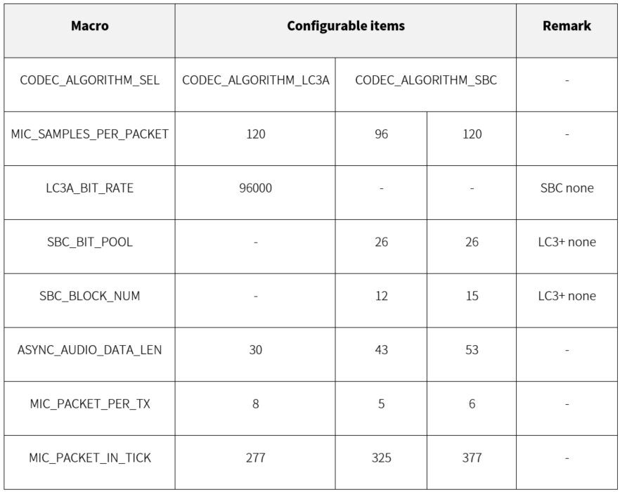
(4) MIC_SAMPLES_PER_PACKET: the number of samples per frame of the microphone, the corresponding values of different modes and different sampling rates are also different, as follows:
a) In 2-to-1 mode, 48K sampling rate: SBC code: 96, 120, 240; LC3+: 120, 240.
b) In 2-to-1 mode, 16K sampling rate: SBC code: 96; LC3+: 120.
c) In 1-to-1 mode, 48K sampling rate: SBC code: 96, 120; LC3+: 120.
(5) SBC_BIT_POOL, SBC_BLOCK_NUM: SBC encoder configuration item, there will be different configurations according to MIC_SAMPLES_PER_PACKET:
a) In 2-to-1 mode, 48K sampling rate: 96 Frame: 20 | 12; 120 Frame: 26 | 15; 240 Frame: 19 | 30.
b) In 2-to-1 mode, 16K sampling rate: 96 Frame: 20 | 12.
c) In 1-to-1 mode, 48K sampling rate: 96 Frame: 26 | 12; 120 Frame: 26 | 15.
(6) LC3A_BIT_RATE: LC3 encoder configuration item, unit bit rate, there will be different configurations according to MIC_SAMPLES_PER_PACKET, among which:
a) In 2-to-1 mode, 48K sampling rate: 120 Frame: 96000; 240 Frame: 72000.
b) In 2-to-1 mode, 16K sampling rate: 120 Frame: 96000.
c) In 1-to-1 mode, 48K sampling rate: 120 Frame: 96000.
(7) ASYNC_AUDIO_DATA_LEN: encoded packet length, in bytes.
(8) MIC_PACKET_PER_TX: the number of times a single Tx is sent.
a) In 1-to-1 mode, MIC_PACKET_PER_TX is the number of MIC_PACKET_NUM Tx transmissions.
b) In 2-to-1 mode, MIC_PACKET_PER_TX = MIC_PACKET_NUM / 2.
(9) MIC_PACKET_IN_TICK: packet sending time, in microseconds, which will affect the final delay.
Users can configure the configuration that meets the project requirements through the orderly combination of the above macros.
The following is the 2-to-1 mode, 48K sampling rate encoding related configuration:
Enable MIC_SAMPLING_RATE_16K macro to enable 2-to-1 mode, 16k sampling rate:
The following is the 1-to-1 mode 48K sample rate, that is, the configuration of the MIC_TX_NUM macro is changed from 2 to 1:
Depending on the pairing mode, encoding, and sampling, Audio's data processing flow, latency, number of packets sent, and transmission distance will vary.
In 2-to-1 mode, the default sampling rate is 48K:
Algorithm Frame Compression ratio Sampling time(ms) Transmission times Latency(ms)
SBC 96 17.71% 2.0 3 7.980
SBC 120 22.08% 2.5 4 8.950
SBC 240 15.83% 5.0 5 13.700
LC3+ 120 12.50% 2.5 5 10.713
LC3+ 240 9.37% 5.0 7 15.525
Table: 2-to-1 mode 48K sampling rate data processing
Configuration 1: The sampling rate is 48k*16bit, each sampling is 2.0ms, producing 96 samples of a total of 192 bytes of raw PCM data. Perform SBC encoding on these 192 bytes, where BIT_POOL: 20, BLOCK_NUM: 12, and get: ((20*12) + 7)/8 + 4 = 34 bytes of data.
Configuration 2: The sampling rate is 48k*16bit, each sampling is 2.5ms, producing 120 samples of a total of 240 bytes of raw PCM data. Perform SBC encoding on these 240 bytes, where BIT_POOL: 26, BLOCK_NUM: 15, and get: ((26*15) + 7)/8 + 4 = 53 bytes of data.
Configuration 3: The sampling rate is 48k*16bit, each sampling is 5.0ms, producing 240 samples of a total of 480 bytes of raw PCM data. Perform SBC encoding on these 480 bytes, where BIT_POOL: 19, BLOCK_NUM: 30, and get: ((19*30) + 7)/8 + 4 = 76 bytes of data.
Configuration 4: The sampling rate is 48k*16bit, each sampling is 2.5ms, producing 120 samples of a total of 240 bytes of raw PCM data. Perform LC3+ encoding on these 240 bytes, BIT_RATE: 96000, and get: (96000*(120/120) + 3199)/3200 = 30 bytes of data.
Configuration 5: The sampling rate is 48k*16bit, each sampling is 5.0ms, producing 240 samples of a total of 480 bytes of raw PCM data. Perform LC3+ encoding on these 480 bytes, BIT_RATE: 72000, and get: (72000*(240/120) + 3199)/3200 = 45 bytes of data.
2-to-1 mode with 16K sampling rate:
Algorithm Frame Compression ratio Sampling time(ms) Transmission times Latency(ms)
SBC 96 17.71% 6.0 7 11.980
LC3+ 120 12.50% 7.5 7 15.713
Table: 2-to-1 mode 16K sampling rate data processing
Configuration 1: The sampling rate is 16k*16bit, each sampling is 6.0ms, producing 96 samples of a total of 192 bytes of raw PCM data. Perform SBC encoding on these 192 bytes, where BIT_POOL: 20, BLOCK_NUM: 12, and get: ((20*12) + 7)/8 + 4 = 34 bytes of data.
Configuration 2: The sampling rate is 16k*16bit, each sampling is 7.5ms, producing 120 samples of a total of 240 bytes of raw PCM data. Perform LC3+ encoding on these 240 bytes, BIT_RATE: 96000, and get: (96000*(120/120) + 3199)/3200 = 30 bytes of data.
Algorithm Frame Compression ratio Sampling time(ms) Transmission times Latency(ms)
SBC 96 22.40% 2.0 5 -
SBC 120 22.08% 2.5 6 -
LC3+ 120 12.50% 2.5 8 -
Table: 1-to-1 mode data processing
Configuration 1: The sampling rate is 48k*16bit, each sampling is 2.0ms, producing 96 samples of a total of 192 bytes of raw PCM data. Perform SBC encoding on these 192 bytes, where BIT_POOL: 26, BLOCK_NUM: 12, and get: ((26*12) + 7)/8 + 4 = 43 bytes of data.
Configuration 2: The sampling rate is 48k*16bit, each sampling is 2.5ms, producing 120 samples of a total of 240 bytes of raw PCM data. Perform SBC encoding on these 240 bytes, where BIT_POOL: 26, BLOCK_NUM: 15, and get: ((26*15) + 7)/8 + 4 = 53 bytes of data.
Configuration 3: The sampling rate is 48k*16bit, each sampling is 2.5ms, producing 120 samples of a total of 240 bytes of raw PCM data. Perform LC3+ encoding on these 240 bytes, BIT_RATE: 96000, and get: (96000*(120/120) + 3199)/3200 = 30 bytes of data.
Published by
Telink Semiconductor
Bldg 3, 1500 Zuchongzhi Rd,
Zhangjiang Hi-Tech Park, Shanghai, China
© Telink Semiconductor
All Rights Reserved
Legal Disclaimer
This document is provided as-is. Telink Semiconductor reserves the right to make improvements without further notice to this document or any products herein. This document may contain technical inaccuracies or typographical errors. Telink Semiconductor disclaims any and all liability for any errors, inaccuracies or incompleteness contained herein.
Copyright © 2022 Telink Semiconductor (Shanghai) Co., Ltd.
Information
For further information on the technology, product and business term, please contact Telink Semiconductor Company www.telink-semi.com
For sales or technical support, please send email to the address of:
Version Change Description
V1.0.0 Initial release

Login (Email)
Password


The new password
Confirm password