B80 BLE Single Connection SDK
SDK Overview
This BLE SDK applies to Telink TLSR820x and TLSR8373 chips, and it supplies demo code for BLE slave single connection development, based on which user can develop his own application program.
Software Architecture
Software architecture for this BLE SDK includes application (APP) layer and BLE protocol stack.
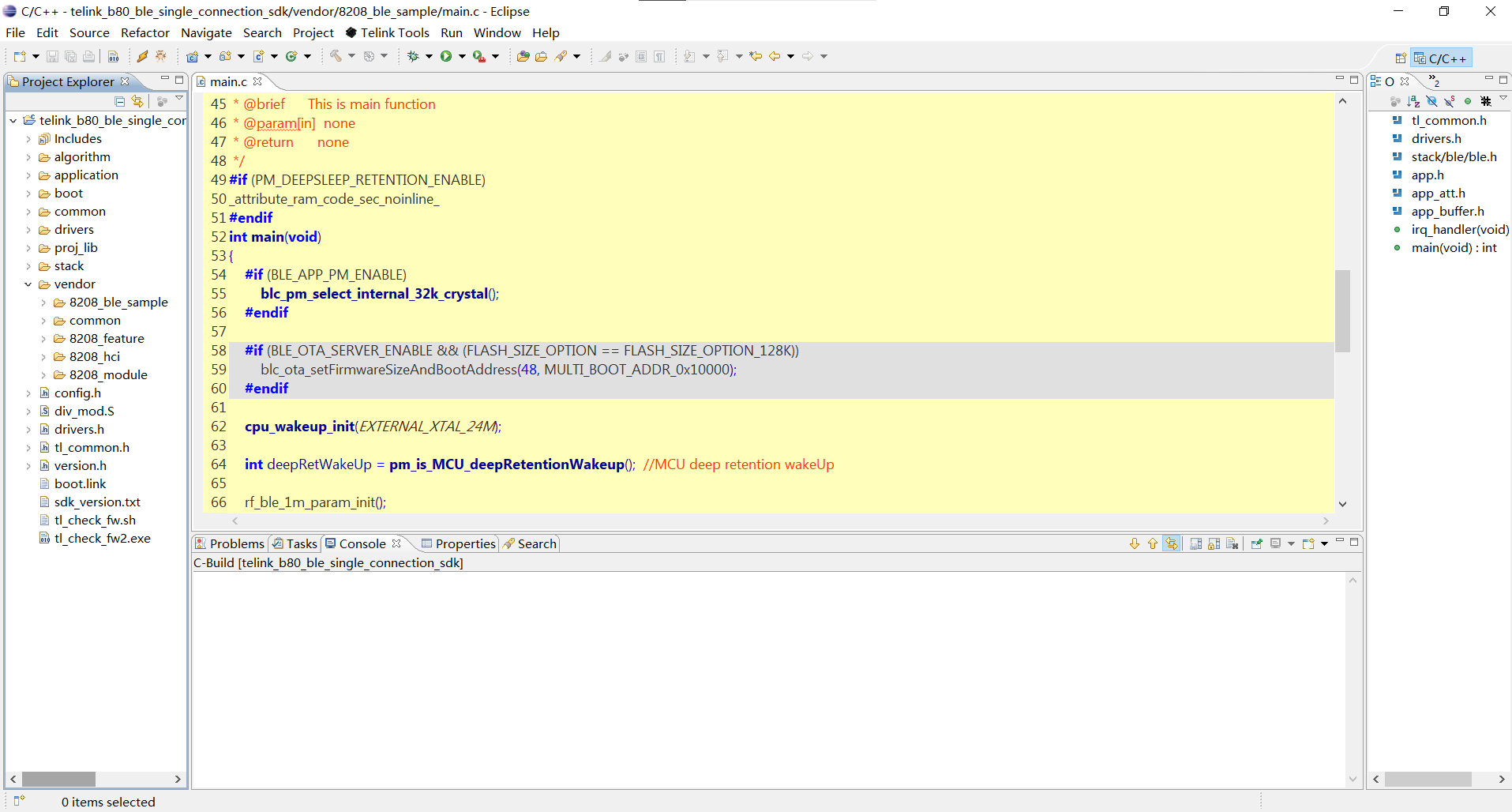
Figure below shows the file structure after the SDK project is imported in IDE, which mainly contains 8 top-layer folders below: "algorithm", "application", "boot", "common", "drivers", "proj_lib", "stack" and "vendor".
-
Algorithm: This folder contains functions related to encryption algorithms.
-
Application: This folder contains general application program.
-
boot: This folder contains software bootloader for chip, i.e., assembly code after MCU power on or deepsleep wakeup, so as to establish environment for C program running.
-
common: This folder contains generic handling functions across platforms, e.g. SRAM handling function, string handling function, and etc.
-
drivers: This folder contains hardware configuration and peripheral drivers closely related to MCU, e.g. clock, flash, i2c, usb, gpio, uart.
-
proj_lib: This folder contains library files necessary for SDK running, e.g. BLE stack, RF driver, PM driver. Since this folder is supplied in the form of library files (e.g. liblt_8208.a), the source files are not open to users.
-
stack: This folder contains header files for BLE stack. Source files supplied in the form of library files are not open to users.
-
vendor: This folder contains user application-layer code.
main.c
The “main.c” file includes main function entry, system initialization functions and endless loop “while(1)”. It’s not recommended to make any modification to this file.
#if (PM_DEEPSLEEP_RETENTION_ENABLE)
_attribute_ram_code_sec_noinline_
#endif
int main(void)
{
    #if (BLE_APP_PM_ENABLE)
        blc_pm_select_internal_32k_crystal();
    #endif

    #if (BLE_OTA_SERVER_ENABLE && (FLASH_SIZE_OPTION == FLASH_SIZE_OPTION_128K))
        blc_ota_setFirmwareSizeAndBootAddress(48, MULTI_BOOT_ADDR_0x10000);
    #endif

    cpu_wakeup_init(EXTERNAL_XTAL_24M);

    int deepRetWakeUp = pm_is_MCU_deepRetentionWakeup();  //MCU deep retention wakeUp

    rf_ble_1m_param_init();

    clock_init(SYS_CLK_TYPE);

    gpio_init( !deepRetWakeUp );  //analog resistance will keep available in deepSleep mode, so no need initialize again

    /* load customized freq_offset CAP value and TP value. */
    blc_app_loadCustomizedParameters();

    #if FIRMWARES_SIGNATURE_ENABLE
        blt_firmware_signature_check();
    #endif

    #if (PM_DEEPSLEEP_RETENTION_ENABLE)
        if( deepRetWakeUp ){
            user_init_deepRetn ();
        }
        else
    #endif
        {
        #if(BATT_CHECK_ENABLE)
            blc_app_loadADCParameters();
        #endif
            user_init_normal ();
        }

    #if (MODULE_WATCHDOG_ENABLE)
        wd_set_interval_ms(WATCHDOG_INIT_TIMEOUT,CLOCK_SYS_CLOCK_1MS);
        wd_start();
    #endif

    irq_enable();

    while (1) {
        #if (MODULE_WATCHDOG_ENABLE)
            wd_clear(); //clear watch dog
        #endif

        main_loop ();
    }
}
app_config.h
The user configuration file “app_config.h” serves to configure parameters of the whole system, including parameters related to BLE, GPIO, PM (low-power management), and etc. Parameter details of each module will be illustrated in following sections.
Application File
-
"app.c": User file for BLE protocol stack initialization, data processing and low power management.
-
"app_att.c": configuration files for services and profiles. Based on Telink Attribute structure, as well as Attributes such as GATT, standard HID, proprietary OTA and MIC, user can add his own services and profiles as needed.
-
"app_buffer.c": Used to configure ACL RX FIFO, ACL TX FIFO, L2CAP RX Buffer, etc.
-
"app_ui.c": Processing files for user tasks such as buttons, OTA, etc.
BLE Stack Entry
There are two entry functions in BLE stack code of Telink BLE SDK.
(1) BLE related interrupt handling entry "blc_sdk_irq_handler" in "irq_handler" function of the main.c file.
_attribute_ram_code_ void rf_irq_handler (void)
{
……
blc_sdk_irq_handler ();
……
}
(2) BLE logic and data handling entry "blc_sdk_main_loop" in "main_loop" of the application file.
void main_loop (void)
{
///////////////////// BLE entry ////////////////////////////
    blc_sdk_main_loop();
////////////////////// UI entry ////////////////////////////
……
////////////////////// PM process ////////////////////
……
}
Applicable IC
The following IC models are applicable, they belong to B80 series with the same core, among which 8208A/8208B/8208C hardware modules are basically the same, only slightly different in Flash. The details are shown in the table below.
| IC | Flash size |
|---|---|
| 8208A | no built-in Flash |
| 8208B | built-in 128 kB |
| 8208C | built-in 512 kB |
Because the difference between the above 3 ICs is mainly the Flash, the other parts are the same, and the SDK file structure is completely shared except for the differences between the SDK/boot/boot script (i.e. software bootloader file) and the boot.link file.
Software Bootloader
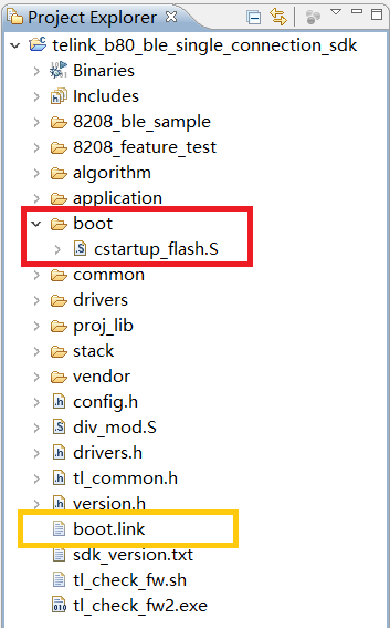
The software bootloader file is stored in the boot directory, as shown below:
Demo Codes
Telink BLE SDK provides users with multiple BLE Slave Demo.
Users can observe intuitive effects by running the software and hardware demo. Users can also modify the demo code to complete their own application development. Demo codes path is shown as below.

BLE slave demos and their differences are shown in the table below.
| Demo | Stack | Application | MCU Function |
|---|---|---|---|
| 8208 hci | BLE controller | No | BLE controller, only Advertising and one Slave |
| 8208 module | BLE controller + host | Application is on the host MCU | BLE transmissive module |
| 8208 ble sample | BLE controller + host | The simplest slave demo for broadcast and connection | Host MCU |
| 8208 feature | BLE controller + host | Collection of various features | Host MCU |
8208 hci is a BLE slave controller that provides USB/UART based HCI, and communicates with other MCU host to form a complete BLE slave system.
8208 module is only used as a BLE transmissive module to communicate with the host MCU through UART interface, and the general application code is written in the other host MCU.
8208 module realizes the function of controlling the related state change through the transmissive module.
8208 ble sample is a simplified slave demo that can be paired and connected with standard IOS/android devices..
Feature Demo and Driver Demo
8208_feature_test gives demo code for some common BLE-related features, users can refer to these demos to complete their own functional implementation, see code for details. The BLE section of the document will introduce all the features.
The macro "FEATURE_TEST_MODE" is optionally defined in feature_config.h in the 8208_feature_test project to switch to different feature demos.
MCU Basic Modules
MCU Address Space
MCU Address Space Allocation
The MCU address space allocation is shown in the figure below.
The Telink B80 MCU has a maximum addressable space of 16M bytes.
- The 8M space from 0 to 0x7FFFFF is the program space, i.e. the maximum program capacity is 8M bytes.
- 0x800000 to 0xFFFFFF is the external device space: 0x800000\~0x80FFFF is the register space; 0x840000\~0x84FFFF is the 64K SRAM space.
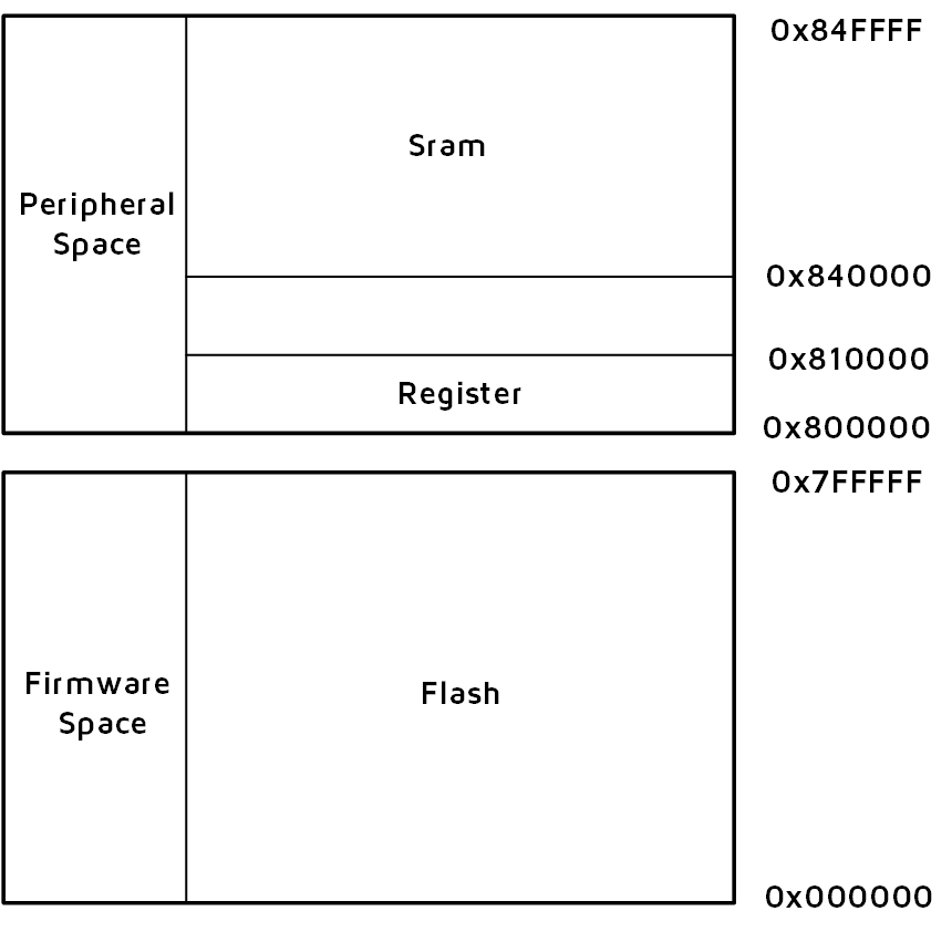
When the B80 MCU is physically addressed, address line BIT (23) is used to distinguish between program space/peripheral space.
- When this address is 0, access the program space.
- When this address is 1, access the peripheral space.
When the addressing space is peripheral space (BIT(23) is 1), address line BIT(18) is used to distinguish between Register and SRAM.
- When this address is 0, access the register.
- When this address is 1, access the SRAM.
SRAM Space Allocation
The space allocation of B80 SRAM is closely related to the deepsleep retention function in the low-power management section, so please master the knowledge about deepsleep retention first.
(1) SRAM and Firmware Space
The allocation of SRAM space in the MCU address space is further explained.
The 16kB SRAM address space ranges from 0x840000 to 0x844000, and the corresponding SRAM and Firmware space allocation is shown in the figure below.
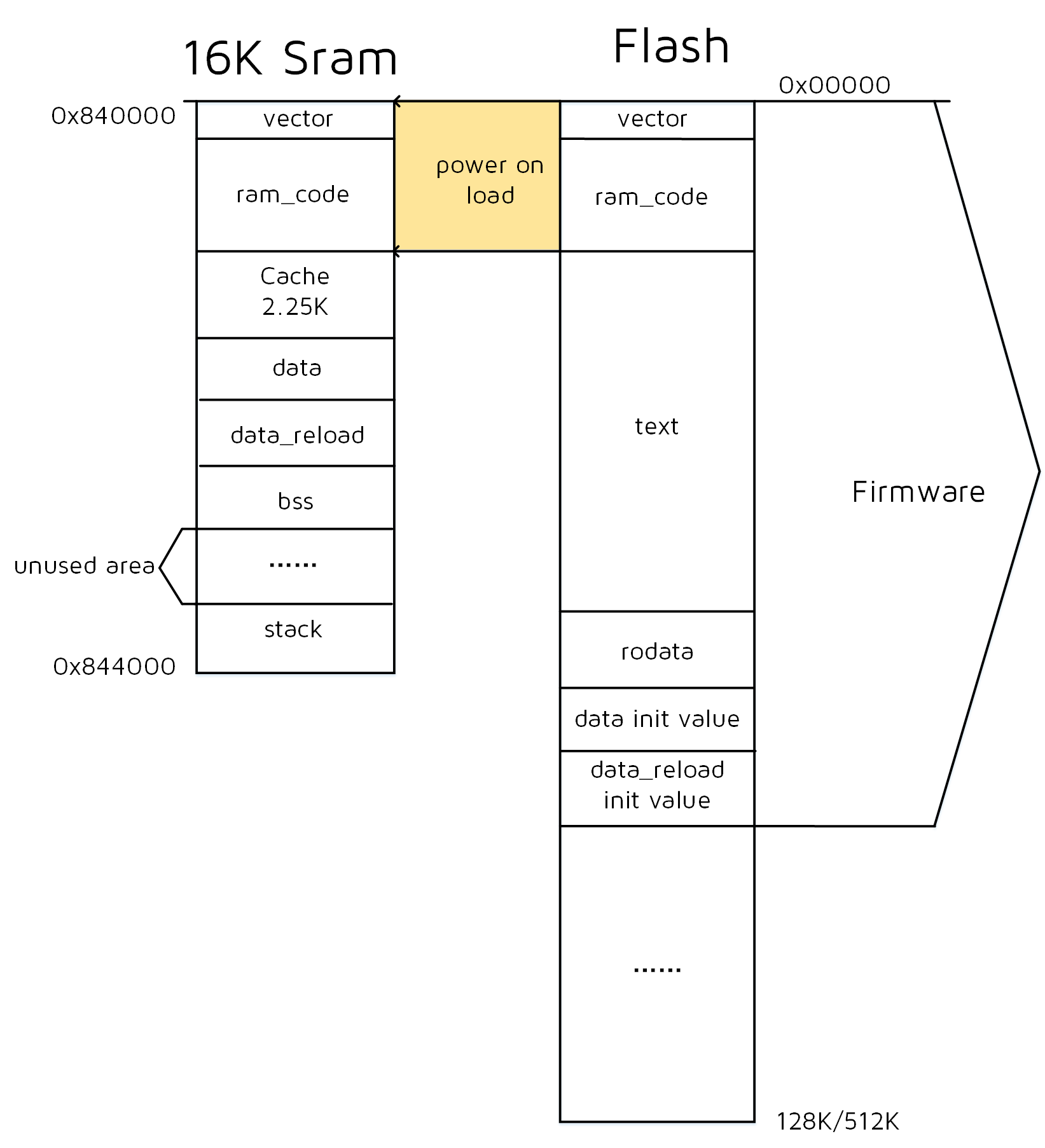
The files related to SRAM space allocation in SDK are boot.link and cstartup_flash.S.
The Firmware in Flash includes vector, ramcode, retention_data, text, rodata, data init value and data_reload init value.
SRAM includes vector, ramcode, Cache, data, data_reload, bss, stack and unused sram area.
The vector/ramcode in SRAM is a copy of vector/ramcode in Flash.
(a) vectors and ram_code
The "vectors" segment is the program corresponding to the assembly file cstartup_flash.S, which is the software bootloader.
The "ramcode" segment is the code in the Flash Firmware that needs to be resident in RAM, corresponding to all functions in the SDK with the keyword "attribute_ram_code" or "attribute_ram_code_sec_noinline", such as flash_send_cmd function.
_attribute_ram_code_sec_noinline_ static void flash_send_cmd(unsigned char cmd);
There are two reasons for functions to be resident in memory.
One is that some functions must be resident in memory because they involve timing multiplexing with the four pins of the Flash MSPI, and if they are put into flash there will be timing conflicts that will cause crashes, such as all functions related to flash operations.
The second is that the function in the ram is executed every time it is called without re-reading from flash, which can save time. So for some functions with execution time requirements can be put into the resident memory to improve execution efficiency. SDK will be BLE timing-related functions often to be executed resident in memory, greatly reducing the execution time, and finally achieve power saving.
If you need to make a function resident in memory, you can follow flash_send_cmd above and add the keyword to your own function, then you can see the function in the ramcode segment in the list file after compilation.
Both the vector and ramcode in Firmware need to be moved to ram when the MCU is powered up. After compilation, the size of these two parts are added together as ramcode_size. The ramcode_size is a variable value that the compiler can recognize, and its calculation is implemented in boot.link, as shown below. The compiled result ramcode_size is equal to the size of all codes of vector and ramcode.
    . = 0x0;
        .vectors :
        {
        *(.vectors)
        *(.vectors.*)
        }
        .ram_code :
        {
        *(.ram_code)
        *(.ram_code.*)
        }
    PROVIDE(_ramcode_size_ = . );//Calculate actual ramcode size(vector + ramcode)
(b) Cache
The Cache is the MCU's instruction cache and must be configured as a section of Sram to function properly. The Cache size is fixed and consists of 256 bytes of tag and 2048 bytes of instructions cache, totaling 0x900 = 2.25K.
The code of resident in memory can be read and executed directly from SRAM, but the code in firmware that can be resident in SRAM is only partial, and most of the rest is still in flash. According to the principle of program locality, a part of flash code can be stored in Cache, and if the current code to be executed is in Cache, it can be directly read from Cache and executed; if it is not in Cache, the code can be read from flash and moved to Cache, and then read from Cache and executed.
The "text" segment of the Firmware is not placed in the SRAM. This part of the code conforms to the principle of program locality and needs to be loaded into the Cache to be executed.
The Cache size is fixed at 2.25K, its starting address in SRAM is configurable.
(c) data
The "data" segment is a global variable in SRAM that holds the program that has been initialized, i.e., the global variable with non-zero initial value. This part will only be reinitialized after power-on or wake-up from deep sleep, and maintain the value before sleep during deepsleep retention and suspend.
The "data" segment follows the Cache, and the starting address is the end address of the Cache. The following is the code in boot.link, which directly defines the address at the beginning of the "data" segment on SRAM:
     . = (0x840000 + ((0x900 + _ramcode_size_align_256_) * __LOAD_FLASH) + (0x400 * __LOAD_DUT) + (_dstored_ * __LOAD_RAM));
    .data :
The "data" segment is a global variable that is initialized and its initial value needs to be stored in flash in advance, i.e. the "data initial value" in the Firmware shown in the figure.
(d) data_reload
In order to save the boot time of retention wake-up, the "data" and "bss" segments in 8208 are set to retention, and the retention wake-up is no longer initialized. On the other hand, some variables need to be initialized when the retention wake-up, so we add the "data_reload" segment. The characteristic of this segment is that it will be reinitialized after the retention wake-up and will no longer retain the value before sleep.
The "data_reload" segment follows the "data" segment, and the starting address is the end address of the "data" segment. The following is the code in boot.link, which directly defines the address at the beginning of the "data_reload" segment on SRAM:
    PROVIDE(_rstored_ = _dstored_ + _end_data_ - _start_data_);

    .data_reload :
    AT ( _rstored_ )
The "data_reload" segment is a global variable that is initialized and its initial value needs to be stored in flash in advance, i.e. the "data_reload init value" in the Firmware shown in the figure.
(e) bss
The "bss" segment is a global variable in SRAM that holds the program uninitialized, i.e., the global variable with an initial value of 0. This part will only be reinitialized after power-on or wake-up from deep sleep, and maintain the value before sleep during deepsleep retention and suspend.
The "bss" segment follows the "data_reload" segment, and the starting address is the end address of the "data_reload" segment. The following is the code in boot.link, which directly defines the address at the beginning of the "bss" segment on SRAM:
    PROVIDE(_data_reload_end_ = . );
    ……
    .bss :
    {
    . = (((. + 3) / 4)*4);
    PROVIDE(_start_bss_ = .);
    ……
(f) stack / unused area
For 16K SRAM, the "stack" starts from the highest address 0x844000, and its direction is from bottom to top, that is, the stack pointer SP decreases when the data is pushed into the stack and increases when the data is popped out of the stack.
By default, the SDK library uses a stack size of no more than 256 bytes, but since the stack size depends on the address of the deepest position of the stack, the final stack usage is related to the user's upper-level program design. If the user uses a troublesome recursive function call, or uses a relatively large local array variable in the function, or other situations that may cause the stack to be deeper, the final stack size will increase.
When the user uses more sram, he needs to know exactly how much stack his program uses. This cannot be analyzed by the list file, but only by letting the application run and making sure it runs all the codes in the program that may use deeper stack, then reset the MCU and read the sram space to determine the amount of stack used.
The "unused area" is the space left between the end of the bss segment and the deepest address of the stack. Only when this space exists, it means that stack is not in conflict with bss and there is no problem with Sram usage. If the deepest part of the stack overlaps with the bss segment, then there is not enough Sram.
Through the list file, we can find out the address of the end of the bss segment, which also determines the maximum space left for stack, and the user needs to analyze whether this space is enough, and in combination with the deepest address of stack mentioned above, we can know whether the use of Sram is exceeded. The analysis method will be given in the following demo.
(g) text
The "text" segment is a collection of all non-ram_code functions in the Flash Firmware. If "_attribute_ram_code_" or "attribute_ram_code_sec_noinline" is added to the function in the program, it will be compiled into the ram_code segment, while all other functions without this keyword will be compiled into the "text" segment. In general, the "text" segment is the largest space in the firmware, much larger than the size of Sram, so it is necessary to load the code to be executed into the Cache first through the cache function of the Cache before it can be executed.
(h) rodata /data init value /data_reload init value
Except for vector, ram_code and text, the remaining data in Flash Firmware are "rodata" segment, "data init value" and "data_reload init value".
The "rodata" segment is the readable and unwritable data defined in the program, and is a variable defined by the keyword "const". For example, the ATT table in Slave.
static const attribute_t my_Attributes[] = ……
The user can see in the corresponding list file that "my_Attributes" is in the rodata segment.
The "data" segment introduced earlier is a global variable that has been initialized in the program, for example, the global variable is defined as follows.
int testValue = 0x1234;
Then the compiler will store the initial value 0x1234 in the "data initial value", and when power on or deepsleep wakes up, it will copy the initial value to the memory address corresponding to testValue.
The "data_reload" segment introduced earlier is a global variable defined in the program as the retention wake-up reinitialization, for example, the global variable is defined as follows.
_attribute_data_reload_ int reloadValue = 0x1234;
Then the compiler will store the initial value 0x1234 in the "data_reload init value", and when running the bootloader, it will copy the initial value to the memory address corresponding to reloadValue.
(2) List File Analysis Demo
Here, the default configuration of 8208 ble sample is taken as an example, combined with "Sram space allocation & Firmware space allocation" to analyze.
In the following analysis, there will be several screenshots, all from boot.link, cstartup_flash.S, 8208 ble sample.bin and 8208 ble sample.list, please find the file to find the corresponding location of the screenshots by yourself.
The distribution of each section in the list file is shown in the following figure (note the Algn byte alignment):
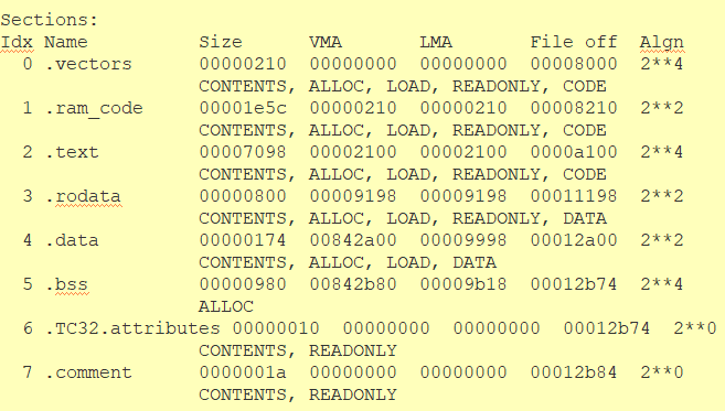
According to the section analysis, below lists the information you need to know, detailed introduction will be introduced later.
(a) vectors: start from Flash 0, Size is 0x210, the end address is calculated as 0x210;
(b) ram_code: start from Flash 0x210, Size is 0x1e5c, the end address is calculated as 0x2100;
(c) text: start from Flash 0x2100, Size is 0x7098, the end address is calculated as 0x9198;
(d) rodata: start from Flash 0x9198, Size is 0x800, the end address is calculated as 0x9998;
(e) data: start from Sram 0x842a00, Size is 0x174, the end address is calculated as 0x842b74;
(f) bss: start from Sram 0x842b80 (not starting from 0x842b74 for alignment reasons), Size is 0x980, the end address is calculated as 0x843500。
Combined with the previous introduction, the remaining Sram space is 0x844000 – 0x843500 = 0xb00 = 2816 bytes, minus the 256 bytes needed for stack, leaving 2560 bytes.
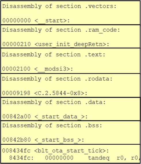
The above figure shows the starting address of some of the sections in the list file after the search for "section", combined with this figure and the above "list file section statistics", the analysis is as follows.
(a) vector:
The "vectors" segment in the flash firmware starts at address 0, ends at address 0x210, and size is 0x210. After power-on move to Sram, the address on Sram is 0x840000 ~ 0x840210.
(b) ram_code:
The "ram_code" segment starts at 0x210 and ends at 0x2100 in the flash firmware. After the power-on move to Sram, the address on Sram is 0x840210 ~ 0x842100.
(c) Cache:
The Cache address range in Sram is 0x842100 ~ 0x842a00. The information about Cache will not be reflected in the list file.
(d) text:
The "text" segment starts at 0x2100 and ends at 0x9198 in the flash firmware, the Size is 0x9198 – 0x2100 = 0x7098, which is the same as the data in the previous Section statistics.
(e) rodata:
The starting address of the "rodata" segment is the end address of text 0x9198, and the end address is 0x9998.
(f) data:
The starting address of the "data" segment on the Sram is the end address of the Cache 0x842a00, and the size given in the Section statistics section of the list file is 0x174. The "data" segment ends at address 0x842b74 on the SRAM.
(g) bss:
The starting address of the "bss" segment on the Sram is the end address of the "data" segment 0x842b80 (16-byte alignment), and the size given in the Section statistics section of the list file is 0x980. The "bss" segment ends at address 0x843500 on the SRAM.
The remaining Sram space is 0x844000 – 0x843500 = 0xb00 = 2816 bytes, minus the 256 bytes needed for stack, leaving 2560 bytes.
MCU Address Space Access
Access to the 0x000000 - 0xFFFFFF address space in the program is divided into the following two situations.
(1) Peripheral Space R/W Operation
Read and write operations in the peripheral space (register and sram) are implemented directly with pointer access.
    u8  x = *(volatile u8*)0x800066;  //read value of register 0x66
     *(volatile u8*)0x800066 = 0x26;  //assign value to register 0x66
    u32 y = *(volatile u32*)0x840000;      //read value of sram 0x40000-0x40003
    *(volatile u32*)0x840000 = 0x12345678; //assign value to sram 0x40000-0x40003
The program uses the functions write_reg8, write_reg16, write_reg32, read_reg8, read_reg16, read_reg32 to read and write to the peripheral space, which are essentially pointer operations. For more information, please refer to drivers/bsp.h.
Note the operation similar to write_reg8(0x40000)/ read_reg16(0x40000) in the program, which is defined as shown below, from which the 0x800000 offset is automatically added (address line BIT(23) is 1), so the MCU can ensure that it is accessing the Register/Sram space and not going to flash space.
#define REG_BASE_ADDR           0x800000

#define REG_ADDR8(a)            (*(volatile unsigned char*) (REG_BASE_ADDR | (a)))
#define REG_ADDR16(a)           (*(volatile unsigned short*)(REG_BASE_ADDR | (a)))
#define REG_ADDR32(a)           (*(volatile unsigned long*) (REG_BASE_ADDR | (a)))

#define write_reg8(addr,v)      (*(volatile unsigned char*)  (REG_BASE_ADDR | (addr)) = (unsigned char)(v))
#define write_reg16(addr,v)     (*(volatile unsigned short*) (REG_BASE_ADDR | (addr)) = (unsigned short)(v))
#define write_reg32(addr,v)     (*(volatile unsigned long*)  (REG_BASE_ADDR | (addr)) = (v))

#define read_reg8(addr)         (*(volatile unsigned char*) (REG_BASE_ADDR | (addr)))
#define read_reg16(addr)        (*(volatile unsigned short*)(REG_BASE_ADDR | (addr)))
#define read_reg32(addr)        (*(volatile unsigned long*) (REG_BASE_ADDR | (addr)))
Note here a memory alignment problem: If you use a pointer to 2 bytes/4 bytes to read or write peripheral space, make sure the address is 2 bytes/4 bytes aligned, if not aligned, data read/write errors will occur. The following two are errors.
u16  x = *(volatile u16*)0x840001;     //0x840001 is not 2-byte aligned
*(volatile u32*)0x840005 = 0x12345678;  //0x840005 is not 4-byte aligned
Modify to the correct read/write operation.
u16  x = *(volatile u16*)0x840000;     //0x840000 is 2-byte aligned
*(volatile u32*)0x840004 = 0x12345678;  //0x840004 is 4-byte aligned
(2) Flash Operation
This section is detailed in Chapter 8, Flash.
SDK Flash Space Allocation
This section is detailed in Chapter 8, Flash.
Clock Module
System Clock & System Timer
The system clock is the clock used by the MCU to execute the program.
The system timer is a read-only timer that provides a time reference for timing control of the BLE and is also available to the user.
On Telink's previous generation ICs (826x series), the System Timer clock is from the system clock, while on the B80 series ICs, the System Timer and system clock are independently separated. As shown in the diagram below, the System Timer is 16MHz obtained by dividing the external 24MHz Crystal Oscillator.
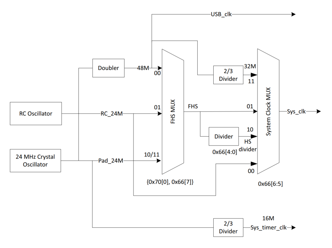
As you can see, the system clock can be multiplied to 48M by the external 24M crystal oscillator through the "doubler" circuit and then divided to get 16M, 24M, 32M, 48M, etc. This type of clock is called crystal clock (such as 16M crystal system clock, 24M crystal system clock). It can also be processed by the IC internal 24M RC Oscillator to get 24M RC clock, 32M RC clock, 48M RC clock and so on. This category is called RC clock (BLE SDK does not support RC clock).
In the BLE SDK we recommend to use crystal clock.
To configure the system clock, call the following API during initialization and select the clock corresponding to the clock in the enumeration variable SYS_CLK_TYPEDEF definition.
void clock_init(SYS_CLK_TypeDef SYS_CLK)
Since the System Timer of B80 series chip is different from the system clock, users need to know whether the clock of each hardware module on MCU is from system clock or System Timer. Let's take the case where the system clock is 24M crystal to illustrate, at this time the system clock is 24M and the System Timer is 16M.
In the file app_config.h, the system clock and the corresponding s, ms and us are defined as follows.
#define CLOCK_SYS_CLOCK_HZ      24000000
enum{
        CLOCK_SYS_CLOCK_1S = CLOCK_SYS_CLOCK_HZ,
        CLOCK_SYS_CLOCK_1MS = (CLOCK_SYS_CLOCK_1S / 1000),
        CLOCK_SYS_CLOCK_1US = (CLOCK_SYS_CLOCK_1S / 1000000),
};
All hardware modules whose clock source is system clock can only use the above CLOCK_SYS_CLOCK_HZ, CLOCK_SYS_CLOCK_1S, etc. when setting the clock of the module; in other words, if the user sees that the clock setting in the module uses the above definitions, it means that the clock source of the module is system clock.
If the PWM driver PWM period and duty cycle are set as follows, it means that the PWM clock source is system clock.
pwm_set_cycle_and_duty(PWM0_ID, (u16) (1000 * CLOCK_SYS_CLOCK_1US), (u16) (500 * CLOCK_SYS_CLOCK_1US) );
The System Timer is a fixed 16M, so for this timer, the SDK code uses the following values for s, ms and us.
//system timer clock source is constant 16M, never change
enum{
        CLOCK_16M_SYS_TIMER_CLK_1S =  16000000,
        CLOCK_16M_SYS_TIMER_CLK_1MS = 16000,
        CLOCK_16M_SYS_TIMER_CLK_1US = 16,
};
The following APIs in SDK are some operations related to System Timer, so when it comes to these API operations, they all use the above similar to "CLOCK_16M_SYS_TIMER_CLK_xxx" to represent the time.
void sleep_us (unsigned long microsec);
unsigned int clock_time(void);
int clock_time_exceed(unsigned int ref, unsigned int span_us);
#define ClockTime           clock_time
#define WaitUs              sleep_us
#define WaitMs(t)           sleep_us((t)*1000)
Since the System Timer is the reference for BLE timing, all BLE time-related parameters and variables in the SDK are expressed as "CLOCK_16M_SYS_TIMER_CLK_xxx" when it comes to the time.
System Timer Usage
After the initialization of sys_init in the main function is completed, the System Timer starts to work, and the user can read the value of the System Timer counter (referred to as System Timer tick).
The System Timer tick is incremented by one every clock cycle, and its length is 32bit, that is, every 1/16 us plus 1, the minimum value is 0x00000000, and the maximum value is 0xffffffff. When the System Timer starts, the tick value is 0, and the time required to reach the maximum value of 0xffffffff is: (1/16) us * (2^32) approximately equal to 268 seconds, and the System Timer tick makes one cycle every 268 seconds.
The system tick will not stop when the MCU is running the program.
The reading of System Timer tick can be obtained through the clock_time() function:
u32 current_tick = clock_time();
The entire BLE timing of the BLE SDK is designed based on the System Timer tick. This System Timer tick is also used extensively in the program to complete various timing and timeout judgments. It is strongly recommended that users use this System Timer tick to implement some simple timing and timeout judgments.
For example, to implement a simple software timing. The realization of the software timer is based on the query mechanism. Because it is implemented through query, it cannot guarantee real-time performance and readiness. It is generally used for applications that are not particularly demanding on error. Implementation:
(1) Start timer: set a u32 variable, read and record the current System Timer tick.
u32 start_tick = clock_time(); // clock_time() returns System Timer tick value
(2) Constantly inquire whether the difference between the current System Timer tick and start_tick exceeds the time value required for timing in the program. If it exceeds, consider that the timer is triggered, perform corresponding operations, and clear the timer or start a new round of timing according to actual needs.
Assuming that the time to be timed is 100 ms, the way to query whether the time is reached is:
if( (u32) ( clock_time() - start_tick) > 100 * CLOCK_16M_SYS_TIMER_CLK_1MS)
Since the difference is converted to the u32 type, the limit of the system clock tick from 0xffffffff to 0 is solved.
In fact, in order to solve the problem of conversion to u32 caused by different system clocks, the SDK provides a unified calling function. Regardless of the system clock, the following functions can be used to query and judge:
if( clock_time_exceed(start_tick, 100 * 1000)) //unit of the second parameter is us
Note:
Since the 16MHz clock takes 268 seconds for one cycle, this query function is only applicable to the timing within 268 seconds. If it exceeds 268 seconds, you need to add a counter to accumulate in the software (not introduced here).
Application example: after 2 seconds when A condition is triggered (only once), the program performs B() operation.
u32  a_trig_tick;
int  a_trig_flg = 0;
while(1)
{
        if(A){
            a_trig_tick = clock_time();
            a_trig_flg = 1;
        }
        if(a_trig_flg && clock_time_exceed(a_trig_tick,2 *1000 * 1000)){
            a_trig_flg = 0;
            B();
        }
}
GPIO Module
The description of GPIO module please refer to drivers/gpio.h, gpio_default.h, gpio.c to understand, all code is provided in source code form.
The code involves the operation of registers, please refer to the datasheet to understand.
GPIO Definition
B80 series chips support up to 5 groups of 38 GPIOs: GPIO_PA0 ~ GPIO_PA7, GPIO_PB0 ~ GPIO_PB7, GPIO_PC0 ~ GPIO_PC7, GPIO_PD0 ~ GPIO_PD7, GPIO_PE0 ~ GPIO_PE3 and GPIO_PF0 ~ GPIO_PF1.
Note:
There are 36 GPIOs in the core part of the IC, however some GPIOs may not be pinned out in the different packages of each IC, therefore please refer to the actual GPIO pins in the package of the IC when using GPIOs.
When you need to use GPIO in your program, you must define it as written above, see drivers/gpio.h for details.
Note:
The 7 GPIOs are special and need attention:
a)4 GPIOs of MSPI, these 4 GPIOs are the main SPI bus in MCU system bus for read/write flash operation, power on default for spi state, user can never operate them, program can not use them. These 4 GPIOs are PE0, PE1, PE2 and PE3.
b)SWS (Single Wire Slave), used for debug and burning firmware, power on default for SWS state, it is generally not used in the program. The SWS pin in B80 chip is PA3.
c)DM and DP, power on default GPIO state. DM and DP need to be used when USB function is needed; when USB is not needed, it can be used as GPIO. The DM and DP pin of B80 are PA1 and PA2.
GPIO State Control
Only the most basic GPIO states that users need to know are listed here.
(1) func (function configuration: special function/general GPIO), if you need to use the input and output function, you need to configure it as general GPIO.
void gpio_set_func(GPIO_PinTypeDef pin, gpio_func_e func);
The pin is defined for GPIO, the same as below. For func you can choose AS_GPIO or other special functions.
(2) ie (input enable)
void gpio_set_input_en(GPIO_PinTypeDef pin, unsigned int value);
value: 1 and 0 means enable and disable respectively.
(3) datai (data input): When the input enable is on, this value is the current level of this GPIO pin, which is used to read the external voltage.
static inline _Bool gpio_read(GPIO_PinTypeDef pin);
Read low voltage returns a value of 0; read high voltage returns a value of 1.
if( !gpio_read(GPIO_PA0) ) //Determining high and low voltages
(4) oe (output enable)
static inline void gpio_set_output_en(GPIO_PinTypeDef pin, unsigned int value);
value: 1 and 0 means enable and disable respectively.
(5) datao (data output): When the output enable is on, the value is 1 to output high, 0 to output low.
static inline void gpio_write(GPIO_PinTypeDef pin, unsigned int value);
(6) For the internal analog pull-up and pull-down resistor configuration, there are 3 analog resistors: 1Mohm pull-up, 10Kohm pull-up and 100Kohm pull-down, and 4 configurable states: 1Mohm pull-up, 10Kohm pull-up, 100Kohm pull-down and float state.
void gpio_setup_up_down_resistor(GPIO_PinTypeDef gpio, GPIO_PullTypeDef up_down);
The four configurations of up_down:
typedef enum {
    PM_PIN_UP_DOWN_FLOAT    = 0,
    PM_PIN_PULLUP_1M        = 1,
    PM_PIN_PULLDOWN_100K    = 2,
    PM_PIN_PULLUP_10K       = 3,
}GPIO_PullTypeDef;
In the deepsleep and deepsleep retention states, the GPIO input and output states are all disabled, but the analog pull-up and pull-down resistors are still valid.
Note:
The following sequence is required when making GPIO function change configurations.
a)The beginning function is GPIO, then you need to configure the required function MUX first, and then disable the GPIO function.
b)The beginning function is IO, you need to change to GPIO output, first set the corresponding IO output value and OEN, and then finally enable GPIO function.
c)The beginning function is IO, you need to change to GPIO input and IO pullup, first set output to 1, OEN to 1 (corresponding to PA and PD), second set pullup to 1 (corresponding to PB and PC), and finally enable GPIO function.
d)Set pullup to 1 (corresponding to PB and PC) and IO not pull up, first set output to 0, OEN to 1 (corresponding to PA and PD), then set pullup to 0 (corresponding to PB and PC), and finally enable GPIO function.
GPIO configuration application examples:
(1) Configure GPIO_PA4 as output state and output high level.
gpio_set_func(GPIO_PA4, AS_GPIO) ;  // PA4 is GPIO by default, you can leave it
gpio_set_input_en(GPIO_PA4, 0);
gpio_set_output_en(GPIO_PA4, 1);
gpio_write(GPIO_PA4,1)
(2) Configure GPIO_PC6 as input state to determine whether it reads low and needs to turn on pull-up to prevent the effect of float level.
gpio_set_func(GPIO_PC6, AS_GPIO) ;  // PC6 is GPIO by default, you can leave it
gpio_setup_up_down_resistor(GPIO_PC6, PM_PIN_PULLUP_10K);
    gpio_set_input_en(GPIO_PC6, 1)
    gpio_set_output_en(GPIO_PC6, 0);
    if(!gpio_read(GPIO_PC6)){  //whether low level
        ......
    }
(3) Configure PA5 and PA6 pins for USB function.
    gpio_set_func(GPIO_PA2, 0);//DP
    gpio_set_func(GPIO_PA1, 0);//DM
    gpio_set_input_en(GPIO_PA2|GPIO_PA1,1);//DP/DM must set input enable
GPIO Initialization
Calling the gpio_init function in main.c will initialize the state of all 32 GPIOs except for the 4 GPIOs of the MSPI.
This function initializes each IO to its default state when no GPIO parameters are configured in the user's app_config.h. The default states of the 32 GPIOs are:
(1) func
Except SWS, all other states are general GPIOs.
(2) ie
Except the default ie for SWS is 1, the default ie for all other general GPIOs is 0.
(3) oe
All is 0.
(4) dataO
All is 0.
(5) Internal pull up/down resistors
All is float.
For more details, please refer to drivers/gpio.h, drivers/gpio_default.h.
If there is a state configured in app_config.h to one or more GPIOs, then gpio_init no longer uses the default state, but the state configured by the user in app_config.h. The reason for this is that the default state of gpio is represented using macros that are written (using PA0's ie as an example) as follows:
#ifndef PA0_INPUT_ENABLE
#define PA0_INPUT_ENABLE        1
#endif
When these macros can be defined in advance in app_config, these macros no longer use such default values as above.
The method to configure the GPIO state in app_config.h is (using PA0 as an example):
(1) Configure func:
#define PA0_FUNC AS_GPIO
(2) Configure ie:
#define PA0_INPUT_ENABLE 1
(3) Configure oe:
#define PA0_OUTPUT_ENABLE 0
(4) Configure dataO:
#define PA0_DATA_OUT 0
(5) Configure internal pull up/down resistors:
#define PULL_WAKEUP_SRC_PA0 PM_PIN_UP_DOWN_FLOAT
Summary of GPIO initialization:
(1) The initial state of GPIO can be defined in app_config.h in advance and can be set in gpio_init.
(2) It can be set in user_init function by GPIO state control function (gpio_set_input_en, etc.).
(3) You can also use a mix of the above two ways: define some in app_config.h in advance, implement them in gpio_init, and set some others in user_init.
Note:
If a state of the same GPIO is set to a different value in app_config.h and user_init, the setting in user_init will prevail according to the order of program execution.
The gpio_init function is implemented as follows. The value of anaRes_init_en determines whether the analog pull-up and pull-down resistors are set.
void gpio_init(int anaRes_init_en)
{
    ……
    // gpio digital status setting
    if(anaRes_init_en){
    gpio_analog_resistance_init();
    }
}
Referring to the introduction of low-power management in the later chapters of the document, we can see that the registers controlling the GPIO analog pull-up and pull-down resistors can be maintained without power loss during deepsleep retention, so the state of the GPIO analog pull-up and pull-down resistors can be maintained in deepsleep retention mode.
In order to ensure that the state of the GPIO analog pull-up and pull-down resistors is not changed after the deepsleep retention wakeup, it is necessary to determine whether the current deepsleep retention wake_up before gpio_init, and set the value of anaRes_init_en according to this state, as shown in the following code.
int deepRetWakeUp = pm_is_MCU_deepRetentionWakeup();
    gpio_init( !deepRetWakeUp );
GPIO Digital States Fail in Deepsleep Retention Mode
In the GPIO state control described above, all the states (func, ie, oe, dataO, etc.) are controlled by the digital register, except for the analog pull-down resistor which is controlled by the analog register.
Referring to the introduction of low-power management later in the document, it is clear that all digital register states are lost during deepsleep retention.
On Telink's previous generation 826x series ICs, GPIO output can be used to control some peripheral devices during suspend. But on B80 if suspend is switched to deepsleep retention mode, GPIO output state is disabled and cannot accurately control peripheral devices during sleep. At this point, you can use GPIO to simulate the state of pull-up and pull-down resistors instead: pull-up 10K instead of GPIO output high, pull-down 100K instead of GPIO output low.
Note:
Do not use pull-up 1M for GPIO state control during deepsleep retention (the pull-up voltage may be lower than the supply voltage VCC). In addition, do not use the pull-up 10K of PC0~PC7 in the pull-up 10K control (there will be a short time jitter in the deepsleep retention wake_up, generating glitches), pull-up 10K for other GPIO is OK.
Configure SWS Pull-ups to Prevent Crashes
All of Telink's MCUs use SWS (single wire slave) to debug and burn in programs. On the final application code, the state of the pin SWS is:
1) function set to SWS, not GPIO.
2) ie =1, only when input enable, it can receive various commands sent by EVK, which is used to operate MCU.
3) Other configurations: oe, dataO are 0.
After setting to the above state, it can receive operation commands from EVK at any time, but it also brings a risk: when the power supply of the whole system is very jittered (such as when sending IR, the instantaneous current may rush to nearly 100mA), as SWS is in float state, it may read a wrong data and mistake it for a command from EVK, and this wrong command may cause the program stuck.
The solution to the above problem is to modify the float state of the SWS to input pull-up. This is solved by an analog pull-up 1M resistor.
B80's SWS and GPIO_PA3 are multiplexed, just enable the 1M pull-up of PA3 in drivers/gpio_default.h.
#ifndef PULL_WAKEUP_SRC_PA7
#define PULL_WAKEUP_SRC_PA7     PM_PIN_PULLUP_1M  //sws pullup
#endif
System Interrupt
This document applies to hardware interrupts of ICs with the following two characteristics.
(1) All interrupts have the same priority, and the MCU does not have the ability to nest interrupts;
(2) All interrupts share the same interrupt hardware entry, which will eventually trigger the software irq_handler function, in which the function reads the status bits of the relevant interrupt to determine whether the corresponding interrupt is triggered.
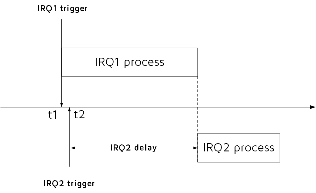
The feature 1 above determines that the MCU responds to interrupts on a first-come, first-served basis. When the first interrupt is not processed, a new interrupt is generated and cannot be responded to immediately and enters the waiting queue until the previous interrupts are processed. Therefore, when there are 2 or more interrupts, all interrupts cannot be responded in real time. The response delay of a particular interrupt depends on whether the MCU is processing other interrupts when this interrupt is triggered and how long it takes to process the other interrupts. As shown in the figure below, since IRQ1 is processing when IRQ2 is triggered, it must wait until IRQ1 is finished processing before responding. The worst case of IRQ 2 delay time is the maximum time of IRQ1 process.
In the BLE SDK, two system interrupts, system timer and RF, are used. If the user does not add new interrupts, there is no need to consider the timing of the two system interrupts; if the customer needs to add other interrupts (e.g. UART, PWM, etc.), the details to be considered are as follows.
(1) For the two system interrupts system timer and RF in the SDK, the maximum possible execution time is 200us. This means that the customer added interrupts may not be able to respond in real time, and the theoretical maximum possible delay time is 200us.
(2) The two system interrupts system timer and RF are for processing BLE tasks, due to the BLE timing is more strict, can not be delayed too long. Therefore, the processing time of the interrupts added by the customer should not be too long, and it is recommended to be within 50us. If the time is too long, there may be BLE timing synchronization errors, resulting in low efficiency of sending and receiving packets, high power consumption, BLE disconnection and other problems.
BLE Module
BLE SDK Software Architecture
Standard BLE SDK Architecture
Figure below shows standard BLE SDK software architecture compliant with BLE spec.
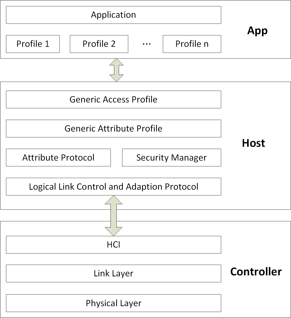
As shown above, BLE protocol stack includes Host and Controller.
-
As BLE bottom-layer protocol, the “Controller” contains Physical Layer (PHY) and Link Layer (LL). Host Controller Interface (HCI) is the sole communication interface for all data transfer between Controller and Host.
-
As BLE upper-layer protocol, the “Host” contains protocols including Logic Link Control and Adaption Protocol (L2CAP), Attribute Protocol (ATT), Security Manager Protocol (SMP), as well as Profiles including Generic Access Profile (GAP) and Generic Attribute Profile (GATT).
-
The “Application” (APP) layer contains user application codes and Profiles corresponding to various Services. User controls and accesses Host via “GAP”, while Host transfers data with Controller via “HCI”, as shown below.
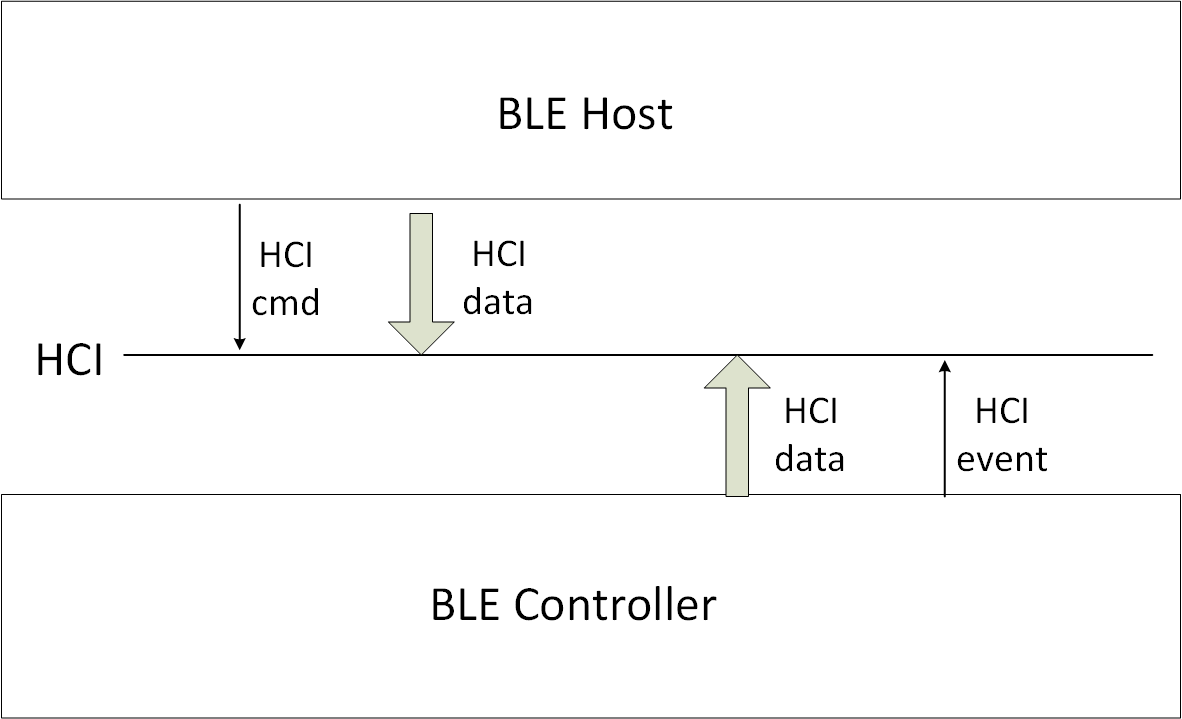
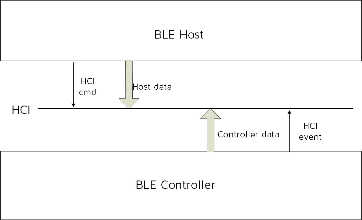
(1) BLE Host will use HCI cmd to operate and set Controller. Controller API corresponding to each HCI cmd will be introduced in this chapter.
(2) Controller will report various HCI events to Host via HCI.
(3) Host will send target data to Controller via HCI, while Controller will directly load data to Physical Layer for transfer.
(4) When Controller receives RF data in Physical Layer, it will first check whether the data belong to Link Layer or Host, and then process correspondingly: If the data belong to LL, the data will be processed directly; if the data belong to Host, the data will be sent to Host via HCI.
Telink BLE SDK Architecture
Telink BLE controller
Telink BLE SDK supports standard BLE controllers, including HCI, PHY (Physical Layer) and LL (Link layer).
B80 BLE Single Connection SDK includes three standard states of Link Layer (standby, advertising, connection), and the conneciton state only supports the Slave role. The Slave role in the B80 BLE Single Connection SDK is only a single connection, that is, the Link Layer can only maintain one connection, and multiple Slaves cannot exist at the same time.
The B80 hci in the SDK is a BLE slave controller, which needs to coordinate with another MCU running BLE Host to form a standard BLE Slave system, the architecture diagram is as follows.
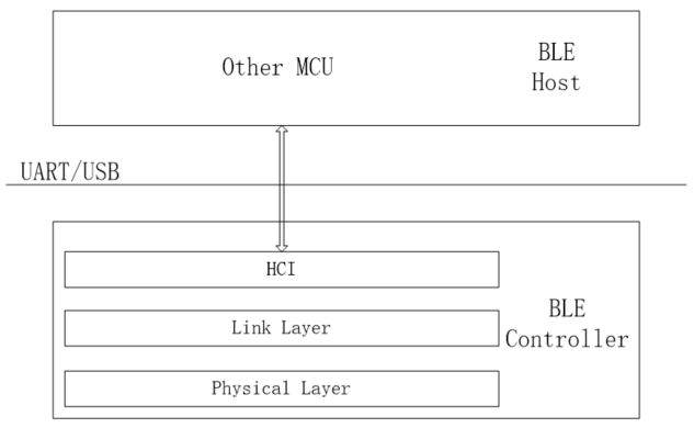
Telink BLE Slave
B80 BLE Single Connection SDK in BLE host and only supports the Slave part.
When user only needs to use standard BLE Slave, and Telink BLE SDK runs Host (Slave part) + standard Controller, the actual stack architecture will be simplified based on the standard architecture, so as to minimize system resource consumption of the whole SDK (including SRAM, running time, power consumption, and etc.). Following shows Telink BLE Slave architecture. In the SDK, B80 ble sample and B80 module are based on this architecture.
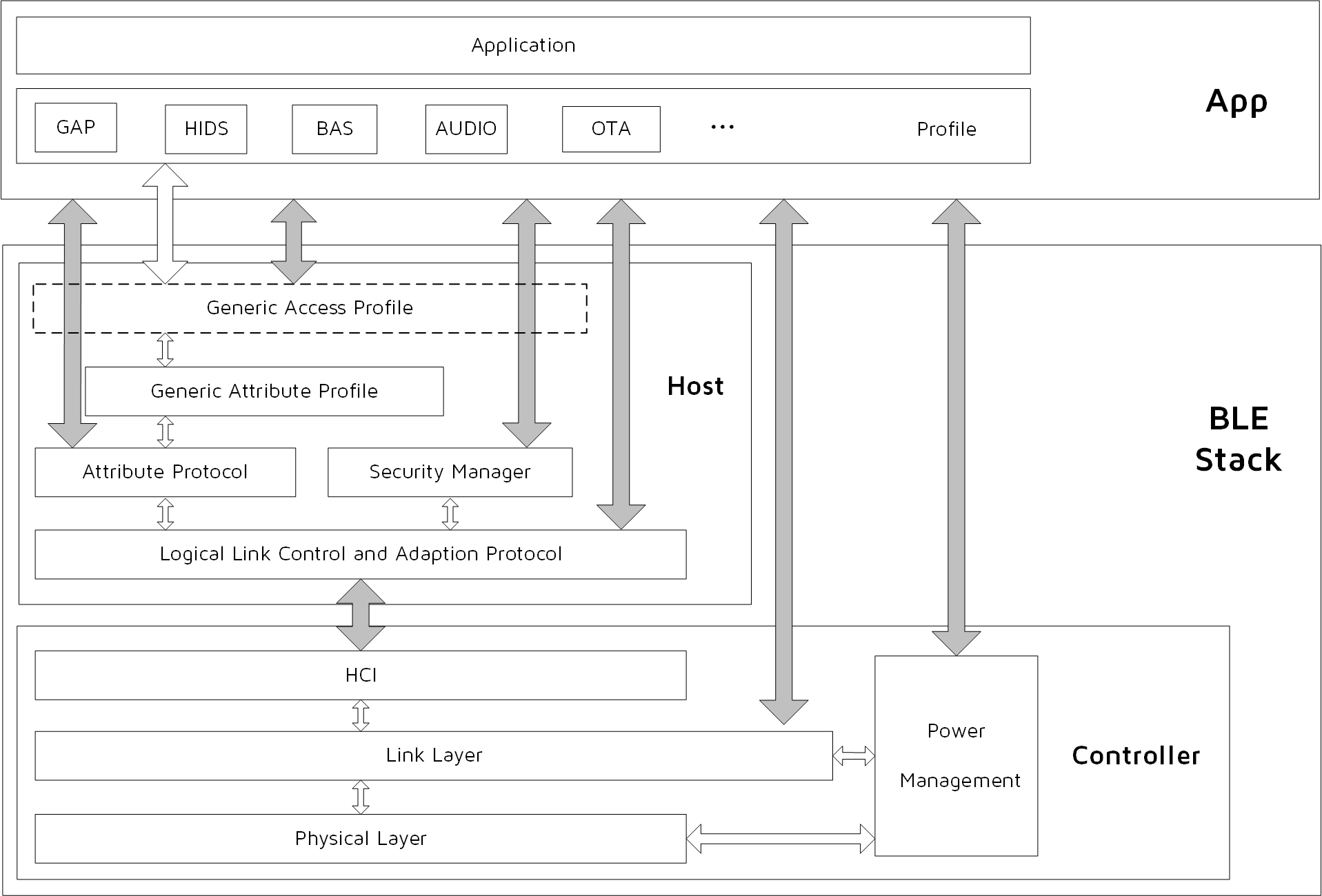
In figure above, solid arrows indicate data transfer controllable via user APIs, while hollow arrows indicate data transfer within the protocol stack not involved in user.
Controller can still communicate with Host (L2CAP layer) via HCI; however, the HCI is no longer the sole interface, and the APP layer can directly exchange data with Link Layer of the Controller. Power Management (PM) Module is embedded in the Link Layer, and the application layer can invoke related PM interfaces to set power management.
Considering efficiency, data transfer between the APP layer and the Host is not controlled via GAP; the ATT, SMP and L2CAP can directly communicate with the APP layer via corresponding interface. However, the event of the Host should be communicated with the APP layer via the GAP layer.
Generic Attribute Profile (GATT) is implemented in the Host layer based on Attribute Protocol. Various Profiles and Services can be defined in the APP layer based on GATT. Basic Profiles including HIDS, BAS and OTA are provided in demo code of this BLE SDK.
Following sections explain each layer of the BLE stack according to the structure above, as well as user APIs for each layer.
Physical Layer is totally controlled by Link Layer, since it does not involve the application layer, it will not be covered in this document.
Though HCI still implements part of data transfer between Host and Controller, it is basically implemented by the protocol stack of Host and Controller with little involvement of the APP layer. User only needs to register HCI data callback handling function in the L2CAP layer.
BLE Controller
BLE Controller Introduction
BLE Controller contains Physical Layer, Link Layer, HCI and Power Management.
Telink BLE SDK fully packs Physical Layer in the library (corresponding to c file of rf.h in driver file), and user does not need to learn about it. Power Management will be introduced in detail in section 4 Low Power Management (PM).
This section will focus on Link Layer, and also introduce HCI related interfaces to operate Link Layer and obtain data of Link Layer.
Link Layer State Machine
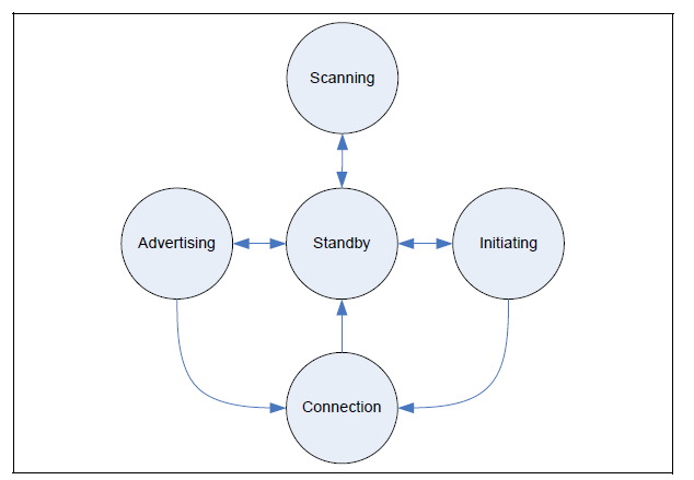
Figure below shows Link Layer state machine in BLE spec. Please refer to “Core_v4.2” (Vol 6/Part B/1.1 “LINK LAYER STATES”) for more information.
B80 BLE Single Connection SDK Link Layer state machine is shown as below.
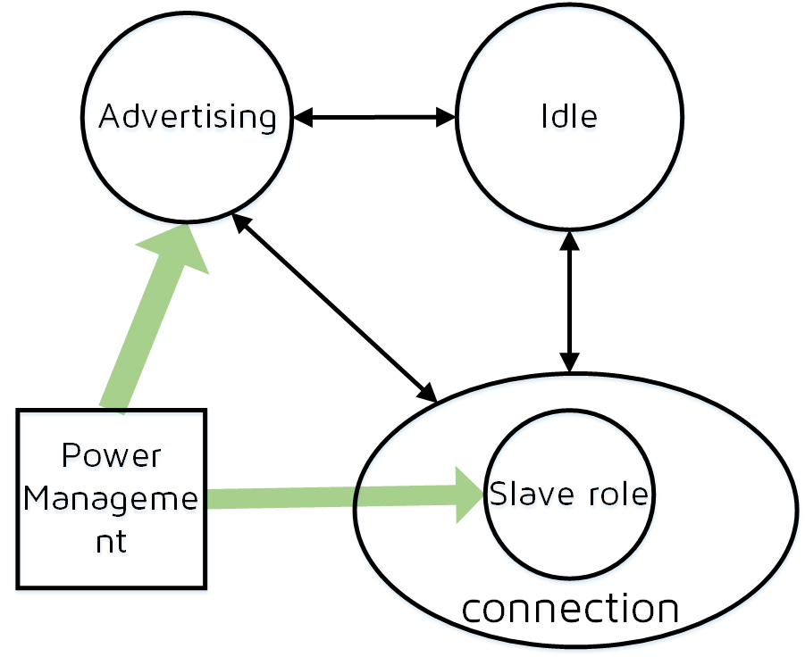
Since the B80 BLE Single Connection SDK only supports Slave Role, the state machine only has three basic states: Idle (Standby), Advertising, and Connection (Slave Role). Connection (Slave Role) will be referred to later as ConnSlaveRole.
The "Power Management" in figure above is not a state of LL, but a functional module which indicates the SDK only handles low power processing for Advertising and ConnSlaveRole. If the idle state requires low power consumption, the user can call the relevant API at the application layer to complete.
Based on the three states above, corresponding state machine names are defined in the “stack/ble/ll/ll.h”.
#define BLS_LINK_STATE_IDLE         0
#define BLS_LINK_STATE_ADV          BIT(0)
#define BLS_LINK_STATE_CONN         BIT(3)
Switch of Link Layer state machine is automatically implemented in BLE stack bottom layer. Therefore, user cannot modify state in APP layer, but can obtain current state by invoking the API below. The return value will be one of the three states.
u8 blc_ll_getCurrentState(void);
Link Layer State Machine Combined Application
(1) Link Layer State Machine Initialization
The state machine is flexible in design, and ach state is encapsulated as a module. By default, there is only the most basic Idle module, and users can add modules to build their own state machine combinations to implement different applications. For example, if the application only needs Advertising, then only the Advertising module needs to be added, and the remaining ConnSlaveRole modules are not configured. The purpose of this design is to save code size, and the relevant code of the state that does not need to be used will not be compiled in.
The MCU initialization is mandatory and the API is as follows.
void blc_ll_initBasicMCU (void);
The API below serves to add the basic Idle module. This API is also necessary for all BLE applications.
void blc_ll_initStandby_module (u8 *public_adr);
The initialization APIs of the corresponding modules of Advertising and ConnSlaveRole are as follows.
void        blc_ll_initAdvertising_module(void);
void        blc_ll_initSlaveRole_module(void);
The real parameter public_adr in the above API is a pointer to the BLE public mac address.
User uses the above APIs to combine the Link Layer state machine. Two common combinations and corresponding application scenarios are given below.
(2) Idle + Advertising

As shown above, only Idle and Advertising module are initialized, and it applies to applications which use basic advertising function to advertise product information in single direction, e.g. beacon.
Following is module initialization code of Link Layer state machine.
u8  mac_public[6] = {……};
blc_ll_initBasicMCU();
blc_ll_initStandby_module(mac_public);
blc_ll_initAdvertising_module();
State switch of Idle and Advertising is implemented via the “bls_ll_setAdvEnable”.
(3) Idle + Advertising + ConnSlaveRole
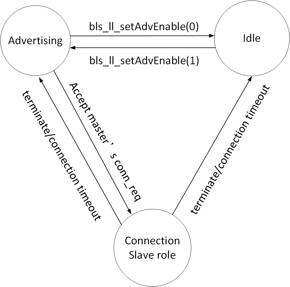
The figure above shows the Link Layer state machine combination for a basic BLE slave application. The 8208 hci/ 8208 ble sample/ 8208 module in the SDK are all based on this state machine combination.
The Link Layer state machine module is initialized with the following code.
u8  mac_public[6] = {……};
blc_ll_initBasicMCU();
blc_ll_initStandby_module(mac_public);
blc_ll_initAdvertising_module();
blc_ll_initSlaveRole_module();
State switch in this combination is shown as below:
a. After power on, the MCU enters Idle state. In Idle state, when adv is enabled, Link Layer switches to Advertising state; when adv is disabled, it will return to Idle state.
The API “bls_ll_setAdvEnable” serves to enable/disable Adv.

After power on, Link Layer is in Idle state by default. Typically it’s needed to enable Adv in the “user_init” so as to enter Advertising state.
b. When Link Layer is in Idle state, Physical Layer won’t take any RF operation including packet transmission and reception.
c. When Link Layer is in Advertising state, advertising packets are transmitted in adv channels. Master will send conneciton request if it receives adv packet. After Link Layer receives this connection request, it will respond, establish connection and enter ConnSlaveRole.
d. When Link Layer is in ConnSlaveRole, it will return to Idle State or Advertising state in any of the following cases:
-
Master sends “terminate” command to Slave and requests disconnection. Slave will exit ConnSlaveRole after it receives this command.
-
By sending “terminate” command to Master, Slave actively terminates the connection and exits ConnSlaveRole.
-
If Slave fails to receive any packet due to Slave RF Rx abnormity or Master Tx abnormity until BLE connection supervision timeout is triggered, Slave will exit ConnSlaveRole.
When ConnSlaveRole of Link layer exits this state, it switches to a different state depending on whether Adv is enabled or not: if Adv is enabled, Link Layer goes back to Advertising state; if Adv is Disable, Link Layer goes back to Idle state. Whether Adv is Enable or Disable depends on the value set by the user when bls_ll_setAdvEnable was last called by the application layer.
Link Layer Timing Sequence
In this section, Link Layer timing sequence in various states will be illustrated combining with irq_handler and main_loop of this BLE SDK.
_attribute_ram_code_ void irq_handler(void)
{
    ……
    blc_sdk_irq_handler ();
    ……
}

void main_loop (void)
{
///////////////////// BLE entry ////////////////////////////
    blc_sdk_main_loop();
////////////////////// UI entry ////////////////////////////
    ……
}
The "blc_sdk_main_loop" function at BLE entry serves to process data and events related to BLE protocol stack. UI entry is for user application code.
Idle State Timing Sequence
When Link Layer is in Idle state, no task is processed in Link Layer and Physical Layer; the "blc_sdk_main_loop" function doesn’t act and won’t generate any interrupt, i.e. the whole timing sequence of main_loop is occupied by UI entry.
Advertising State Timing Sequence

As shown in figure above, an Adv event is triggered by Link Layer during each adv interval. A typical Adv event with three active adv channels will send an advertising packet in channel 37, 38 and 39, respectively. After an adv packet is sent, Slave enters Rx state, and waits for response from Master:
-
If Slave receives a scan request from Master, it will send a scan response to Master.
-
If Slave receives a connect request from Master, it will establish BLE connection with Master and enter Connection state Slave Role.
Code of UI entry in main_loop is executed during UI task/suspend part in figure above. This duration can be used for UI task only, or MCU can enter sleep (suspend or deep sleep retention) for the redundant time to reduce power consumption.
In Advertising state, the "blc_sdk_main_loop" function does not need to process many tasks, and only some callback events related to Adv will be triggered, including BLT_EV_FLAG_ADV_DURATION_TIMEOUT、BLT_EV_FLAG_SCAN_RSP, BLT_EV_FLAG_CONNECT, etc.
Conn State Slave Role Timing Sequence

As shown in the above figure, each conn interval starts with a brx event, i.e. transfer process of BLE RF packets by Link Layer: PHY enters Rx state, and an ack packet will be sent to respond to each received data packet from Master. If there is more data, then continue to receive master packets and reply, this process is called brx event for short.
In this BLE SDK, each brx process consists of three phases according to the assignment of hardware and software.
(1) brx start phase
When Master is about to send packet, an interrupt is triggered by system tick irq to enter brx start phase. During this interrupt, MCU sets BLE state machine of PHY to enter brx state, hardware in bottom layer prepares for packet transfer, and then MCU exits from the interrupt irq.
(2) brx working phase
After brx start phase ends and MCU exits from irq, hardware in bottom layer enters Rx state first and waits for packet from Master. During the brx working phase, all packet reception and transmission are implemented automatically without involvement of software.
(3) brx post phase
After packet transfer is finished, the brx working phase is completed. System tick irq triggeres an interrupt to switch to the brx post phase. During this phase, protocol stack will process BLE data and timing sequence according to packet transfer in the brx working phase.
During the three phases, brx start and brx post are implemented in interrupt, while brx working phase does not need the involvement of software, and UI task can be executed normally (Note that during brx working phase, UI task can be executed in the time slots except RX, TX, and System Timer interrupt handler). During the brx working phase, MCU can’t enter sleep (suspend or deep sleep retention) since hardware needs to transfer packets.
Within each conn interval, the duration except for brx event can be used for UI task only, or MCU can enter sleep (suspend or deep sleep retention) for the redundant time to reduce power consumption.
In the ConnSlaveRole, the "blc_sdk_main_loop" needs to process the data received during the brx process. During the brx working phase, the data packet received from Master will be copied out during RX interrupt irq handler; these data won’t be processed immediately, but buffered in software RX fifo (corresponding to app_acl_rxfifo in code). The "blc_sdk_main_loop" function will check whether there are data in software RX fifo, and process the detected data packet correspondingly:
The processing of packets by blc_sdk_main_loop includes:
(1) Decryption of data packet
(2) Parsing of data packet
If the parsed data belongs to the control command sent by Master to Link Layer, this command will be executed immediately; if it’s the data sent by Master to Host layer, the data will be transferred to L2CAP layer via HCI interface.
Conn State Slave Role Timing Protect
ConnSlaveRole, each interval requires a send/receive packet event, which is the Brx Event above. In the B80 SDK, the Brx Event is triggered entirely by interrupts, so the MCU main system interrupt needs to be turned on all the time. If the user is in the Conn state for a long time and has to turn off the main system interrupt (e.g. to erase the Flash), the Brx Event will be stopped and the BLE timing will soon be messed up and eventually the connection will be disconnected.
In this situation, the SDK provides a protection mechanism that allows the user to disable the Brx Event without breaking the BLE timing, and the user needs to strictly follow this mechanism. The relevant API is as follows.
    int     bls_ll_requestConnBrxEventDisable(void);
    void    bls_ll_disableConnBrxEvent(void);
    void    bls_ll_restoreConnBrxEvent(void);
Call bls_ll_requestConnBrxEventDisable to request that the Brx Event be switched off.
(1) If the return value of this API is 0, it means that the user's application is not currently accepted, i.e. the Brx Event cannot be stopped at this time. During the Brx working phase at Conn state, the application cannot be accepted and the return value is 0. It must wait until the end of a full Brx Event to accept the application for the remaining UI task/suspend time.
(2) This API returns a non-zero value to indicate that the request can be accepted and the value returned is the time in ms allowed to stop the Brx Event. There are three cases for this event value:
a)If the current Link Layer is Alerting state or Idle state, the return value is 0xffff, that is, there is no Brx Event, and the user is allowed to turn off the system interrupt for any length of time.
b)If the current Conn state receives an update map or update connection parameter from the master and has not yet reached the update time point, the return time is the update time point minus the current time. In other words, the time to stop the Brx Event cannot exceed the update time, otherwise all the packets will not be received and the connection will be disconnected.
c)If the current state is Conn state and there is no update request from master, the return value is half of the current connection supervision timeout value. For example, if the current timeout is 1s, the return value is 500ms.
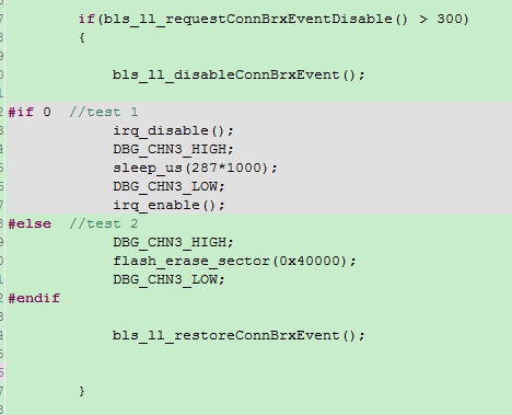
The user calls the above API to request to disable the Brx Event, and if the return value corresponds to enough time (ms) for the task to run itself, the task can be performed. Before the task is executed, API bls_ll_disableConnBrxEvent is called to disable the Brx Event. After the task is finished, API bls_ll_restoreConnBrxEvent is called to re-enable the Brx Event and repair the BLE timing.
The reference usage is as follows. Where the specific time is judged by the actual time of tested task.
Link Layer State Machine Extension
The above BLE Link Layer state machine and working timings introduce the most basic states, which can meet the basic application of BLE slave.
However, in view of the special applications that users may have, in the B80 BLE SDK, it adds the Conn state Slave role with the ability of advertising, which is described in more detail below.
Advertising in ConnSlaveRole
When the Link Layer is in ConnSlaveRole, the Advertising feature can be added.
The API to add Advertising feature:
ble_sts_t blc_ll_addAdvertisingInConnSlaveRole(void);
The API to remove Advertising feature:
ble_sts_t blc_ll_removeAdvertisingFromConnSLaveRole(void);
For the above two API, the return value of ble_sts_t type are both BLE_SUCCESS.
Combining the timing sequence of Advertising and ConnSlaveRole, when the Advertising feature is added to ConnSlaveRole, the timing sequence is as follows.

The current Link Layer is still in ConnSlaveRole (BLS_LINK_STATE_CONN) and executes an adv event immediately after the brx event in each Conn interval, and then leaves the rest of the time for the UI task or goes into sleep (suspend/ deepsleep retention) to save power.
For the usage of Advertising in ConnSlaveRole, please refer to the TEST_ADVERTISING_IN_CONN_SLAVE_ROLE in 8208_feature.
Link Layer TX fifo and RX fifo
All data from the application layer and the BLE Host eventually needs to be sent through the Link Layer of the Controller to complete the RF data. A BLE TX fifo is designed in the Link Layer, which can be used to cache the incoming data and to send the data after the brx/btx has started.
All data received from the peer device during Link Layer brx/btx is first stored in a BLE RX fifo before being uploaded to the BLE Host or application layer for processing.
Both BLE TX fifo and BLE RX fifo are defined in application layer app_buffer.c.
u8  app_acl_rxfifo[ACL_RX_FIFO_SIZE * ACL_RX_FIFO_NUM] = {0};
u8  app_acl_txfifo[ACL_TX_FIFO_SIZE * ACL_TX_FIFO_NUM] = {0};
Then configure into the underlying stack in app.c.
blc_ll_initAclConnTxFifo(app_acl_txfifo, ACL_TX_FIFO_SIZE, ACL_TX_FIFO_NUM);
blc_ll_initAclConnRxFifo(app_acl_rxfifo, ACL_RX_FIFO_SIZE, ACL_RX_FIFO_NUM);
The ACL_TX_FIFO_SIZE is 64 by default and the TX fifo size is 40 by default, and these two sizes are not allowed to be modified unless the data length extension is required.
Both TX fifo number and RX fifo number must be set to the power of 2, i.e. 2, 4, 8, 16, etc. Users can modify them slightly to suit their needs.
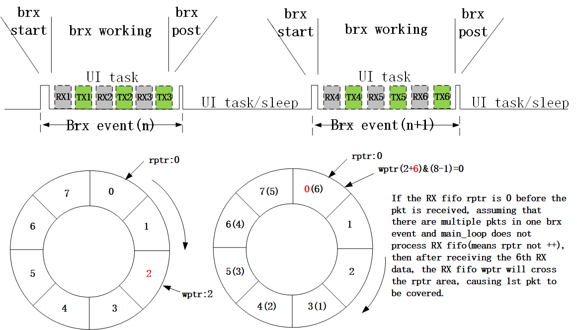
RX fifo number is 4 by default, which is a reasonable value and can ensure that the bottom layer of the Link Layer can buffer up to 4 packets. If the setting is too large, it will take up too much SRAM. If the setting is too small, there may be a risk of data overwriting: in the brx event, the Link Layer is likely to word under more data (MD) mode on an interval, and continue to receive multiple packets, if there are too few settings, it is likely that multiple packages (such as OTA) will appear in an interval, and the upper layer's response to these data is too long to process due to the long decryption time, then it is possible some data is overflowed.
Here is an example of RX overflow, we have the following assumptions:
(1) The number of RX fifo is 8;
(2) Before brx_event(n) is turned on, the read and write pointers of RX fifo are 0 and 2 respectively;
(3) In the brx_event(n) and brx_event(n+1) stages, the main_loop has task blockage, and the RX fifo is not taken in time;
(4) Both brx_event stages are multi-packet situations.
From the description in the “Conn state Slave role timing” section above, we know that the BLE data packets received in the brx_working stage will only be copied to the RX fifo (RX fifo write pointer++), and the RX fifo data is actually taken out for processing. In the main_loop stage (RX fifo read pointer++), we can see that the sixth data will cover the read pointer 0 area. It should be noted here that the UI task time slot in the brx working stage is the time except for interrupt processing such as RX, TX, and system timer.
Relative to the extreme case above with long task blockade duration due to one connection interval, the case below is more likely to occur: During one brx_event, since Master writes multiple packets (e.g. 7/8 packets) into Slave, Slave fails to process the received data in time. As shown below, the rptr (read pointer) is increased by two, but the wptr (write pointer) is also increased by eight, which thus causes data overflow.
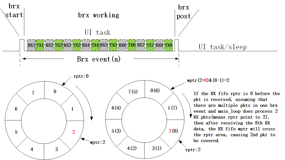
Once there is a data loss problem caused by overflow, for the encryption system, there will be a MIC failure disconnection problem. (For old SDK, as brx event Rx IRQ will fill data to Rx fifo but not do data overflow check, if main_loop is too slow to process RX fifo it will lead to overflow problem, so when using old SDK, user need to pay more attention to this risk, avoid master to send too much data on one connection interval, pay attention to user UI that the task processing time is as short as possible to avoid blocking problems.)
Rx overflow checks have now been added to the SDK. Check whether the current RX fifo write pointer and read pointer difference is greater than the number of Rx fifo in brx/btx event Rx IRQ. Once the Rx fifo is found to be full, the RF will not ACK the other party. BLE protocol Data retransmission will be ensured. In addition, the SDK also provides the Rx overflow callback function to notify users. This callback will be introduced in the chapter "Telink defined event" later in the document.
Similarly, if there may be more than 8 valid packets in an interval, the default 8 is not enough.
The TX fifo number is 16 by default, which is able to handle the larger data volume of the voice remote control function. Users can modify it to 8 if they do not use such a large fifo.
The TX fifo number is 8 by default. If the setting is too large (such as 16), it will take up too much Sram.
In the TX fifo, the SDK bottom layer stack needs to use 2, and the rest is used exclusively by the application layer; for a TX fifo of 16, the application layer can only use 14; for 8, the application layer can only use 6.
When sending data from the application layer (e.g. calling blc_gatt_pushHandleValueNotify), the user should first check how many TX fifo's are currently available in the Link Layer.
The following API is used to determine how many TX fifo's are currently occupied, not how many are left.
u8 blc_ll_getTxFifoNumber (void);
For example, if the TX fifo number defaults to 16, there are 14 users available, so the value returned by the API is available as long as it is less than 14: a return of 13 means there is 1 available, and a return of 0 means there are 14 available.
When using TX fifo, if the customer first looks at how many are left before deciding whether to push the data directly, a fifo should be left in place to prevent various boundary issues from occurring.
Controller Event
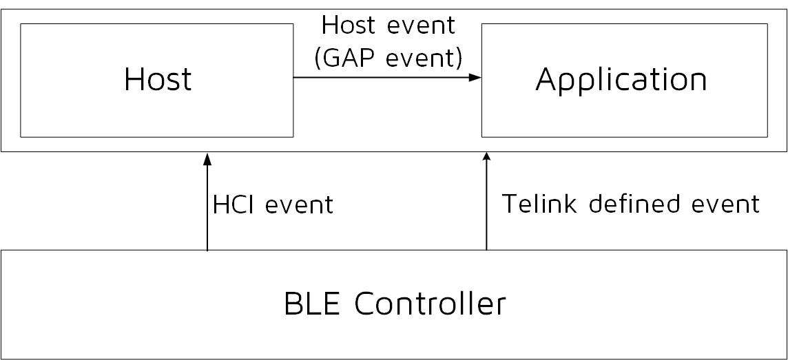
Considering user may need to record and process some key actions of BLE stack bottom layer in the APP layer, Telink BLE SDK provides three types of event: Standard HCI event defined by BLE Controller; Telink defined event; event-notification type GAP event (Host event) defined by BLE Host for stack flow interaction (see section GAP event).
As shown in the BLE SDK event architecture below: HCI event and Telink defined event are Controller event, while GAP event is BLE Host event.
Controller HCI Event
HCI event is designed according to BLE Spec standard, for BLE slave, HCI event and Telink defined event are available at the same time.
For BLE Slave, the two sets of events are basically independent of each other, and only two events are repeatedly defined: the connect and disconnect event of Link Layer, which will be described later.
User can select one set or use both as needed.
As shown in the “Host + Controller” architecture below, Controller HCI event indicates all events of Controller are reported to Host via HCI.
For definition of Controller HCI event, please refer to "Core_v4.2" (Vol 2/Part E/7.7 “Events”). “LE Meta Event” in 7.7.65 indicates HCI LE (low energy) Event, while the others are commom HCI events. As defined in Spec, Telink BLE SDK also divides Controller HCI event into two types: HCI Event and HCI LE event. Since Telink BLE SDK focuses on BLE, it supports most HCI LE events and only a few basic HCI events.
For the definition of macros and interfaces related to Controller HCI event, please refer to head files under “stack/ble/hci”.
To receive Controller HCI event in Host or APP layer, user should register callback function of Controller HCI event, and then enable mask of corresponding event.
Following are callback function prototype and register interface of Controller HCI event:
typedef int (*hci_event_handler_t) (u32 h, u8 *para, int n);
void  blc_hci_registerControllerEventHandler(hci_event_handler_t  handler);
In the callback function prototype, "u32 h" is a mark which will be frequently used in bottom-layer stack, and user only needs to know the following:
#define         HCI_FLAG_EVENT_TLK_MODULE           (1<<24)
#define         HCI_FLAG_EVENT_BT_STD               (1<<25)
The "HCI_FLAG_EVENT_TLK_MODULE" will be introduced in "Telink defined event", while "HCI_FLAG_EVENT _BT_STD" indicates current event is Controller HCI event.
In the callback function prototype, "para" and "n" indicate data and data length of event. The data is consistent with the definition in BLE spec.
HCI event
Telink BLE SDK supports a few HCI events. Following lists some events for user.
#define HCI_EVT_DISCONNECTION_COMPLETE                  0x05
#define HCI_EVT_ENCRYPTION_CHANGE                       0x08
#define HCI_EVT_READ_REMOTE_VER_INFO_COMPLETE           0x0C
#define HCI_EVT_ENCRYPTION_KEY_REFRESH                  0x30
#define HCI_EVT_LE_META                                 0x3E
(1) HCI_EVT_DISCONNECTION_COMPLETE
Please refer to “Core_v5.0” (Vol 2/Part E/7.7.5 “Disconnection Complete Event”). Total data length of this event is 7, and 1-byte “param len” is 4, as shown below. Please refer to BLE spec for data definition.

(2) HCI_EVT_ENCRYPTION_CHANGE and HCI_EVT_ENCRYPTION_KEY_REFRESH
Please refer to “Core_v5.0” (Vol 2/Part E/7.7.8 & 7.7.39). The two events are related to Controller encryption, and the processing is assembled in library.
(3) HCI_EVT_READ_REMOTE_VER_INFO_COMPLETE
Please refer to “Core_v5.0” (Vol 2/Part E/7.7.12). When Host uses the “HCI_CMD_READ_REMOTE_VER_INFO” command to exchange version information between Controller and BLE peer device, and version of peer device is received, this event will be reported to Host. Total data length of this event is 11, and 1-byte “param len” is 8, as shown below. Please refer to BLE spec for data definition.

(4) HCI_EVT_LE_META
It indicates current event is HCI LE event, and event type can be judged according to sub event code. Except for HCI_EVT_LE_META, other HCI events should use the API below to enable corresponding event mask.
ble_sts_t blc_hci_setEventMask_cmd(u32 evtMask);
Definition of event mask:
#define HCI_EVT_MASK_DISCONNECTION_COMPLETE                                 0x0000000010
#define HCI_EVT_MASK_ENCRYPTION_CHANGE                                      0x0000000080
#define HCI_EVT_MASK_READ_REMOTE_VERSION_INFORMATION_COMPLETE               0x0000000800
If the user does not set the HCI event mask via this API, the SDK will only turn on the mask corresponding to HCI_CMD_DISCONNECTION_COMPLETE by default, i.e. to ensure that the Controller disconnect event is reported.
HCI LE event
When event code in HCI event is “HCI_EVT_LE_META” to indicate HCI LE event, common sub-event code are shown as below:
#define HCI_SUB_EVT_LE_CONNECTION_COMPLETE                          0x01
#define HCI_SUB_EVT_LE_ADVERTISING_REPORT                           0x02
#define HCI_SUB_EVT_LE_CONNECTION_UPDATE_COMPLETE                   0x03
#define HCI_SUB_EVT_LE_CONNECTION_ESTABLISH                         0x20
(1) HCI_SUB_EVT_LE_CONNECTION_COMPLETE
Please refer to “Core_v5.0” (Vol 2/Part E/7.7.65.1 “LE Connection Complete Event”). When connection is established between Controller Link Layer and peer device, this event will be reported. Total data length of this event is 22, and 1-byte “param len” is 19, as shown below. Please refer to BLE spec for data definition.

(2) HCI_SUB_EVT_LE_ADVERTISING_REPORT
Please refer to “Core_v5.0” (Vol 2/Part E/7.7.65.2 “LE Advertising Report Event”). When Link Layer of Controller scans right adv packet, it will be reported to Host via the “HCI_SUB_EVT_LE_ADVERTISING_REPORT”. Data length of this event is not fixed and it depends on payload of adv packet, as shown below. Please refer to BLE spec for data definition.

Note: In Telink BLE SDK, each “LE Advertising Report Event” only reports an adv packet, i.e. “i” in figure above is 1.
(3) HCI_SUB_EVT_LE_CONNECTION_UPDATE_COMPLETE
Please refer to “Core_v5.0” (Vol 2/Part E/7.7.65.3 “LE Connection Update Complete Event”). When “connection update” in Controller takes effect, the “HCI_SUB_EVT_LE_CONNECTION_UPDATE_COMPLETE” will be reported to Host. Total data length of this event is 13, and 1-byte “param len” is 10, as shown below. Please refer to BLE spec for data definition.

“HCI LE event” needs the API below to enable mask.
ble_sts_t blc_hci_le_setEventMask_cmd(u32 evtMask);
Following lists some evtMask definitions. User can view the other events in the “hci_const.h”.
#define HCI_LE_EVT_MASK_CONNECTION_COMPLETE             0x00000001
#define HCI_LE_EVT_MASK_ADVERTISING_REPORT              0x00000002
#define HCI_LE_EVT_MASK_CONNECTION_UPDATE_COMPLETE      0x00000004
If HCI LE event mask is not set via this API, mask of all HCI LE events in the SDK are disabled by default.
Telink Defined Event
Besides standard Controller HCI event, the SDK also provides Telink defined event. Up to 20 Telink defined events are supported, which are defined by using macros in the “stack/ble/ll/ll.h”.
Current SDK version supports the following callback events. The “BLT_EV_FLAG_CONNECT / BLT_EV_FLAG_ TERMINATE” has the same function as the “HCI_SUB_EVT_LE_CONNECTION_COMPLETE” / “HCI_EVT_ DISCONNECTION_COMPLETE” in HCI event, but data definition of these events are different.
#define         BLT_EV_FLAG_ADV                     0
#define         BLT_EV_FLAG_ADV_DURATION_TIMEOUT    1
#define         BLT_EV_FLAG_SCAN_RSP                2
#define         BLT_EV_FLAG_CONNECT                 3
#define         BLT_EV_FLAG_TERMINATE               4
#define         BLT_EV_FLAG_LL_REJECT_IND           5
#define         BLT_EV_FLAG_RX_DATA_ABANDOM         6
#define         BLT_EV_FLAG_PHY_UPDATE              7
#define         BLT_EV_FLAG_DATA_LENGTH_EXCHANGE    8
#define         BLT_EV_FLAG_GPIO_EARLY_WAKEUP       9
#define         BLT_EV_FLAG_CHN_MAP_REQ             10
#define         BLT_EV_FLAG_CONN_PARA_REQ           11
#define         BLT_EV_FLAG_CHN_MAP_UPDATE          12
#define         BLT_EV_FLAG_CONN_PARA_UPDATE        13
#define         BLT_EV_FLAG_SUSPEND_ENTER           14
#define         BLT_EV_FLAG_SUSPEND_EXIT            15
Telink defined event is only triggered in BLE slave applications. There are two ways to implement callback of Telink defined event in BLE slave application.
(1) The first method, which is called “independent registration”, is to independently register callback function for each event.
Prototype of callback function is shown as below:
typedef void (*blt_event_callback_t)(u8 e, u8 *p, int n);
Where “e”: event number. “p”: It’s the pointer to the data transmitted from the bottom layer when callback function is executed, and it varies with the callback function. “n”: length of valid data pointed by pointer.
API to register callback function:
void bls_app_registerEventCallback (u8 e, blt_event_callback_t p);
Whether each event will respond depends on whether corresponding callback function is registered in APP layer.
(2) The second method, which is called “shared event entry”, is that all event callback functions share the same entry. Whether each event will respond depends on whether its event mask is enabled. This method uses the same API as HCI event to register event callback:
typedef int (*hci_event_handler_t) (u32 h, u8 *para, int n);
void  blc_hci_registerControllerEventHandler(hci_event_handler_t  handler);
Although registered callback function of HCI event is shared, they are different in implementation. In HCI event callback function:
h = HCI_FLAG_EVENT_BT_STD | hci_event_code;
While in Telink defined event “shared event entry”:
h = HCI_FLAG_EVENT_TLK_MODULE | e;
Where “e” is event number of Telink defined event.
Telink defined event “shared event entry” is similar to mask of HCI event; the API below serves to set the mask to determine whether each event will be responded.
ble_sts_t bls_hci_mod_setEventMask_cmd(u32 evtMask);
Relationship between evtMask and event number is:
evtMask = BIT(e);
The two methods for Telink defined event are exclusive to each other. The first method is recommended and is adopted by most demo code of the SDK; only "8208_ module" uses the "shared event entry" method.
For the use of Telink defined event, please refer to the demo code of project "8208_module" for 2 "shared event entry".
The following takes the connect and terminate event callbacks as examples to describe the code implementation methods of these two methods.
(1) The first method: “independent registration”
void    task_connect (u8 e, u8 *p, int n)
{
        // add connect callback code here
}

void    task_terminate (u8 e, u8 *p, int n)
{
        // add terminate callback code here
}
bls_app_registerEventCallback (BLT_EV_FLAG_CONNECT, &task_connect);
bls_app_registerEventCallback (BLT_EV_FLAG_TERMINATE, &task_terminate);
(2) The second method: “shared event entry”
int event_handler(u32 h, u8 *para, int n)
{
        if( (h&HCI_FLAG_EVENT_TLK_MODULE)!= 0 ) //module event
        {
            switch(event)
            {
                case BLT_EV_FLAG_CONNECT:
                {
                    // add connect callback code here
                }
                break;
                case BLT_EV_FLAG_TERMINATE:
                {
                    // add terminate callback code here
                }
            break;
                default:
            break;
            }
        }
}
blc_hci_registerControllerEventHandler(event_handler);
bls_hci_mod_setEventMask_cmd( BIT(BLT_EV_FLAG_CONNECT) | BIT(BLT_EV_FLAG_TERMINATE) );
Following will introduce details about all events, event trigger condition and parameters of corresponding callback function for Controller.
(1) BLT_EV_FLAG_ADV
This event is not used in current SDK.
(2) BLT_EV_FLAG_ADV_DURATION_TIMEOUT
Event trigger condition: If the API “bls_ll_setAdvDuration” is invoked to set advertising duration, a timer will be started in BLE stack bottom layer. When the timer reaches the specified duration, advertising is stopped, and this event is triggered. In the callback function of this event, user can modify adv event type, re-enable advertising, re-configure advertising duration, and etc.
Pointer “p”: null pointer.
Data length “n”: 0.
Note: This event won’t be triggered in “advertising in ConnSlaveRole” which is an extended state of Link Layer.
(3) BLT_EV_FLAG_SCAN_RSP
Event trigger condition: When Slave is in advertising state, this event will be triggered if Slave responds with scan response to the scan request from Master.
Pointer “p”: null pointer.
Data length “n”: 0.
(4) BLT_EV_FLAG_CONNECT
Event trigger condition: When Link Layer is in advertising state, this event will be triggered if it responds to connect reqeust from Master and enters Conn state Slave role.
Data length “n”: 34.
Pointer “p”: p points to one 34-byte RAM area, corresponding to the “connect request PDU” below.

(5) BLT_EV_FLAG_TERMINATE
Event trigger condition: This event will be triggered when Link Layer state machine exits from Conn state Slave role in any of the three specific cases.
Pointer “p”: p points to an u8-type variable “terminate_reason”. This variable indicates the reason for disconnection of Link Layer.
Data length “n”: 1.
Three cases to exit Conn state Slave role and corresponding reasons are listed as below:
a) If Slave fails to receive packet from Master for a duration due to RF communication problem (e.g. bad RF or Master is powered off), and “connection supervision timeout” expires, this event will be triggered to terminate connection and return to None Conn state. The terminate reason is HCI_ERR_CONN_TIMEOUT (0x08).
b) If Master sends “terminate” command to actively terminate connection, after Slave responds to the command with an ack, this event will be triggered to terminate connection and return to None Conn state. The terminate reason is the Error Code in the “LL_TERMINATE_IND” control packet received in Slave Link Layer. The Error Code is determined by Master. Common Error Codes include HCI_ERR_REMOTE_USER_TERM_CONN (0x13), HCI_ERR_CONN_TERM_MIC_FAILURE (0x3D), and etc.
c) If Slave invokes the API “bls_ll_terminateConnection(u8 reason)” to actively terminate connection, this event will be triggered. The terminate reason is the actual parameter “reason” of this API.
(6) BLT_EV_FLAG_LL_REJECT_IND
Event trigger condition: When Master sends a “LL_ENC_REQ” (encryption request) in the Link Layer and it’s declared to use the pre-allocated LTK, if Slave fails to find corresponding LTK and responds with a “LL_REJECT_IND” (or “LL_REJECT_EXT_IND”), this event will be triggered.
Pointer “p”: p points to the response command (LL_REJECT_IND or LL_REJECT_EXT_IND).
Data length “n”: 1.
For more information, please refer to “Core_v5.0” Vol 6/Part B/2.4.2.
(7) BLT_EV_FLAG_RX_DATA_ABANDOM
Event trigger condition: This event will be triggered when BLE RX fifo overflows (see section Link Layer TX fifo and RX fifo), or the number of More Data received in an interval exceeds the preset threshold (Note: User needs to invoke the API “blc_ll_init_max_md_nums” with non-zero parameter, so that SDK bottom layer will check the number of More Data.)
Pointer “p”: null pointer.
Data length “n”: 0.
(8) BLT_EV_FLAG_PHY_UPDATE
Event trigger condition: This event will be triggered after the update succeeds or fails when the slave or master proactively initiates LL_PHY_REQ; Or when the slave or master passively receives LL_PHY_REQ and meanwhile PHY is updated successfully, this event will be triggered.
Data length “n”: 1.
Pointer “p”: p points to an u8-type variable indicating the current connection of PHY mode.
typedef enum {
    BLE_PHY_1M          = 0x01,
    BLE_PHY_2M          = 0x02,
} le_phy_type_t;
(9) BLT_EV_FLAG_DATA_LENGTH_EXCHANGE
Event trigger condition: This event will be triggered when Slave and Master exchange max data length of Link Layer, i.e. one side sends “ll_length_req”, while the peer responds with “ll_length_rsp”. If Slave actively sends “ll_length_req”, this event won’t be triggered until “ll_length_rsp” is received. If Master initiates “ll_length_req”, this event will be triggered immediately after Slave responds with “ll_length_rsp”.
Data length “n”: 12.
Pointer “p”: p points to data of a memory area, corresponding to the beginning six u16-type variables in the structure below.
typedef struct {
    u16     connEffectiveMaxRxOctets;
    u16     connEffectiveMaxTxOctets;
    u16     connMaxRxOctets;
    u16     connMaxTxOctets;
    u16     connRemoteMaxRxOctets;
    u16     connRemoteMaxTxOctets;
            ……
}ll_data_extension_t;
The “connEffectiveMaxRxOctets” and “connEffectiveMaxTxOctets” are max RX and TX data length finally allowed in current connection; “connMaxRxOctets” and “connMaxTxOctets” are max RX and TX data length of the device; “connRemoteMaxRxOctets” and “connRemoteMaxTxOctets” are max RX and TX data length of peer device.
connEffectiveMaxRxOctets = min(supportedMaxRxOctets,connRemoteMaxTxOctets);
connEffectiveMaxTxOctets = min(supportedMaxTxOctets, connRemoteMaxRxOctets);
(10) BLT_EV_FLAG_GPIO_EARLY_WAKEUP
Event trigger condition: Slave will calculate wakeup time before it enters sleep (suspend or deepsleep retention), so that it can wake up when the wakeup time is due (It’s realized via timer in sleep). Since user tasks won’t be processed until wakeup from sleep, long sleep time may bring problem for real-time demanding applications. Take keyboard scanning as an example: If user presses keys fast, to avoid key press loss and process debouncing, it’s recommended to set the scan interval as 10~20ms; longer sleep time (e.g. 400ms or 1s, which may be reached when latency is enabled) will lead to key press loss. So it’s needed to judge current sleep time before MCU enters sleep; if it’s too long, the wakeup method of user key press should be enabled, so that MCU can wake up from sleep (suspend or deepsleep retention) in advance (i.e. before timer timeout) if any key press is detected. This will be introduced in details in following PM module section.
The event “BLT_EV_FLAG_GPIO_EARLY_WAKEUP” will be triggered if MCU is woke up from sleep (suspend or deepsleep) by GPIO in advance before wakeup timer expires.
Data length "n": 1.
Pointer "p": p points to an u8-type variable “wakeup_status”. This variable indicates valid wakeup source status for current suspend. Following types of wakeup status are defined in the "drivers/lib/include/pm.h":
enum {
     WAKEUP_STATUS_PAD              = BIT(0),
     WAKEUP_STATUS_CORE             = BIT(1),
     WAKEUP_STATUS_TIMER            = BIT(2),

     STATUS_GPIO_ERR_NO_ENTER_PM    = BIT(7),
     STATUS_ENTER_SUSPEND           = BIT(30),
};
For parameter definition above, please refer to “Low Power Management” section.
(11) BLT_EV_FLAG_CHN_MAP_REQ
Event trigger condition: When Slave is in Conn state, if Master needs to update current connection channel list, it will send a “LL_CHANNEL_MAP_REQ” command to Slave; this event will be triggered after Slave receives this request from Master and has not processed the request yet.
Data length “n”: 5.
Pointer “p”: p points to the starting address of the following channel list array.
unsigned char type bltc.conn_chn_map[5], Note: When the callback function is executed, p points to the old channel map before update.
Five bytes are used in the “conn_chn_map” to indicate current channel list by mapping. Each bit indicates a channel:
conn_chn_map[0] bit0-bit7 indicate channel0~channel7, respectively.
conn_chn_map[1] bit0-bit7 indicate channel8~channel15, respectively.
conn_chn_map[2] bit0-bit7 indicate channel16~channel23, respectively.
conn_chn_map[3] bit0-bit7 indicate channel24~channel31, respectively.
conn_chn_map[4] bit0-bit4 indicate channel32~channel36, respectively.
(12) BLT_EV_FLAG_CHN_MAP_UPDATE
Event trigger condition: When Slave is in connection state, this event will be triggered if Slave has updated channel map after it receives the “LL_CHANNEL_MAP_REQ” command from Master.
Pointer “p”: p points to the starting address of the new channel map conn_chn_map[5] after update.
Data length “n”: 5.
(13) BLT_EV_FLAG_CONN_PARA_REQ
Event trigger condition: When Slave is in connection state (Conn state Slave role), if Master needs to update current connection parameters, it will send a “LL_CONNECTION_UPDATE_REQ” command to Slave; this event will be triggered after Slave receives this request from Master and has not processed the request yet.
Data length “n”: 11.
Pointer “p”: p points to the 11-byte PDU of the LL_CONNECTION_UPDATE_REQ.

(14) BLT_EV_FLAG_CONN_PARA_UPDATE
Event trigger condition: When Slave is in connection state, this event will be triggered if Slave has updated connection parameters after it receives the “LL_CONNECTION_UPDATE_REQ” from Master.
Data length “n”: 6.
Pointer “p”: p points to the new connection parameters after update, as shown below.
p[0] | p[1]<<8: new connection interval in unit of 1.25ms.
p[2] | p[3]<<8: new connection latency.
p[4] | p[5]<<8: new connection timeout in unit of 10ms.
(15) BLT_EV_FLAG_SUSPEND_ENETR
Event trigger condition: When Slave executes the function “blc_sdk_main_loop”, this event will be triggered before Slave enters suspend.
Pointer “p”: Null pointer.
Data length “n”: 0.
(16) BLT_EV_FLAG_SUSPEND_EXIT
Event trigger condition: When Slave executes the function “blc_sdk_main_loop”, this event will be triggered after Slave is woke up from suspend.
Pointer “p”: Null pointer.
Data length “n”: 0.
Note:
This callback is executed after SDK bottom layer executes “cpu_sleep_wakeup” and Slave is woke up, and this event will be triggered no matter whether the actual wakeup source is gpio or timer. If the event “BLT_EV_FLAG_GPIO_EARLY_WAKEUP” occurs at the same time, for the sequence to execute the two events, please refer to pseudo code in “Power Management – PM Working Mechanism”.
Data Length Extension
BLE Spec core_4.2 and above supports Data Length Extension (DLE).
Link Layer in this BLE SDK supports data length extension to max rf_len of 251 bytes per BLE Spec.
Please refer to “Core_v5.0” (Vol 6/Part B/2.4.2.21 “LL_LENGTH_REQ and LL_LENGTH_RSP”).
Following steps explains how to use data length extension.
Step 1: Configure suitable TX & RX fifo size
To receive and transmit long packet, bigger Tx & Rx fifo size is required and thus ocupies large SRAM space. So be cautious when setting fifo size to avoid waste of SRAM or overflow of stack.
Tx fifo size should be increasd to transmit long packet. TX fifo size is at least 12 larger than TX rf_len, and must be aligned by 4 bytes. Modify ACL_CONN_MAX_TX_OCTETS directly in app_buffer.h, and the alignment will be automatically handled in the code.
#define ACL_CONN_MAX_TX_OCTETS 27
Rx fifo size should be increasd to receive long packet. Rx fifo size is at least 24 larger than Rx rf_len, and must be aligned by 16 bytes. Modify ACL_CONN_MAX_RX_OCTETS directly in app_buffer.h, and the alignment will be automatically handled in the code.
#define ACL_CONN_MAX_TX_OCTETS 27
Step 2: Set proper MTU size
MTU, the maximum transmission unit, is used to set the size of the payload in a single packet of the L2CAP layer in BLE. THe att.h provides the interface function ble_sts_t blc_att_setRxMtuSize(u16 mtu_size); during the initialization of the BLE stack, users can directly use this function to pass the parameter to set the MTU. However, the MTU size effect is negotiated in the MTU exchange process, MTU size effect = min(MTU_A, MTU_B), MTU_A is the MTU size supported by device A, MTU_B is the MTU size supported by device B; in addition, only MTU size greater than the DLE length can make full use of the DLE to increase the link layer data throughput rate.
For the implementation of MTU size exchange, please refer to the detailed description in the "ATT and GATT" section of this document, or refer to the DLE demo in 8208_feature.
#define MTU_SIZE_SETTING                    247
blc_att_setRxMtuSize(MTU_SIZE_SETTING);
Step 3: data length exchange
Before transfer of long packets, please make sure the “data length exchange” flow has already been completed in BLE connection. Data length exchange is an interactive process in Link Layer by LL_LENGTH_REQ and LL_LENGTH_RSP. Either master or slave can initiate the process by sending LL_LENGTH_REQ, while the peer responds with LL_LENGTH_RSP. Through this interaction, master and slave obtain the max Tx and Rx packet size from each other, and adopt the minimum of the two as the max Tx and Rx packet size in current connection.
No matter which side initiates LL_LENGTH_REQ, at the end of data length exchange process, the SDK will generate “BLT_EV_FLAG_DATA_LENGTH_EXCHANGE” event callback assuming this callback has been registered. User can refer to “Telink defined event” section to understand the parameters of this event callback function.
The final max Tx and Rx packet size can be obtained from the “BLT_EV_FLAG_DATA_LENGTH_EXCHANGE” event callback function.
When 8207 acts as slave device in actual applications, master may or may not initiate LL_LENGTH_REQ. If master does not initiate it, slave should initiate LL_LENGTH_REQ by the following API in the SDK:
ble_sts_t blc_ll_exchangeDataLength (u8 opcode, u16 maxTxOct);
In this API, “opcode” is “LL_LENGTH_REQ”, and “maxTxOct” is the max Tx packet size supported by current device. For example, if max Tx packet size is 200bytes, the setting below applies:
blc_ll_exchangeDataLength(LL_LENGTH_REQ , 200);
Since the slave device does not know whether the master will initiate LL_LENGTH_REQ, we recommend a method for your reference: register the BLT_EV_FLAG_DATA_LENGTH_EXCHANGE event callback, turn on a software timer to start timing when the connection is established (e.g. 2S), if this callback has not been triggered after 2s, it means that master has not initiated LL_LENGTH_REQ, at this time slave calls API blc_ll_exchangeDataLength to initiate LL_LENGTH_REQ.
Step 4: MTU size exchange
In addition to data length exchange, MTU size exchange flow should also be executed to ensure large MTU size takes effect, so that the peer can process long packet in BLE L2CAP layer. MTU size should be equal or larger than max packet size of Tx & Rx. Please refer to “ATT and GATT” section or the demo of the 8208_feature for the implementation of MTU size exchange.
Step 5: Transmission/Reception of long packet
Please refer to “ATT and GATT” section for illustration of Handle Value Notification, Handle Value Indication, Write request and Write Command.
Transmission and reception of long packet can start after correct completion of the three steps above.
The APIs corresponding to “Handle Value Notification” and “Handle Value Indication” can be invoked in ATT layer to transmit long packet. As shown below, fill in the address and length of data to be sent to the parameters “*p” and “len”, respectively:
ble_sts_t   blc_gatt_pushHandleValueNotify(u16 connHandle, u16 attHandle, u8 *p, int len);
ble_sts_t   blc_gatt_pushHandleValueIndicate(u16 connHandle, u16 attHandle, u8 *p, int len);
To receive long packet, it’s only needed to use callback function “w” corresponding to “Write Request” and “Write Command”.In the callback function, reference the data pointed to by the form reference pointer.
Controller API
Controller API Introduction
In standard BLE stack architecture of section 3.1.1, APP layer cannot directly communicate with Link Layer of Controller, i.e. data of APP layer must be first transferred to Host, and then Host can transfer control command to Link Layer via HCI. All control commands from Host to LL via HCI follow the definition in BLE spec “Core_v5.0”, please refer to “Core_v5.0” (Vol 2/Part E/ Host Controller Interface Functional Specification) for more information.
Telink BLE SDK based on standard BLE architecture can serve as a Controller and work together with Host system. Therefore, all APIs to operate Link Layer strictly follow the data format of Host commands in the spec.
Although the architecture in the figure above is used in Telink BLE SDK, during which APP layer can directly operate Link Layer, it still use the standard APIs of HCI part.
In BLE spec, all HCI commands to operate Controller have corresponding “HCI command complete event” or “HCI command status event” in response to Host layer. However, in Telink BLE SDK, it is handled case by case.
(1) For 8208_hci class applications, Telink IC only acts as a BLE controller and needs to work with other MCU's running BLE hosts, a corresponding HCI command complete event or HCI command status event will be generated for each HCI command.
(2) For 8208_sample application, both BLE Host and Controller are running on Telink IC, when Host calls interface to send HCI command to Controller, all of them are received correctly by Controller and there is no loss, so the Controller no longer replies to the HCI command complete event or HCI command status event when processing the HCI command.
The Controller API is declared in the header files in the stack/ble/ll and stack/ble/hci directories, where the ll directory is divided into ll.h, ll_adv.h, ll_slave.h, ll_pm.h, the user can look for Link Layer functions, for example, the APIs for functions related to advising should be declared in ll_adv.h.
API Return Type ble_sts_t
An enum type “ble_sts_t” defined in the “stack/ble/ble_common.h” is used as return value type for most APIs in the SDK. When API invoking with right parameter setting is accepted by the protocol stack, it will return “0” to indicate BLE_SUCCESS; if any non-zero value is returned, it indicates a unique error type. All possible return values and corresponding error reason will be listed in the subsections below for each API.
The “ble_sts_t” applies to both APIs in Link Layer and some APIs in Host layer.
BLE MAC address initialization
In this document, “BLE MAC address” includes both “public address” and “random static address”.
In this BLE SDK, the API below serves to obtain public address and random static address:
void blc_initMacAddress(int flash_addr, u8 *mac_public, u8 *mac_random_static);
The “flash_addr” is the flash address to store MAC address. As explained earlier, this address in 8208 512K flash is 0x76000. If random static address is not needed, set “mac_random_static” as “NULL”.
After the BLE public MAC address has been successfully obtained, the API for Link Layer initialization is called and the MAC address is passed into the BLE protocol stack.
blc_ll_initStandby_module(mac_public);
Link Layer state machine initialization
In conjunction with the previous detailed description of the Link Layer state machine, the following APIs are used to configure the initialisation of the individual modules when building the BLE state machine.
void        blc_ll_initBasicMCU (void)
void        blc_ll_initStandby_module (u8 *public_adr);
void        blc_ll_initAdvertising_module(void);
void        blc_ll_initSlaveRole_module(void);
bls_ll_setAdvData
Please refer to “Core_v5.0” (Vol 2/Part E/ 7.8.7 “LE Set Advertising Data Command”).

As shown above, an Adv packet in BLE stack contains 2-byte header, and Payload (PDU). The maximum length of Payload is 31 bytes.
The API below serves to set PDU data of adv packet:
ble_sts_t bls_ll_setAdvData(u8 *data, u8 len);
The “data” pointer points to the starting address of the PDU, while the “len” indicates data length.
The table below lists possible results for the return type “ble_sts_t”.
| ble_sts_t | Value | ERR Reason |
|---|---|---|
| BLE_SUCCESS | 0 | Success |
| HCI_ERR_INVALID_HCI_ CMD_PARAMS | 0x12 | Len exceeds the maximum length 31 |
This API can be invoked during initialization to set adv data, or invoked in main_loop to modify adv data when firmware is running.
In the "feature_backup" project of this BLE SDK, Adv PDU definition is shown as below. Please refer to “Data Type Specifcation” in BLE Spec “CSS v6” (Core Specification Supplement v6.0) for introduction to various fields.
const u8    tbl_advData[] = {
     8,  DT_COMPLETE_LOCAL_NAME,                'f','e','a','t','u','r','e',
     2,  DT_FLAGS,                              0x05,
     3,  DT_APPEARANCE,                         0x80, 0x01,
     5,  DT_INCOMPLT_LIST_16BIT_SERVICE_UUID,   0x12, 0x18, 0x0F, 0x18,
};
As shown in the adv data above, the adv device name is set as "feature".
bls_ll_setScanRspData
Please refer to “Core_v5.0” (Vol 2/Part E/ 7.8.8 “LE Set Scan response Data Command”).
The API below serves to set PDU data of scan response packet.
ble_sts_t bls_ll_setScanRspData(u8 *data, u8 len);
The "data" pointer points to the starting address of the PDU, while the “len” indicates data length.
The table below lists possible results for the return type "ble_sts_t".
| ble_sts_t | Value | ERR Reason |
|---|---|---|
| BLE_SUCCESS | 0 | Success |
| HCI_ERR_INVALID_HCI_ CMD_PARAMS | 0x12 | Len exceeds the maximum length 31 |
The user can call this API to set the Scan response data during initialization, or call this API in the main_loop at any time while the program is running to modify the Scan response data. The scan response data defined in the 8208_ble_sample project in the BLE SDK is as follows, and the scan device name is "eSample". For the meaning of each field, please refer to the specific description of Data Type Specifcation in the document BLE Spec "CSS v6" (Core Specification Supplement v6.0).
const u8    tbl_scanRsp [] = {
     8,  DT_COMPLETE_LOCAL_NAME,        'e', 'S', 'a', 'm', 'p', 'l', 'e',
};
The device name is set in the advertising data and scan response data above and is not the same. Then when scanning a Bluetooth device on a mobile phone or IOS system, the device name may be different:
(1) Some devices only watch broadcast packets, then the displayed device name is "feature";
(2) After seeing the broadcast, some devices send scan request and read back the scan response, then the displayed device name may be "eSample".
The user can also write the same device name in these two packages, and two different names will not be displayed when scanned.
In fact, after the device is connected by the master, when the master reads the Attribute Table of the device, it will obtain the gap device name of the device. After connecting to the device, it may also display the device name according to the settings there.
bls_ll_setAdvParam
Please refer to “Core_v5.0” (Vol 2/Part E/ 7.8.5 “LE Set Advertising Parameters Command”).

The figure above shows Advertising Event (Adv Event in brief) in BLE stack. It indicates during each T_advEvent, Slave implements one advertising process, and sends one packet in three advertising channels (channel 37, 38 and 39) respectively.
The API below serves to set parameters related to Adv Event.
ble_sts_t bls_ll_setAdvParam( u16 intervalMin, u16 intervalMax, adv_type_t advType, own_addr_type_t ownAddrType, u8 peerAddrType, u8 *peerAddr, adv_chn_map_t adv_channelMap, adv_fp_type_t advFilterPolicy);
(1) intervalMin & intervalMax
The two parameters serve to set the range of advertising interval in integer multiples of 0.625ms. The valid range is from 20ms to 10.24s, and intervalMin should not exceed intervalMax.
As required by BLE spec, it’s not recommended to set adv interval as fixed value; in Telink BLE SDK, the eventual adv interval is random variable within the range of intervalMin ~ intervalMax. If intervalMin and intervalMax are set as same value, adv interval will be fixed as the intervalMin.
Adv packet type has limits to the setting of intervalMin and intervalMax. Please refer to “Core 5.0” (Vol 6/Part B/ 4.4.2.2 “Advertising Events”) for details.
(2) advType
AS per BLE spec, the following four basic advertising event types are supported.
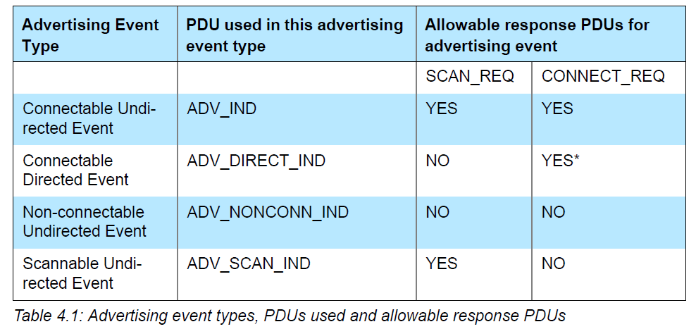
In the “Allowable response PDUs for advertising event” column, “YES” and “NO” indicate whether corresponding adv event type can respond to “Scan request” and “Connect Request” from other device. For example, “Connectable Undirected Event” can respond to both “Scan request” and “Connect Request”, while “Non-connectable Undireted Event” will respond to neither “Scan request” nor “Connect Request”.
For “Connectable Directed Event”, “YES” marked with an asterisk indicates the matched “Connect Request” received won’t be filtered by whitelist and this event will surely respond to it. Other “YES” not marked with asterisk indicate corresponding request can be responded depending on the setting of whitelist filter.
The “Connectable Directed Event” supports two sub-types including “Low Duty Cycle Directed Advertising” and “High Duty Cycle Directed Advertising”. Therefore, five types of adv events are supported in all, as defined below.
/* Advertisement Type */
typedef enum{
  ADV_TYPE_CONNECTABLE_UNDIRECTED             = 0x00,  // ADV_IND
  ADV_TYPE_CONNECTABLE_DIRECTED_HIGH_DUTY     = 0x01,  // ADV_INDIRECT_IND (high duty cycle)
  ADV_TYPE_SCANNABLE_UNDIRECTED               = 0x02 , // ADV_SCAN_IND
  ADV_TYPE_NONCONNECTABLE_UNDIRECTED          = 0x03 , // ADV_NONCONN_IND
  ADV_TYPE_CONNECTABLE_DIRECTED_LOW_DUTY      = 0x04,  // ADV_INDIRECT_IND (low duty cycle)
}adv_type_t;
By default, the most common adv event type is “ADV_TYPE_CONNECTABLE_UNDIRECTED”.
(3) ownAddrType
There are four optional values for “ownAddrType” to specify adv address type.
/* Own Address Type */
typedef enum{
    OWN_ADDRESS_PUBLIC = 0,
    OWN_ADDRESS_RANDOM = 1,
    OWN_ADDRESS_RESOLVE_PRIVATE_PUBLIC = 2,
    OWN_ADDRESS_RESOLVE_PRIVATE_RANDOM = 3,
}own_addr_type_t;
First two parameters are explained herein.
The “OWN_ADDRESS_PUBLIC” indicates that public MAC address is used during advertising. Actual address is the setting from the API “blc_ll_initAdvertising_module(u8 *public_adr)” during MAC address initialization.
The “OWN_ADDRESS_RANDOM” indicates random static MAC address is used during advertising, and the address comes from the setting of the API below:
ble_sts_t blc_ll_setRandomAddr(u8 *randomAddr);
(4) peerAddrType & *peerAddr
When advType is set as directed adv type (ADV_TYPE_CONNECTABLE_DIRECTED_HIGH_DUTY or ADV_TYPE_CONNECTABLE_DIRECTED_LOW_DUTY), the “peerAddrType” and “*peerAddr” serve to specify the type and address of peer device MAC Address.
When advType is set as type other than directed adv, the two parameters are invalid, and they can be set as “0” and “NULL”.
(5) adv_channelMap
The “adv_channelMap” serves to set advertising channel. It can be selectable from channel 37, 38, 39 or combination.
typedef enum{
    BLT_ENABLE_ADV_37   =       BIT(0),
    BLT_ENABLE_ADV_38   =       BIT(1),
    BLT_ENABLE_ADV_39   =       BIT(2),
    BLT_ENABLE_ADV_ALL  =       (BLT_ENABLE_ADV_37 | BLT_ENABLE_ADV_38 | BLT_ENABLE_ADV_39),
}adv_chn_map_t;
(6) advFilterPolicy
The “advFilterPolicy” serves to set filtering policy for scan request/connect request from other device when adv packet is transmitted. Address to be filtered needs to be pre-loaded in whitelist.
Filtering type options are shown as below. The “ADV_FP_NONE” can be selected if whitelist filter is not needed.
typedef enum {
    ADV_FP_ALLOW_SCAN_ANY_ALLOW_CONN_ANY        =   0x00,
    ADV_FP_ALLOW_SCAN_WL_ALLOW_CONN_ANY         =   0x01,
    ADV_FP_ALLOW_SCAN_ANY_ALLOW_CONN_WL         =   0x02,
    ADV_FP_ALLOW_SCAN_WL_ALLOW_CONN_WL          =   0x03,
    ADV_FP_NONE =   ADV_FP_ALLOW_SCAN_ANY_ALLOW_CONN_ANY,
} adv_fp_type_t; //adv_filterPolicy_type_t
The table below lists possible values and reasons for the return value “ble_sts_t”.
| ble_sts_t | Value | ERR Reason |
|---|---|---|
| BLE_SUCCESS | 0 | Sucess |
| HCI_ERR_INVALID_HCI_ CMD_PARAMS | 0x12 | The intervalMin or intervalMax value does not meet the requirement of BLE spec. |
According to Host command design in HCI part of BLE spec, eight parameters are configured simultaneously by the “bls_ll_setAdvParam” API. This setting also takes some coupling parameters into consideration. For example, the “advType” has limits to the setting of intervalMin and intervalMax, and range check depends on the advType; if advType and advInterval are set in two APIs, the range check is uncontrollable.
However, considering that the user may modify some common parameters frequently and does not want to call bls_ll_setAdvParam every time to set 8 parameters at the same time, the SDK wraps 4 of the parameters that will not be coupled with other parameters separately to facilitate the use of the user. The three separately wrapped APIs are as follows.
ble_sts_t   bls_ll_setAdvInterval(u16 intervalMin, u16 intervalMax);
ble_sts_t   bls_ll_setAdvChannelMap(u8 adv_channelMap);
ble_sts_t   bls_ll_setAdvFilterPolicy(u8 advFilterPolicy);
These 3 API parameters are the same as in bls_ll_setAdvParam.
Return value ble_sts_t:
(1) bls_ll_setAdvChannelMap and bls_ll_setAdvFilterPolicy will return BLE_SUCCESS unconditionally.
(2) bls_ll_setAdvInterval will return BLE_SUCCESS or HCI_ERR_INVALID_HCI_CMD_PARAMS.
bls_ll_setAdvEnable
Please refer to “Core_v5.0” (Vol 2/Part E/ 7.8.9 “LE Set Advertising Enable Command”).
ble_sts_t bls_ll_setAdvEnable(int en);
en: 1 - Enable Advertising; 0 - Disable Advertising.
(1) In Idle state, by enabling Advertising, Link Layer will enter Advertising state.
(2) In Advertising state, by disabling Advertising, Link Layer will enter Idle state.
(3) In other states, Link Layer state won’t be influenced by enabling or disabling Advertising.
Note:
Note that at any time this function is called, ble_sts_t unconditionally returns BLE_SUCCESS, which means that the adv-related parameters will be turned on or off internally, but only if they are in idle or adv state.
bls_ll_setAdvDuration
ble_sts_t bls_ll_setAdvDuration (u32 duration_us, u8 duration_en);
After the “bls_ll_setAdvParam” is invoked to set all adv parameters successfully, and the “bls_ll_setAdvEnable (1)” is invoked to start advertising, the API “bls_ll_setAdvDuration” can be invoked to set duration of adv event, so that advertising will be automatically disabled after this duration.
“duration_en”: 1-enable timing function; 0-disable timing function. “duration_us”: The “duration_us” is valid only when the “duration_en” is set as 1, and it indicates the advertising duration in unit of us.
When this duration expires, “AdvEnable” becomes unvalid, and advertising is stopped. None Conn state will swtich to Idle State. The Link Layer event “BLT_EV_FLAG_ADV_DURATION_TIMEOUT” will be triggered.
As specified in BLE spec, for the adv type “ADV_TYPE_CONNECTABLE_DIRECTED_HIGH_DUTY”, the duration time is fixed as 1.28s, i.e. advertising will be stopped after the 1.28s duration. Therefore, for this adv type, the setting of “bls_ll_setAdvDuration” won’t take effect.
The return value “ble_sts_t” is shown as below.
| ble_sts_t | Value | ERR Reason |
|---|---|---|
| BLE_SUCCESS | 0 | Success |
| HCI_ERR_INVALID_HCI_ CMD_PARAMS | 0x12 | Duration Time can’t be configured for ADV_TYPE_CONNECTABLE_DIRECTED_HIGH_DUTY. |
When Adv Duratrion Time expires, advertising is stopped, if user needs to re-configure adv parameters (such as AdvType, AdvInterval, AdvChannelMap), first the parameters should be set in the callback function of the event “BLT_EV_FLAG_ADV_DURATION_TIMEOUT”, then the “bls_ll_setAdvEnable (1)” should be invoked to start new advertising.
To trigger the “BLT_EV_FLAG_ADV_DURATION_TIMEOUT”, a special case should be noted:
Suppose the “duration_us” is set as “2000000” (i.e. 2s).
If Slave stays in advertising state, when adv time reaches the preset 2s timeout, the “BLT_EV_FLAG_ADV_ DURATION_TIMEOUT” will be triggered to execute corresponding callback function.
If Slave is connected with Master when adv time is less than the 2s timeout (suppose adv time is 0.5s), the timeout timing is not cleared but cached in bottom layer. When Slave stays in connection state for 1.5s (i.e. the preset 2s timeout moment is reached), since Slave won’t check adv event timeout in connection state, the callback of “BLT_EV_FLAG_ADV_DURATION_TIMEOUT” won’t be triggered.
Note:
When Slave stays in connection state for certain duration (e.g. 10s), then terminates connection and returns to adv state, before it sends out the first adv packet, the Stack will regard current time exceeds the preset 2s timeout and trigger the callback of “BLT_EV_FLAG_ADV_DURATION_TIMEOUT”. In this case, the callback triggering time largely exceeds the preset timeout moment.
blc_ll_setAdvCustomedChannel
The API below serves to customize special advertising channel, and it only applies some special applications such as BLE mesh. It’s not recommended to use this API for other conventional application cases.
void blc_ll_setAdvCustomedChannel (u8 chn0, u8 chn1, u8 chn2);
chn0/chn1/chn2: customized channel. Default standard channel is 37/38/39. For example, to set three advertising channels as 2420MHz, 2430MHz and 2450MHz, the API below should be invoked:
blc_ll_setAdvCustomedChannel (8, 12, 22);
rf_set_power_level_index
This BLE SDK supplies the API to set output power for BLE RF packet, as shown below.
void rf_set_power_level_index (RF_PowerTypeDef level);
The "level" is selectable from the corresponding enum variable RF_PowerTypeDef in the "drivers/lib/include/rf_drv.h".
The Tx power configured by this API will take effect for both adv packet and conn packet, and it can be set freely in firmware. The actual Tx power will be determined by the latest setting. Please note that the “rf_set_power_level_index” configures registers related to MCU RF. Once MCU enters sleep (suspend/deepsleep retention), these registers’ values will be lost, so they should be reconfigured after each wakeup. For example, SDK demo employs the event callback “BLT_EV_FLAG_SUSPEND_EXIT” to guarantee RF power is recovered after wakeup from sleep.
void task_suspend_exit (u8 e, u8 *p, int n)
{
    rf_set_power_level_index (MY_RF_POWER_INDEX);
}
bls_app_registerEventCallback (BLT_EV_FLAG_SUSPEND_EXIT, &task_suspend_exit);
bls_ll_terminateConnection
ble_sts_t bls_ll_terminateConnection (u8 reason);
In order to actively terminate connection, this API can be invoked by APP Layer to send a “Terminate” to Master in Link Layer. “reason” indicates reason for disconnection. Please refer to “Core_v5.0” (Vol 2/Part D/2 “Error Code Descriptions”).
If connection is not terminated due to system operation abnormity, generally APP layer specifies the “reason” as:
HCI_ERR_REMOTE_USER_TERM_CONN  = 0x13
bls_ll_terminateConnection(HCI_ERR_REMOTE_USER_TERM_CONN);
In bottom-layer stack of Telink BLE SDK, this API is invoked only in one case to actively terminate connection: When data packets from peer device are decrpted, if an authentication data MIC error is detected, the “bls_ll_terminateConnection(HCI_ERR_CONN_TERM_MIC_FAILURE)” will be invoked to inform the peer device of the decryption error, and connection is terminated.
After Slave invokes this API to actively initiate disconnection, the event “BLT_EV_FLAG_TERMINATE” will be triggered. The terminate reason in the callback function of this event will be consistent with the reason manually configured in this API.
In Connection state Slave role, generally connection will be terminated successfully by invoking this API; however, in some special cases, the API may fail to terminate connection, and the error reason will be indicated by the return value “ble_sts_t”. It’s recommended to check whether the return value is “BLE_SUCCESS” when this API is invoked by APP layer.
| ble_sts_t | Value | ERR Reason |
|---|---|---|
| BLE_SUCCESS | 0 | Success |
| HCI_ERR_CONN_NOT_ ESTABLISH | 0x3E | Link Layer is not in Connection state Slave role |
| HCI_ERR_CONTROLLER _BUSY | 0x3A | Controller busy (mass data are being transferred), this command cannot be accepted for the moment. |
Get Connection Parameters
The following APIs serves to obtain current connection paramters including Connection Interval, Connection Latency and Connection Timeout.
u16         bls_ll_getConnectionInterval(void);
u16         bls_ll_getConnectionLatency(void);
u16         bls_ll_getConnectionTimeout(void);
(1) If return value is 0, it indicates current Link Layer state is None Conn state without connection parameters available.
(2) The returned non-zero value indicates the corresponding parameter value.
-
Actual conn interval divided by 1.25ms will be returned by the API “bls_ll_getConnectionInterval”. Suppose current conn interval is 10ms, the return value should be 10ms/1.25ms=8.
-
Acutal Latency value will be returned by the API “bls_ll_getConnectionLatency”.
-
Actual conn timeout divided by 10ms will be returned by the API “bls_ll_getConnectionTimeout”. Suppose current conn timeout is 1000ms, the return value would be 1000ms/10ms=100.
blc_ll_getCurrentState
The API below serves to obtain current Link Layer state.
u8 blc_ll_getCurrentState(void);
The user determines the current state at the application level, e.g.
if(blc_ll_getCurrentState() == BLS_LINK_STATE_ADV)
if(blc_ll_getCurrentState() == BLS_LINK_STATE_CONN)
blc_ll_getLatestAvgRSSI
The API serves to obtain latest average RSSI of connected peer device after Link Layer enters Slave role.
u8 blc_ll_getLatestAvgRSSI(void)
The return value is u8-type rssi_raw, and the real RSSI should be: rssi_real = rssi_raw- 110. Suppose the return value is 50, rssi = -60 db.
Whitelist & Resolvinglist
As introduced above, Whitelist is involved in the filter_policy of Advertising, and actual operation may depend on devices in Whitelist. Actually Whitelist contains two parts: Whitelist and Resolvinglist.
User can check whether address type of peer device is RPA (Resolvable Private Address) via “peer_addr_type” and “peer_addr”. The API below can be invoked directly.
#define IS_NON_RESOLVABLE_PRIVATE_ADDR(type, addr)
( (type)==BLE_ADDR_RANDOM && (addr[5] & 0xC0) == 0x00 )
Only non-RPA address can be stored in whitelist. In current SDK, whitelist can store up to four devices.
#define MAX_WHITE_LIST_SIZE 4
Related interface:
ble_sts_t ll_whiteList_reset(void);
The return value of reset whitelist is “BLE_SUCCESS”.
ble_sts_t ll_whiteList_add(u8 type, u8 *addr);
Add a device into whitelist, the return value is shown as below.
| ble_sts_t | Value | ERR Reason |
|---|---|---|
| BLE_SUCCESS | 0 | Add success |
| HCI_ERR_MEM_CAP_EXCEEDED | 0x07 | Whitelist is already full, add failure |
ble_sts_t ll_whiteList_delete(u8 type, u8 *addr);
Delete a device from whitelist, the return value is “BLE_SUCCESS”.
RPA (Resolvable Private Address) device needs to use Resolvinglist. To save RAM space, “Resolvinglist” can store up to two devices in current SDK.
#define MAX_WHITE_IRK_LIST_SIZE 2
Corresponding API:
ble_sts_t ll_resolvingList_reset(void);
Reset Resolvinglist, the return value is “BLE_SUCCESS”.
ble_sts_t ll_resolvingList_setAddrResolutionEnable (u8 resolutionEn);
This API serves to enable/disable device address resolving for Resolvinglist. It is used for device address resolution. If you want to use Resolvinglist to resolve addresses, you must enable it. You can disable it when you do not need to parse it.
ble_sts_t  ll_resolvingList_add(u8 peerIdAddrType, u8 *peerIdAddr,
u8 *peer_irk, u8 *local_irk);
This API serves to add device using RPA address into Resolvinglist, peerIdAddrType/ peerIdAddr and peer-irk indicate identity address and irk declared by peer device. These information will be stored into flash during pairing encryption process, and corresponding interfaces to obtain the info are available in SMP part. “local_irk” is not processed in current SDK, and it can be set as “NULL”.
ble_sts_t ll_resolvingList_delete(u8 peerIdAddrType, u8 *peerIdAddr);
Delete the previously added device.
2M PHY
2M PHY Introduction
2M PHY is a new feature added to "Core_5.0", which greatly extends the application scenarios of BLE, 2M PHY (2Mbps) improved the BLE bandwidth. 2M PHY can be used in adversting channel as well as the data channel in the connected state. Connected state application will be introduced in the following section, advertising channel application will be introduced in the "Extended Advertising" section.
2M PHY Demo Introduction
In the B80 BLE SDK, in order to save the SRAM space, 2M PHY is disabled by default. If user wants to enable this feature, you can enable it manually. You can refer to the BLE SDK demo:
- Slave end reference Demo "b80_feature_test".
Define macro in vendor/8208_feature/feature_config.h
#define FEATURE_TEST_MODE TEST_PHY_CONN
Users can also choose to use other manufacturers' devices, as long as they support 2M PHY, they can interconnect with Telink's Slave devices.
2M PHY API Introduction
(1) API
void blc_ll_init2MPhy_feature(void)
is used to enable 2M PHY.
(2) A new event - BLT_EV_FLAG_PHY_UPDATE is introduced to Telink Defined Event in order to support Coded and 2M PHY, the detail implementation could refer to section “Controller Event”.
(3) API:
ble_sts_t blc_ll_setPhy(u16 connHandle, le_phy_prefer_mask_t all_phys, le_phy_prefer_type_t tx_phys, le_phy_prefer_type_t rx_phys);
This is a BLE Spec standard interface, please refer to "Core_5.0" (Vol 2/PartE/7.8.49 "LE Set PHY Command").
connHandle: BLS_CONN_HANDLE.
For other parameters, please refer to Spec’s definition along with SDK’s enumeration definition.
BLE Host
BLE Host Introduction
BLE Host consists of L2CAP, ATT, SMP, GATT and GAP layer, and user-layer applications are implemented on the basis of the Host layer.
L2CAP
The L2CAP, Logical Link Control and Adaptation Protocol, connects to the upper App layer and the lower Controller layer. By acting as an adaptor between the Host and the Controller, the L2CAP makes data processing details of the Controller become negligible to the upper-layer application operations.
The L2CAP layer of BLE is a simplified version of classical Bluetooth. In basic mode, it does not implement segmentation and re-assembly, has no involvement of flow control and re-transmission, and only uses fixed channels for communication.The figure below shows simple L2CAP structure: Data of the APP layer are sent in packets to the BLE Controller. The BLE Controller assembles the received data into different CID data and report them to the Host layer.
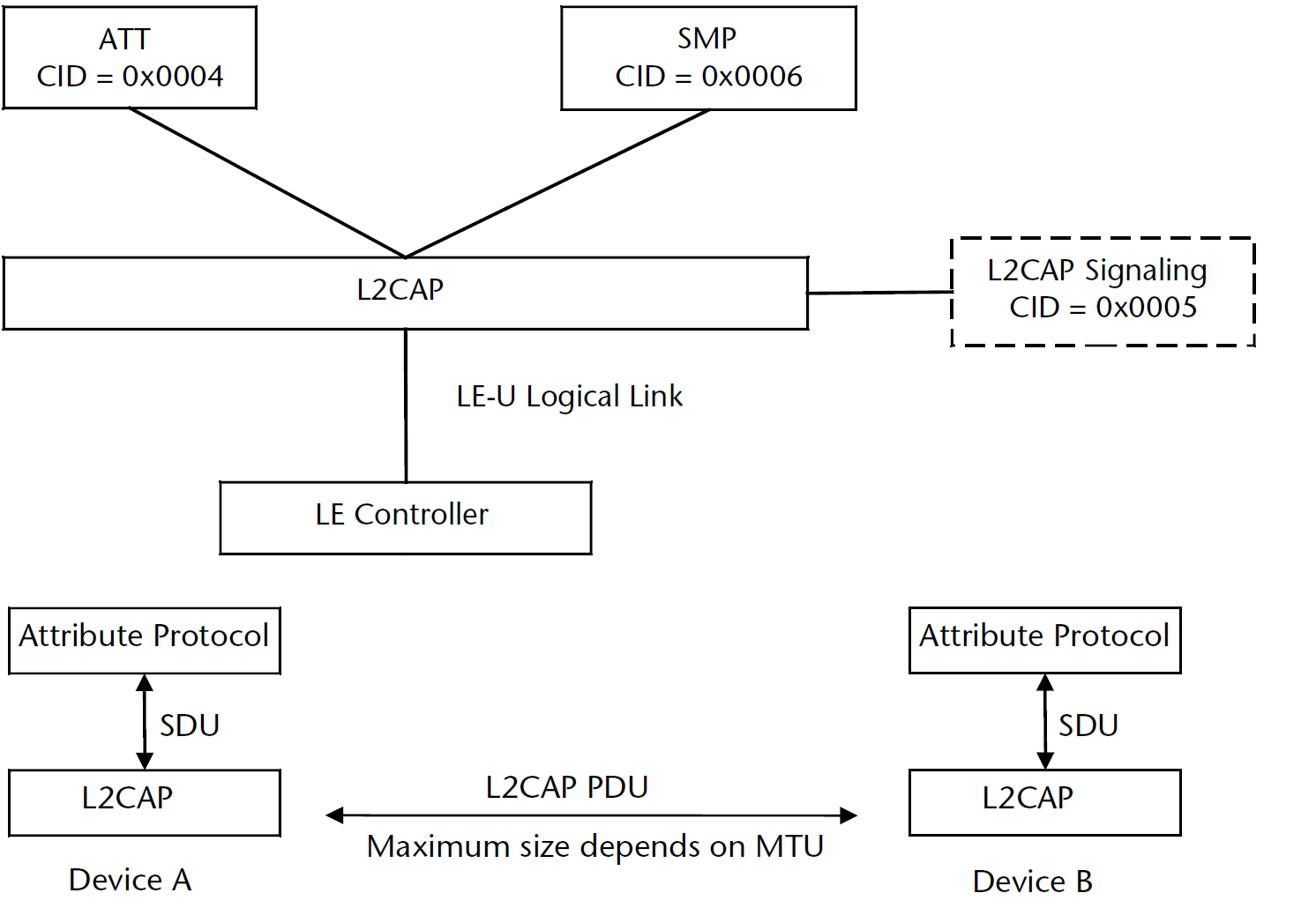
As specified in BLE Spec, L2CAP is mainly used for data transfer between Controller and Host. Most work are finished in stack bottom layer with little involvement of user. User only needs to invoke the following APIs to set correspondingly.
Register L2CAP Data Processing Function
In the BLE SDK architecture, the Controller's data is interfaced with the Host via the HCI, and the data from the HCI to the Host is first processed at the L2CAP layer, using the following API to register this processing function.
void blc_l2cap_register_handler (void *p);
In BLE Slave applications such as 8208_ble_sample/8208_module, the functions in the SDK L2CAP layer that process Controller data are:
int blc_l2cap_packet_receive (u16 connHandle, u8 * p);
This function has been implemented in the protocol stack and it will parse the received data and transmit it upwards to ATT, SIG or SMP.
Initialization:
blc_l2cap_register_handler (blc_l2cap_packet_receive);
In the 8208 hci, only the slave controller is implemented. The blc_hci_sendACLData2Host function transmits the controller data to the BLE Host device via a hardware interface such as UART/USB.
int blc_hci_sendACLData2Host (u16 handle, u8 *p)
Initialization:
blc_l2cap_register_handler (blc_hci_sendACLData2Host);
Update connection parameters
(1) Slave requests for connection parameter update
In BLE stack, Slave can actively apply for a new set of connection parameters by sending a “CONNECTION PARAMETER UPDATE REQUEST” command to Master in L2CAP layer. The figure below shows the command format. Please refer to “Core_v5.0” (Vol 3/Part A/ 4.20 “CONNECTION PARAMETER UPDATE REQUEST”).

The BLE SDK provides an API for slaves to actively apply to update connection parameters on the L2CAP layer to send the above CONNECTION PARAMETER UPDATE REQUEST command to the master.
void bls_l2cap_requestConnParamUpdate (u16 min_interval, u16 max_interval, u16 latency, u16 timeout);
The four parameters of this API correspond to the parameters in the “data” field of the “CONNECTION PARAMETER UPDATE REQUEST”. The “min_interval” and “max_interval” are the actual interval time divided by 1.25ms (e.g. for 7.5ms connection interval, the value should be 6); the “timeout” is actual supervision timeout divided by 10ms (e.g. for 1s timeout, the value should be 100).
Application example: Slave requests for new connection parameters when connection is established.
void    task_connect (u8 e, u8 *p, int n)
    {
        bls_l2cap_requestConnParamUpdate (6, 6, 99, 400);
        bls_l2cap_setMinimalUpdateReqSendingTime_after_connCreate(1000);
    }

The API:
void bls_l2cap_setMinimalUpdateReqSendingTime_after_connCreate(int time_ms)
serves to make the Slave wait for time_ms miliseconds after connection is established, and then invoke the API “bls_l2cap_requestConnParamUpdate” to update connection parameters. After conection is established, if user only invokes the “bls_l2cap_requestConnParamUpdate”, the Slave will wait for 1s to execute this request command.
(2) Master responds to connection parameter update request
After Master receives the “CONNECTION PARAMETER UPDATE REQUEST” command from Slave, it will respond with a “CONNECTION PARAMETER UPDATE RESPONSE” command. Please refer to “Core_v5.0” (Vol 3/Part A/ 4.20 “CONNECTION PARAMETER UPDATE RESPONSE”).
The figure below shows the command format: if “result” is “0x0000”, it indicates the request command is accepted; if “result” is “0x0001”, it indicates the request command is rejected.
Whether actual Android/iOS device will accept or reject the connection parameter update request is determined by corresponding BLE Master. User can refer to Master compatibility test.
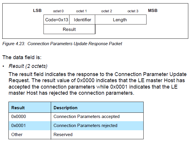
(3) Master updates connection parameters in Link Layer
After Master responds with “conn para update rsp” to accept the “conn para update req” from Slave, Master will send a “LL_CONNECTION_UPDATE_REQ” command in Link Layer.

Slave will mark the final parameter as the instant value of Master after it receives the update request. When the instant value of Slave reaches this value, connection parameters are updated, and the callback of the event “BLT_EV_FLAG_CONN_PARA_UPDATE” is triggered.
The “instant” indicates connection event count value maintained by Master and Slave, and it ranges from 0x0000 to 0xffff. During a connection, Master and Slave should always have consistent “instant” value. When Master sends “conn_req” and establishes connection with Slave, Master switches state from scanning to connection, and clears the “instant” of Master to “0”. When Slave receives the “conn_req”, it switches state from advertising to connection, and clears the instant of Slave to “0”. Each connection packet of Master and Slave is a connection event. For the first connection event after the “conn_req”, the instant value is “1”; for the second connection event, the instant value is 2, and so on.
When Master sends a “LL_CONNECTION_UPDATE_REQ”, the final parameter “instant” indicates during the connection event marked with “instant”, Master will use the values corresponding to the former connection parameters of the “LL_CONNECTION_UPDATE_REQ” packet. After the “LL_CONNECTION_UPDATE_REQ” is received, the new connection parameters will be used during the connection event when the instant of Slave equals the declared instant of Master, thus Slave and Master can finish switch of connection parameters synchronously.
ATT and GATT
GATT basic unit “Attribute”
GATT defines two roles: Server and Client. In this BLE SDK, Slave is Server, and corresponding Android/iOS device is Client. Server needs to supply multiple Services for Client to access.
Each Service of GATT consists of multiple Attributes, and each Attribute contains certain information. When multiple Attributes of different kinds are combined together, they can reflect a basic service.
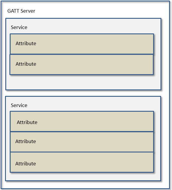
The basic contents of Attribute are shown as below:
(1) Attribute Type: UUID
The UUID is used to identify Attribute type, and its total length is 16 bytes. In BLE standard protocol, the UUID length is defined as two bytes, since Master devices follow the same method to transform 2-byte UUID into 16 bytes.
When standard 2-byte UUID is directly used, Master should know device types indicated by various UUIDs. 8x5x BLE stack defines some standard UUIDs in "stack/ble/service/hids.h" and "stack/service/uuid.h".
Telink proprietary profiles (OTA, MIC, SPEAKER, and etc.) are not supported in standard Bluetooth. The 16-byte proprietary device UUIDs are defined in “stack/ble/uuid.h”.
(2) Attribute Handle
Slave supports multiple Attributes which compose an Attribute Table. In Attribute Table, each Attribute is identified by an Attribute Handle value. After connection is established, Master will analyze and obtain the Attribute Table of Slave via “Service Discovery” process, then it can identify Attribute data via the Attribute Handle during data transfer.
(3) Attribute Value
Attribute Value corresponding to each Attribute is used as request, response, notification and indication data. In 8x5x BLE stack, Attribute Value is indicated by one pointer and the length of the area pointed by the pointer.
Attribute and ATT Table
To implement GATT Service on Slave, an Attribute Table is defined in this BLE SDK and it consists of multiple basic Attributes. Attribute definition is shown as below.
typedef struct attribute
    {
        u16 attNum;
        u8   perm;
        u8   uuidLen;
        u32  attrLen;    //4 bytes aligned
        u8*  uuid;
        u8*  pAttrValue;
        att_readwrite_callback_t  w;
        att_readwrite_callback_t  r;
    } attribute_t;
Below is Attribute Table given by the BLE SDK to illustrate the meaning of the above items. See app_att.c for the Attribute Table code, as shown below:
static const attribute_t my_Attributes[] = {
    {ATT_END_H - 1, 0,0,0,0,0}, // total num of attribute
    // 0001 - 0007  gap
    {7,ATT_PERMISSIONS_READ,2,2,(u8*)(&my_primaryServiceUUID),  (u8*)(&my_gapServiceUUID), 0},
    {0,ATT_PERMISSIONS_READ,2,sizeof(my_devNameCharVal),(u8*)(&my_characterUUID), (u8*)(my_devNameCharVal), 0},
    {0,ATT_PERMISSIONS_READ,2,sizeof(my_devName), (u8*)(&my_devNameUUID), (u8*)(my_devName), 0},
    {0,ATT_PERMISSIONS_READ,2,sizeof(my_appearanceCharVal),(u8*)(&my_characterUUID), (u8*)(my_appearanceCharVal), 0},
    {0,ATT_PERMISSIONS_READ,2,sizeof (my_appearance), (u8*)(&my_appearanceUIID),    (u8*)(&my_appearance), 0},
    {0,ATT_PERMISSIONS_READ,2,sizeof(my_periConnParamCharVal),(u8*)(&my_characterUUID), (u8*)(my_periConnParamCharVal), 0},
    {0,ATT_PERMISSIONS_READ,2,sizeof (my_periConnParameters),(u8*)(&my_periConnParamUUID),  (u8*)(&my_periConnParameters), 0},
    // 0008 - 000b gatt
    {4,ATT_PERMISSIONS_READ,2,2,(u8*)(&my_primaryServiceUUID),  (u8*)(&my_gattServiceUUID), 0},
    {0,ATT_PERMISSIONS_READ,2,sizeof(my_serviceChangeCharVal),(u8*)(&my_characterUUID),         (u8*)(my_serviceChangeCharVal), 0},
    {0,ATT_PERMISSIONS_READ,2,sizeof (serviceChangeVal), (u8*)(&serviceChangeUUID),     (u8*)(&serviceChangeVal), 0},
    {0,ATT_PERMISSIONS_RDWR,2,sizeof (serviceChangeCCC),(u8*)(&clientCharacterCfgUUID), (u8*)(serviceChangeCCC), 0},
};
Note: The key word “const” is added before Attribute Table definition:
const attribute_t my_Attributes[] = { ... };
By adding the “const”, the compiler will store the array data to flash rather than RAM, while all contents of the Attribute Table defined in flash are read only and not modifiable.
(1) attNum
The “attNum” supports two functions.
The “attNum” can be used to indicate the number of valid Attributes in current Attribute Table, i.e. the maximum Attribute Handle value. This number is only used in the invalid Attribute item 0 of Attribute Table array.
{57,0,0,0,0,0}, // ATT_END_H – 1 = 57
“attNum = 57” indicates there are 57 valid Attributes in current Attribute Table.
In BLE, Attribute Handle value starts from 0x0001 with increment step of 1, while the array index starts from 0. When this virtual Attribute is added to the Attribute Table, each Attribute index equals its Attribute Handle value. After the Attribute Table is defined, Attribute Handle value of an Attribute can be obtained by counting its index in current Attribute Table array.
The final index is the number of valid Attributes (i.e. attNum) in current Attribute Table. In current SDK, the attNum is set as 57; if user adds or deletes any Attribute, the attNum needs to be modified correspondingly.
The “attNum” can also be used to specify Attributes constituting current Service.
The UUID of the first Attribute for each Service must be “GATT_UUID_PRIMARY_SERVICE(0x2800)”; the first Attribute of a Service sets “attNum” and it indicates following “attNum” Attributes constitute current Service.
As shown in code above, for the gap service, the Attribute with UUID of “GATT_UUID_PRIMARY_SERVICE” sets the “attNum” as 7, it indicates the seven Attributes from Attribute Handle 1 to Attribute Handle 7 constitute the gap service.
Except for Attribute item 0 and the first Attribute of each Service, attNum values of all Attributes must be set as 0.
(2) perm
The “perm” is the simplified form of “permission” and it serves to specify access permission of current Attribute by Client.
The “perm” of each Attribute should be configured as one or combination of following 10 values.
#define ATT_PERMISSIONS_READ                 0x01
#define ATT_PERMISSIONS_WRITE                0x02
#define ATT_PERMISSIONS_AUTHEN_READ          0x61
#define ATT_PERMISSIONS_AUTHEN_WRITE         0x62
#define ATT_PERMISSIONS_SECURE_CONN_READ     0xE1
#define ATT_PERMISSIONS_SECURE_CONN_WRITE    0xE2
#define ATT_PERMISSIONS_AUTHOR_READ          0x11
#define ATT_PERMISSIONS_AUTHOR_WRITE         0x12
#define ATT_PERMISSIONS_ENCRYPT_READ         0x21
#define ATT_PERMISSIONS_ENCRYPT_WRITE        0x22
Note:
Current SDK version does not support PERMISSION READ and PERMISSION WRITE yet.
(3) uuid and uuidLen
As introduced above, UUID supports two types: BLE standard 2-byte UUID, and Telink proprietary 16-byte UUID. The “uuid” and “uuidLen” can be used to describe the two UUID types simultaneously.
The “uuid” is an u8-type pointer, and “uuidLen” specifies current UUID length, i.e. the uuidLen bytes starting from the pointer are current UUID. Since Attribute Table and all UUIDs are stored in flash, the “uuid” is a pointer pointing to flash.
a) BLE standard 2-byte UUID:
For example, the Attribute “devNameCharacter” with Attribute Handle of 2, related code is shown as below:
#define GATT_UUID_CHARACTER              0x2803
static const u16 my_characterUUID = GATT_UUID_CHARACTER;
static const u8 my_devNameCharVal[5] = {0x12, 0x03, 0x00, 0x00, 0x2A};
{0,1,2,5,(u8*)(&my_characterUUID), (u8*)(my_devNameCharVal), 0},
“UUID=0x2803” indicates “character” in BLE and the “uuid” points to the address of “my_devNameCharVal” in flash. The “uuidLen” is 2. When Master reads this Attribute, the UUID would be “0x2803”.
b) Telink proprietary 16-byte UUID:
For example, the Attribute MIC of audio, related code is shown as below:
#define TELINK_MIC_DATA {0x18,0x2B,0x0d,0x0c,0x0b,0x0a,0x09,0x08,0x07,0x06,0x05,0x04,0x03,0x02,0x01,0x0}
const u8 my_MicUUID[16]     = TELINK_MIC_DATA;
static u8 my_MicData        = 0x80;
{0,1,16,1,(u8*)(&my_MicUUID), (u8*)(&my_MicData), 0},
The “uuid” points to the address of “my_MicData” in flash, and the “uuidLen” is 16. When Master reads this Attribute, the UUID would be “0x000102030405060708090a0b0c0d2b18”.
(4) pAttrValue and attrLen
Each Attribute corresponds to an Attribute Value. The “pAttrValue” is an u8-type pointer which points to starting address of Attribute Value in RAM/Flash, while the “attrLen” specifies the data length. When Master reads the Attribute Value of certain Attribute from Slave, the “attrLen” bytes of data starting from the area (RAM/Flash) pointed by the “pAttrValue” will be read by this BLE SDK to Master.
Since UUID is read only, the “uuid” is a pointer pointing to flash; while Attribute Value may involve write operation into RAM, so the “pAttrValue” may points to RAM or flash.
For example, the Attribute hid Information with Attribute Handle of 35, related code is as shown below:
const u8 hidInformation[] =
{
    U16_LO(0x0111), U16_HI(0x0111),   // bcdHID (USB HID version),0x11,0x01
    0x00,                           // bCountryCode
    0x01                           // Flags
};
{0,1,2, sizeof(hidInformation),(u8*)(&hidinformationUUID), (u8*)(hidInformation), 0},
In actual application, the key word “const” can be used to store the read-only 4-byte hid information “0x01 0x00 0x01 0x11” into flash. The “pAttrValue” points to the starting address of hidInformation in flash, while the “attrLen” is the actual length of hidInformation. When Master reads this Attribute, “0x01000111” will be returned to Master correspondingly.
Figure below shows a packet example captured by BLE sniffer when Master reads this Attribute. Master uses the “ATT_Read_Req” command to set the target AttHandle as 0x23 (35), corresponding to the hid information in Attribute Table of SDK.

For the Attribute “battery value” with Attribute Handle of 40, related code is as shown below:
u8  my_batVal[1]    = {99};
{0,1,2,1,(u8*)(&my_batCharUUID),    (u8*)(my_batVal), 0},
In actual application, the “my_batVal” indicates current battery level and it will be updated according to ADC sampling result; then Slave will actively notify or Master will actively read to transfer the “my_batVal” to Master. The starting address of the “my_batVal” stored in RAM will be pointed by the “pAttrValue”.
In addition, when the att table exists CHARACTERISTIC_UUID_HID_REPORT_MAP, many devices need to identify the operating system, and then send different report maps according to the operating system, so the underlying layer can re-register the corresponding pAttrValue and attrLen when processing, the API interface is as follows.
ble_sts_t bls_att_setHIDReportMap(u8* p,u32 len);
If you need to restore the preset values defined in the Attribute Table, call the following API interface.
ble_sts_t bls_att_resetHIDReportMap();
(5) Callback function w
The callback function w is write function with prototype as below:
typedef int (*att_readwrite_callback_t)(u16 connHandle, void* p);
User must follow the format above to define callback write function. The callback function w is optional, i.e. for an Attribute, user can select whether to set the callback write function as needed (null pointer 0 indicates not setting callback write function).
The trigger condition for callback function w is: When Slave receives any Attribute PDU with Attribute Opcode as shown below, Slave will check whether the callback function w is set.
a) opcode = 0x12, Write Request.
b) opcode = 0x52, Write Command.
c) opcode = 0x18, Execute Write Request.
After Slave receives a write command above, if the callback function w is not set, Slave will automatically write the area pointed by the “pAttrValue” with the value sent from Master, and the data length equals the “l2capLen” in Master packet format minus 3; if the callback function w is set, Slave will execute user-defined callback function w after it receives the write command, rather than writing data into the area pointed by the “pAttrValue”. Note: Only one of the two write operations is allowed to take effect.
By setting the callback function w, user can process Write Request, Write Command, and Execute Write Request in ATT layer of Master. If the callback function w is not set, user needs to evaluate whether the area pointed by the “pAttrValue” can process the command (e.g. If the “pAttrValue” points to flash, write operation is not allowed; or if the “attrLen” is not long enough for Master write operation, some data will be modified unexpectedly). In addition, the return value of the callback function w is 0, which means that the write was successful. For other return values, please refer to the enumeration att_err_t or define it by the user according to the protocol requirements.
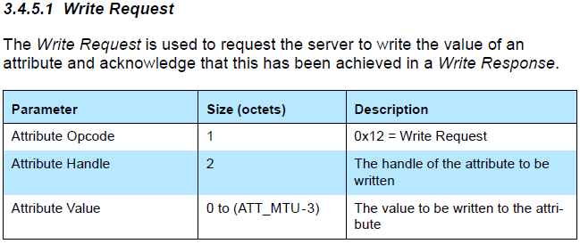
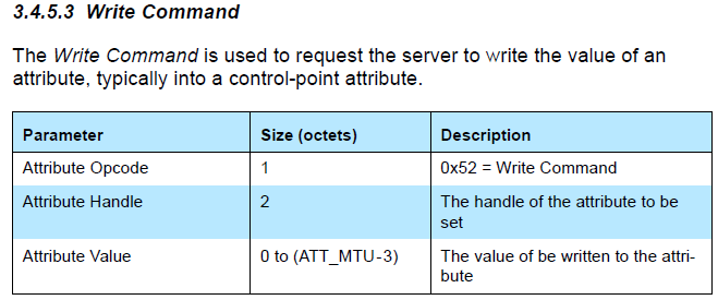

The void-type pointer “p” of the callback function w points to the value of Master write command. Actually “p” points to a memory area, the value of which is shown as the following structure.
typedef struct{
    u8  type;
    u8  rf_len;
    u16 l2capLen;
    u16 chanId;
    u8  opcode;
    u16 handle;
    u8  dat[20];
}rf_packet_att_data_t;
“p” points to "type", valid length of data is l2cap minus 3, and the first valid data is p->dat[0].
int my_WriteCallback (void *p)
{
    rf_packet_att_data_t *pw = (rf_packet_att_data_t *)p;
    int len = pw->l2cap - 3;
    //add your code
    //valid data is pw->dat[0] ~ pw->dat[len-1]
    return 0;
}
The structure “rf_packet_att_data_t” above is available in the “stack/ble/ble_format.h”.
(6) Callback function r
The callback function r is read function with prototype as below:
typedef int (*att_readwrite_callback_t)(u16 connHandle,void* p);
User must follow the format above to define callback read function. The callback function r is also optional, i.e. for an Attribute, user can select whether to set the callback read function as needed (null pointer 0 indicates not setting callback read function), connHandle is connecting sentence between master and slave, type BLS_CONN_HANDLE for slave application, and type BLM_CONN_HANDLE for master application.
The trigger condition for callback function r is: When Slave receives any Attribute PDU with Attribute Opcode as shown below, Slave will check whether the callback function r is set.
a) opcode = 0x0A, Read Request.
b) opcode = 0x0C, Read Blob Request.
After Slave receives a read command above,
a) If the callback read function is set, Slave will execute this function, and determine whether to respond with “Read Response/Read Blob Response” according to the return value of this function.
-
If the return value is 1, Slave won’t respond with “Read Response/Read Blob Response” to Master.
-
If the return value is not 1, Slave will automatically read “attrLen” bytes of data from the area pointed by the “pAttrValue”, and the data will be responded to Master via “Read Response/Read Blob Response”.
b) If the callback read function is not set, Slave will automatically read “attrLen” bytes of data from the area pointed by the “pAttrValue”, and the data will be responded to Master via “Read Response/Read Blob Response”.
Therefore, after a Read Request/Read Blob Request is received from Master, if it’s needed to modify the content of Read Response/Read Blob Response, user can register corresponding callback function r, modify contents in RAM pointed by the “pAttrValue” in this callback function, and the return value must be 0.
(7) Attribute Table layout
Figure below shows Service/Attribute layout based on Attribute Table. The “attnum” of the first Attribute indicates the number of valid Attributes in current ATT Table; the remaining Attributes are assigned to different Services, the first Attribute of each Service is the “declaration”, and the following “attnum” Attributes constitute current Service. Actually the first item of each Service is a Primary Service.
#define GATT_UUID_PRIMARY_SERVICE                    0x2800
const u16 my_primaryServiceUUID = GATT_UUID_PRIMARY_SERVICE;
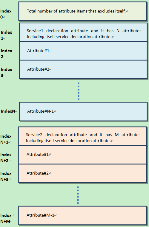
(8) ATT table Initialization
GATT & ATT initialization only needs to transfer the pointer of Attribute Table in APP layer to protocol stack, and the API below is supplied:
void bls_att_setAttributeTable (u8 *p);
“p” is the pointer of Attribute Table.
Attribute PDU and GATT API
As required by BLE spec, the following Attribute PDU types are supported in current SDK.
-
Requests: Data request sent from Client to Server.
-
Responses: Data response sent by Server after it receives request from Client.
-
Commands: Command sent from Client to Server.
-
Notifications: Data sent from Server to Client.
-
Indications: Data sent from Server to Client.
-
Confirmations: Confirmation sent from Client after it receives data from Server.
The following is an analysis of all ATT PDUs at the ATT layer in conjunction with the Attribute structure and Attribute Table structure described previously.
(1) Read by Group Type Request, Read by Group Type Response
Please refer to “Core_v5.0” (Vol 3/Part F/3.4.4.9 and 3.4.4.10) for details about the “Read by Group Type Request” and “Read by Group Type Response” commands.
The “Read by Group Type Request” command sent by Master specifies starting and ending attHandle, as well as attGroupType. After the request is received, Slave will check through current Attribute Table according to the specified starting and ending attHandle, and find the Attribute Group that matches the specified attGroupType. Then Slave will respond to Master with Attribute Group information via the “Read by Group Type Response” command.
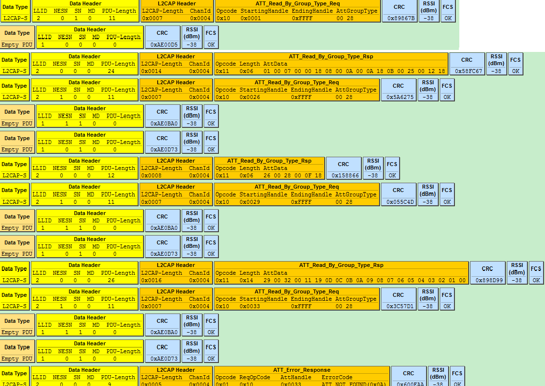
As shown above, Master requests from Slave for Attribute Group information of the “primaryServiceUUID” with UUID of 0x2800.
#define GATT_UUID_PRIMARY_SERVICE        0x2800
const u16 my_primaryServiceUUID = GATT_UUID_PRIMARY_SERVICE;
The following groups in Slave Attribute Table meet the requirement according to current demo code.
a) Attribute Group with attHandle from 0x0001 to 0x0007,
Attribute Value is SERVICE_UUID_GENERIC_ACCESS (0x1800).
b) Attribute Group with attHandle from 0x0008 to 0x000a,
Attribute Value is SERVICE_UUID_DEVICE_INFORMATION (0x180A).
c) Attribute Group with attHandle from 0x000B to 0x0025,
Attribute Value is SERVICE_UUID_HUMAN_INTERFACE_DEVICE (0x1812).
d) Attribute Group with attHandle from 0x0026 to 0x0028,
Attribute Value is SERVICE_UUID_BATTERY (0x180F).
e) Attribute Group with attHandle from 0x0029 to 0x0032,
Attribute Value is TELINK_AUDIO_UUID_SERVICE(0x11,0x19,0x0d,0x0c,0x0b,0x0a,0x09,0x08,0x07,0x06, 0x05,0x04,0x03,0x02,0x01,0x00).
Slave responds to Master with the attHandle and attValue information of the five Groups above via the “Read by Group Type Response” command. The final ATT_Error_Response indicates end of response. When Master receives this packet, it will stop sending “Read by Group Type Request”.
(2) Find by Type Value Request, Find by Type Value Response
Please refer to “Core_v5.0” (Vol 3/Part F/3.4.3.3 and 3.4.3.4) for details about the “Find by Type Value Request” and “Find by Type Value Response” commands.
The “Find by Type Value Request” command sent by Master specifies starting and ending attHandle, as well as AttributeType and Attribute Value. After the request is received, Slave will check through current Attribute Table according to the specified starting and ending attHandle, and find the Attribute that matches the specified AttributeType and Attribute Value. Then Slave will respond to Master with the Attribute via the “Find by Type Value Response” command.

(3) Read by Type Request, Read by Type Response
Please refer to “Core_v5.0” (Vol 3/Part F/3.4.4.1 and 3.4.4.2) for details about the “Read by Type Request” and “Read by Type Response” commands.
The “Read by Type Request” command sent by Master specifies starting and ending attHandle, as well as AttributeType. After the request is received, Slave will check through current Attribute Table according to the specified starting and ending attHandle, and find the Attribute that matches the specified AttributeType. Then Slave will respond to Master with the Attribute via the “Read by Type Response”.
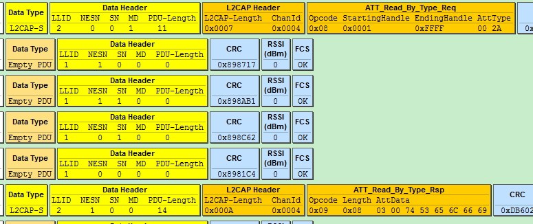
As shown above, Master reads the Attribute with attType of 0x2A00, i.e. the Attribute with Attribute Handle of 00 03 in Slave.
const u8    my_devName [] = {'t', 'S', 'e', 'l', 'f', 'i'};
#define GATT_UUID_DEVICE_NAME            0x2a00
const u16 my_devNameUUID = GATT_UUID_DEVICE_NAME;
{0,1,2, sizeof (my_devName),(u8*)(&my_devNameUUID),(u8*)(my_devName), 0},
In the “Read by Type response”, attData length is 8, the first two bytes are current attHandle “0003”, followed by 6-byte Attribute Value.
(4) Find information Request, Find information Response
Please refer to “Core_v5.0” (Vol 3/Part F/3.4.3.1 and 3.4.3.2) for details about the “Find information request” and “Find information response” commands.
The master sends a "Find information request", specifying the starting and ending attHandle. After receiving the command, the slave replies to the master through "Find information response" the UUIDs of all the starting and ending attHandle corresponding Attributes. As shown in the figure below, the master requires information of three Attributes with attHandle of 0x0016~0x0018, and Slave responds with corresponding UUIDs.

(5) Read Request, Read Response
Please refer to “Core_v5.0” (Vol 3/Part F/3.4.4.3 and 3.4.4.4) for details about the “Read Request” and “Read Response” commands.
The “Read Request” command sent by Master specifies certain attHandle. After the request is received, Slave will respond to Master with the Attribute Value of the specified Attribute via the “Read Response” command (If the callback function r is set, this function will be executed), as shown below.

(6) Read Blob Request, Read Blob Response
Please refer to “Core_v5.0” (Vol 3/Part F/3.4.4.5 and 3.4.4.6) for details about the “Read Blob Request” and “Read Blob Response” commands.
If some Slave Attribute corresponds to Attribute Value with length exceeding MTU_SIZE (It’s set as 23 in current SDK), Master needs to read the Attribute Value via the “Read Blob Request” command, so that the Attribute Value can be sent in packets. This command specifies the attHandle and ValueOffset. After the request is received, Slave will find corresponding Attribute, and respond to Master with the Attribute Value via the “Read Blob Response” command according to the specified ValueOffset. (If the callback function r is set, this function will be executed.)
As shown below, when Master needs the HID report map of Slave (report map length largely exceeds 23), first Master sends “Read Request”, then Slave responds to Master with part of the report map data via “Read response”; Master sends “Read Blob Request”, and then Slave responds to Master with data via “Read Blob Response”.
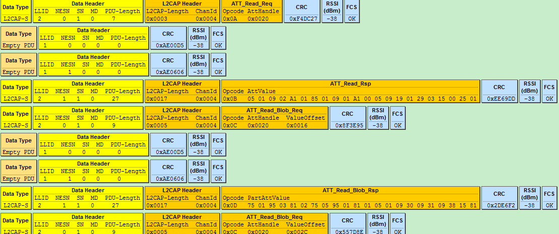
(7) Exchange MTU Request, Exchange MTU Response
Please refer to “Core_v5.0” (Vol 3/Part F/3.4.2.1 and 3.4.2.2) for details about the “Exchange MTU Request” and “Exchange MTU Response” commands.
As shown below, Master and Slave obtain MTU size of each other via the “Exchange MTU Request” and “Exchange MTU Response” commands.

During data access process of Telink BLE Slave GATT layer, if there’s data exceeding a RF packet length, which involves packet assembly and disassembly in GATT layer, Slave and Master need to exchange RX MTU size of each other in advance. Transfer of long packet data in GATT layer can be implemented via MTU size exchange.
a) User can register callback of GAP event and enable the eventMask “GAP_EVT_MASK_ATT_EXCHANGE_MTU” to obtain EffectiveRxMTU.
EffectiveRxMTU=min(ClientRxMTU, ServerRxMTU)。
The “GAP event” section of this document will introduce GAP event in detail.
b) Processing of long Rx packet data in Slave GATT layer
B80 Slave ServerRxMTU is set as 23 by default. Actually maximum ServerRxMTU can reach 250, i.e. 250-byte packet data on Master can be correctly re-assembled on Slave. When it’s needed to use packet re-assembly of Master in an application, the API below should be invoked to modify RX size of Slave first.
ble_sts_t blc_att_setRxMtuSize(u16 mtu_size);
The return value is shown as below:
| ble_sts_t | Value | ERR Reason |
|---|---|---|
| BLE_SUCCESS | 0 | Add success |
| GATT_ERR_INVALID_ PARAMETER | See the definition in the SDK | mtu_size exceeds the max value 250. |
When Master GATT layer needs to send long packet data to Slave, Master will actively initiate “ATT_Exchange_MTU_req”, and Slave will respond with “ATT_Exchange_MTU_rsp”. “ServerRxMTU” is the configured value of the API “blc_att_setRxMtuSize”. If user has registered GAP event and enabled the eventMask “GAP_EVT_MASK_ATT_EXCHANGE_MTU”, “EffectiveRxMTU” and “ClientRxMTU” of Master can be obtained in the callback function of GAP event.
c) Processing of long Tx packet data in Slave GATT layer
When B80 Slave needs to send long packet data in GATT layer, it should obtain Client RxMTU of Master first, and the eventual data length should not exceed ClientRxMTU.
First Slave should invoke the API “blc_att_setRxMtuSize” to set its ServerRxMTU. Suppose it’s set as 158.
blc_att_setRxMtuSize(158);
Then the API below should be invoked to actively initiate an “ATT_Exchange_MTU_req”.
ble_sts_t blc_att_requestMtuSizeExchange (u16 connHandle, u16 mtu_size);
“connHandle” is ID of Slave conection, i.e. “BLS_CONN_HANDLE”, while “mtu_size” is ServerRxMTU.
blc_att_requestMtuSizeExchange(BLS_CONN_HANDLE, 158);
After the “ATT_Exchange_MTU_req” is received, Master will respond with “ATT_Exchange_MTU_rsp”. After receiving the response, the SDK will calculate EffectiveRxMTU. If user has registered GAP event and enabled the eventMask “GAP_EVT_MASK_ATT_EXCHANGE_MTU”, “EffectiveRxMTU” and “ClientRxMTU” will be reported to user.
(8) Write Request, Write Response
Please refer to “Core_v5.0” (Vol 3/Part F/3.4.5.1 and 3.4.5.2) for details about the “Write Request” and “Write Response” commands.
The “Write Request” command sent by Master specifies certain attHandle and attaches related data. After the request is received, Slave will find the specified Attribute, determine whether to process the data by using the callback function w or directly write the data into corresponding Attribute Value depending on whether the callback function w is set by user. Finally Slave will respond to Master via “Write Response”.
As shown in below, by sending “Write Request”, Master writes Attribute Value of 0x0001 to the Slave Attribute with the attHandle of 0x0016. Then Slave will execute the write operation and respond to Master via “Write Response”.

(9) Write Command
Please refer to “Core_v5.0” (Vol 3/Part F/3.4.5.3) for details about the “Write Command”.
The “Write Command” sent by Master specifies certain attHandle and attaches related data. After the command is received, Slave will find the specified Attribute, determine whether to process the data by using the callback function w or directly write the data into corresponding Attribute Value depending on whether the callback function w is set by user. Slave won’t respond to Master with any information.
(10) Queued Writes
“Queued Writes” refers to ATT protocol including “Prepare Write Request/Response” and “Execute Write Request/Response”. Please refer to “Core_v5.0” (Vol 3/Part F/3.4.6/Queued Writes).
“Prepare Write Request” and “Execute Write Request” can implement the two functions below.
a) Provide write function for long attribute value.
b) Allow to write multiple values in an atomic operation that is executed seperately.
Similar to “Read_Blob_Req/Rsp”, “Prepare Write Request” contains AttHandle, ValueOffset and PartAttValue. That means Client can prepare multiple attribute values or various parts of a long attribute value in the queue. Thus, before executing the prepared queue indeed, Client can confirm that all parts of some attribute can be written into Server.
Note: Current SDK version only supports the write function of long attribute value with the maximum length not exceeding 244 bytes. If the length is greater than 244 bytes, the following API interface needs to be called to make changes to the prepare write buffer and its length.
void blc_att_setPrepareWriteBuffer(u8 *p, u16 len)
The figure below shows the case when Master writes a long character string “I am not sure what a new song” (byte number is far more than 23, and use the default MTU) into certain characteristic of Slave. First Master sends a “Prepare Write Request” with offset of 0x0000, to write the data “I am not sure what” into Slave, and Slave responds to Master with a “Prepare Write Response”. Then Master sends a “Prepare Write Request” with offset of 0x12, to write the data “ a new song” into Slave, and Slave responds to Master with a “Prepare Write Response”. After the write operation of the long attribute value is finished, Master sends an “Execute Write Request” to Slave. “Flags=1” indicates write result takes effect immediately. Then Slave responds with an “Execute Write Response” to complete the whole Prepare Write process.
As we can see, “Prepare Write Response” also contains AttHandle, ValueOffsetand PartAttValue in the request, so as to ensure reliable data transfer. Client can compare field value of Response with that of Request, to ensure correct reception of the prepared data.
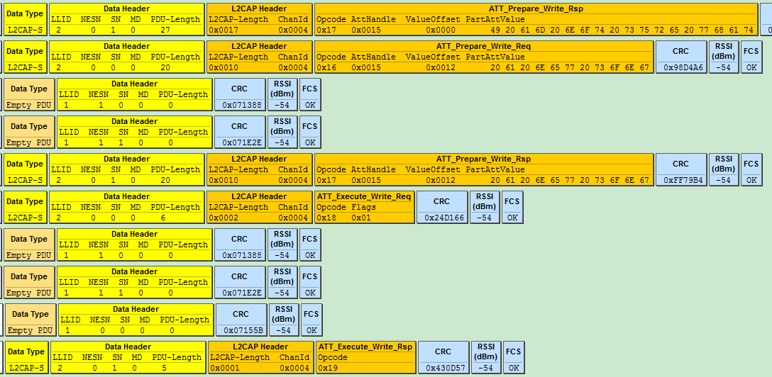
(11) Handle Value Notification
Please refer to “Core_v5.0” (Vol 3/Part F/3.4.7.1).

The figure above shows the format of “Handle Value Notification” in BLE Spec.
This BLE SDK supplies an API for Handle Value Notification of an Attribute. By invoking this API, user can push the notify data into bottom-layer BLE software fifo. Stack will push the data of software fifo into hardware fifo during the latest packet transfer interval, and finally send the data out via RF.
ble_sts_t blc_gatt_pushHandleValueNotify (u16 handle, u8 *p, int len);
The handle is the attHandle of the corresponding Attribute, p is the header pointer to the contiguous memory data to be sent, and len specifies the number of bytes of data to be sent. Since this API supports auto packet disassembly based on EffectiveMaxTxOctets, long indicate data to be sent can be disassembled into multiple BLE RF packets, large “len” is supported. (EffectiveMaxTxOctets indicates the maximum RF TX octets to be sent in the Link Layer. Its default value is 27, and DLE may modify it. Another API as a replacement will be introduced later.)
When Link Layer is in Conn state, generally data will be successfully pushed into bottom-layer software FIFO by invoking this API; however, some special cases may result in invoking failure, and the return value “ble_sts_t” will indicate the corresponding error reason.
When this API is invoked in APP layer, it’s recommended to check whether the return value is “BLE_SUCCESS”. If the return value is not “BLE_SUCCESS”, a delay is needed to re-push the data.
The return value is shown as below:
| ble_sts_t | Value | ERR Reason |
|---|---|---|
| BLE_SUCCESS | 0 | Success |
| LL_ERR_CONNECTION_NOT_ ESTABLISH | See the definition in the SDK | Link Layer is in None Conn state |
| SMP_ERR_PAIRING_BUSY | See the definition in the SDK | Data cannot be sent during pairing phase. |
| LL_ERR_ENCRYPTION_BUSY | See the definition in the SDK | Data cannot be sent during encryption phase. |
| LL_ERR_TX_FIFO_NOT_ ENOUGH | See the definition in the SDK | Since task with mass data is being executed, software Tx fifo is not enough. |
| GATT_ERR_DATA_LENGTH_ EXCEED_MTU_SIZE | See the definition in the SDK | When len is greater than ATT_MTU-3, the transmitted data length exceeds the maximum data length supported by the ATT layer. |
| GATT_ERR_DATA_PENDING_ DUE_TO_SERVICE_DISCOVERY _BUSY | See the definition in the SDK | Data cannot be sent during service discovery phase. |
(12) Handle Value Indication
Please refer to “Core_v5.0” (Vol 3/Part F/3.4.7.2).

The figure above shows the format of “Handle Value Indication” in BLE Spec.
This BLE SDK supplies an API for Handle Value Indication of an Attribute. By invoking this API, user can push the indicate data into bottom-layer BLE software fifo. Stack will push the data of software fifo into hardware fifo during the latest packet transfer interval, and finally send the data out via RF.
ble_sts_t blc_gatt_pushHandleValueIndicate(u16 connHandle, u16 attHandle, u8 *p, int len);
The atthandle is the attHandle of the corresponding Attribute, p is the header pointer to the contiguous memory data to be sent, and len specifies the number of bytes of data to be sent. Since this API supports auto packet disassembly based on EffectiveMaxTxOctets, long indicate data to be sent can be disassembled into multiple BLE RF packets, large “len” is supported. (EffectiveMaxTxOctets indicates the maximum RF TX octets to be sent in the Link Layer. Its default value is 27, and DLE may modify it. Another API as a replacement will be introduced later.)
The BLE Spec states that each indicate cannot be considered successful until the Master confirms it, and the next indicate cannot be sent without success.
When Link Layer is in Conn state, generally data will be successfully pushed into bottom-layer software FIFO by invoking this API; however, some special cases may result in invoking failure, and the return value “ble_sts_t” will indicate the corresponding error reason. When this API is invoked in APP layer, it’s recommended to check whether the return value is “BLE_SUCCESS”. If the return value is not “BLE_SUCCESS”, a delay is needed to re-push the data.
The return value is shown as below:
| ble_sts_t | Value | ERR Reason |
|---|---|---|
| BLE_SUCCESS | 0 | Add success |
| LL_ERR_CONNECTION_ NOT_ESTABLISH | See the definition in the SDK | Link Layer is in None Conn state |
| SMP_ERR_PAIRING_BUSY | See the definition in the SDK | Data cannot be sent during pairing phase. |
| LL_ERR_ENCRYPTION_BUSY | See the definition in the SDK | Data cannot be sent during encryption phase. |
| LL_ERR_TX_FIFO_ NOT_ENOUGH | See the definition in the SDK | Since task with mass data is being executed, software Tx fifo is not enough. |
| GATT_ERR_DATA_PENDING _DUE_TO_SERVICE_DISCOVERY _BUSY | See the definition in the SDK | Data cannot be sent during service discovery phase. |
| GATT_ERR_PREVIOUS_ INDICATE_DATA_HAS_NOT_ CONFIRMED | See the definition in the SDK | The previous indicate data has not been confirmed by Master. |
| GATT_ERR_DATA_LENGTH _EXCEED_MTU_SIZE | See the definition in the SDK | When len is greater than ATT_MTU-3, the transmitted data length exceeds the maximum data length supported by the ATT layer. |
(13) Handle Value Confirmation
The details of Handle Value Confirmation refers to “Core_v5.0” (Vol 3/Part F/3.4.7.3).
Whenever the API “bls_att_pushIndicateData” (or “blc_gatt_pushHandleValueIndicate”) is invoked by APP layer to send an indicate data to Master, Master will respond with “Confirmation” to confirm the data, then Slave can continue to send the next indicate data.

As shown above, “Confirmation” is not specific to indicate data of certain handle, and the same “Confirmation” will be responded irrespective of handle.
To enable the APP layer to know whether the indicate data has already been confirmed by Master, user can register the callback of GAP event (see section 3.3.5.2 GAP event), and enable corresponding eventMask “GAP_EVT_GATT_HANDLE_VLAUE_CONFIRM” to obtain Confirm event.
GATT Service Security
Before reading “GATT Service Security”, user can refer to section 3.3.4 SMP to learn basic knowledge related to SMP including LE pairing method, security level, and etc.
The figure below shows the mapping relationship of service request for GATT Service Security level given by BLE spec. Please refer to “core5.0” (Vol3/Part C/10.3 AUTHENTICATION PROCEDURE).
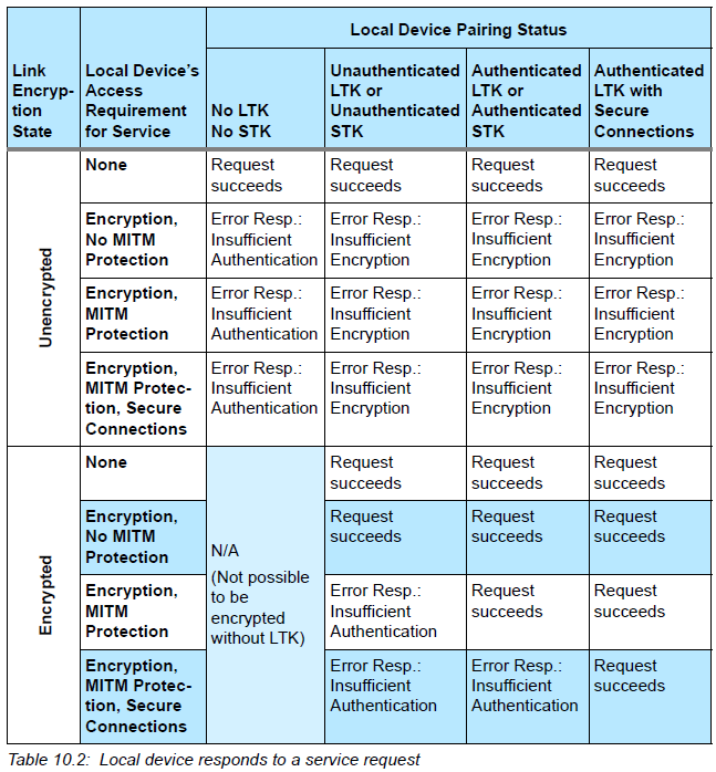
As shown in the figure above:
-
The first column marks whether currently connected Slave device is in encryption state;
-
The second column (local Device’s Access Requirement for service) is related to Permission Access setting for attributes in ATT table;
-
The third column includes four sub-columns corresponding to four levels of LE secuiry mode1 for current device pairing state:
(1) No authentication and no encryption
(2) Unauthenticated pairing with encryption
(3) Authenticated pairing with encryption
(4) Authenticated LE Secure Connections
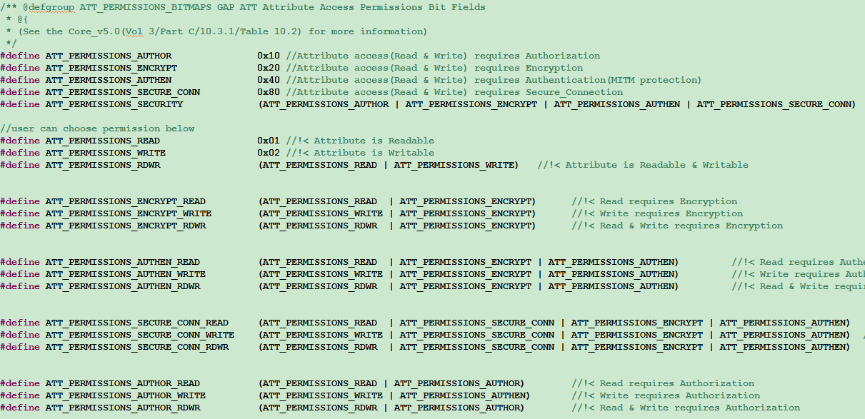
The final implementation of GATT Service Security is related to parameter settings during SMP initialization, including the highest security level, permission access of attributes in ATT table. It is also related to Master, for example, suppose Slave sets the highest security level supported by SMP as “Authenticated pairing with encryption”, but the highest level supported by Master is “Unauthenticated pairing with encryption”; if the permission for some write attribute in ATT table is “ATT_PERMISSIONS_AUTHEN_WRITE”, when Master writes this attribute, an error will be responded to indicate “encryption level is not enough”.
User can set permission of attributes in ATT table to implement the application below:
Suppose the highest security level supported by Slave is “Unauthenticated pairing with encryption”, but it’s not hoped to trigger Master pairing by sending “Security Request” after connection, user can set the permission for CCC (Client Characteristic Configuration) attribute with nofity attribute as “ATT_PERMISSIONS_ENCRYPT_WRITE”. Only when Master writes the CCC, will Slave respond that security level is not enough and trigger Master to start pairing encryption.
Note:
Security level set by user only indicates the highest security level supported by device, and GATT Service Secuiry can be used to realize control as long as ATT Permission does not exceed the highest level that takes effect indeed. For LE security mode1 level 4, if use only sets the level “Authenticated LE Secure Connections”, the setting supports LE Secure Connections only.
For the example of GATT security level, please refer to "8208_feature/ feature_gatt_security/app.c".
SMP
Security Manager (SM) in BLE is mainly used to provide various encryption keys for LE device to ensure data security. Encrypted link can protect the original contents of data in the air from being intercepted, decoded or read by any attacker. For details about the SMP, please refer to “Core_v5.0” (Vol 3/Part H/ Security Manager Specification).
SMP Security Level
BLE 4.2 Spec adds a new pairing method “LE Secure Connections” which further strengthens security. The pairing method in earlier version is called “LE legacy pairing”.
Recalling the section "GATT service Security", the following types of pairing status are available for local devices.

The four states correspond to the four levels of LE security mode1, details refer to "Core_v5.0" (Vol 3//Part C/10.2 LE SECURITY MODES)
(1) No authentication and no encryption (LE security mode1 level1)
(2) Unauthenticated pairing with encryption (LE security mode1 level2)
(3) Authenticated pairing with encryption (LE security mode1 level3)
(4) Authenticated LE Secure Connections (LE security mode1 level4)
Note:
Security level set by local device only indicates the highest security level that local device may reach. However, to reach the preset level indeed, the two factors below are important:
a)The supported highest security level set by peer Master device >= the supported highest security level set by local Slave device.
b)Both local device and peer device complete the whole pairing process (if pairing exsits) correctly as per the preset SMP parameters.
For example, even if the highest security level supported by Slave is set as “mode1 level3” (Authenticated pairing with encryption), when the highest security level supported by peer Master is set as “mode1 level1” (No authentication and no encryption), after connection Slave and Master won’t execute pairing, and indeed Slave uses security mode1 level 1.
User can use the API below to set the highest security level supported by SM:
void blc_smp_setSecurityLevel(le_security_mode_level_t mode_level);
Following shows the definition for the enum type le_security_mode_level_t:
typedef enum {
    LE_Security_Mode_1_Level_1 = BIT(0),        No_Authentication_No_Encryption = BIT(0), No_Security = BIT(0),
    LE_Security_Mode_1_Level_2 = BIT(1),        Unauthenticated_Paring_with_Encryption = BIT(1),
    LE_Security_Mode_1_Level_3 = BIT(2),        Authenticated_Paring_with_Encryption = BIT(2),
    LE_Security_Mode_1_Level_4 = BIT(3),       Authenticated_LE_Secure_Connection_Paring_with_Encryption =BIT(3),
.....
}le_security_mode_level_t;
SMP Parameter Configuration
SMP parameter configuration In Telink BLE SDK is introduced according to the configuration of four SMP security levels. For Slave, SMP function currently can support the highest security level “LE security mode1 level4”; for master, currently the SMP function in the traditional pairing method can support the highest security level "LE security mode1 level2" (traditional pairing Just Works method).
(1) LE security mode1 level1
Level 1 indicates device does not support encryption pairing. If it’s needed to disable SMP function, user only needs to invoke the function below during initialization:
blc_smp_setSecurityLevel(No_Security);
It means the device won’t implement pairing encryption for current connection. Even if the peer requests for pairing encryption, the device will reject it. It generally applies to the device that does not support encryption pairing process. As shown in the figure below, Master sends a pairing request, and Slave responds with “SM_Pairing_Failed”.

(2) LE security mode1 level2
Level 2 indicates device supports the highest security level “Unauthenticated_Paring_with_Encryption”, e.g. “Just Works” pairing mode in legacy pairing and secure connection pairing method.
a) As introduced earlier, SMP supports legacy encryption and secure connection pairing. The SDK provides the API below to set whether the new encryption feature in BLE4.2 is supported.
void blc_smp_setParingMethods (paring_methods_t method);
Following shows the definition for the enum type paring_methods_t:
typedef enum {
    LE_Legacy_Paring     = 0,   // BLE 4.0/4.2
    LE_Secure_Connection = 1,   // BLE 4.2/5.0/5.1
}paring_methods_t;
b) When using security level other than LE security mode1 level1, the API below must be invoked to initialize SMP parameter configuration, including flash initialization setting of bonded area.
int blc_smp_peripheral_init (void);
If only this API is invoked during initialization, the SDK will use default parameters to configure SMP:
-
The highest security level supported by default: Unauthenticated_Paring_with_Encryption.
-
Default bonding mode: Bondable_Mode (store KEY that is distributed after pairing encryption into flash).
-
Default IO capability: IO_CAPABILITY_NO_INPUT_NO_OUTPUT.
The default parameters above follow the configuration of legacy pairing “Just Works” mode. Therefore invoking this API only is equivalent to configure LE security mode1 level2. LE security mode1 level2 has two types of setting:
a) Device supports initialization setting of “Just Works” in legacy pairing.
blc_smp_peripheral_init();
b) Device supports initialization setting of “Just Works” in secure connections.
blc_smp_setParingMethods(LE_Secure_Connection);
blc_smp_peripheral_init();
(3) LE security mode1 level3
Level 3 indicates device supports the highest security level “Authenticated pairing with encryption”, e.g. “Passkey Entry” / “Out of Band” in legacy pairing mode.
As required by this level, device should support Authentication, i.e. legal identity of two pairing sides should be ensured. The three Authentication methods below are supported in BLE:
-
Method 1 with involvement of user, e.g. device has button or display capability, so that one side can display TK, while the other side can input the same TK (e.g. Passkey Entry).
-
Method 2: The two pairing sides can exchange information using the method of non-BLE RF transfer to implement pairing (e.g. Out of Band which transfers TK via NFC generally).
-
Method 3: Use the TK negotiated and agreed by two device sides (e.g. Just Works with TK 0 used by two sides). Since this method is Unauthenticated, the security level of “Just Works” corresponds to LE security mode1 level2.
Authentication can ensure the legality of two pairing sides, and this protection method is called MITM (Man-in-the-Middle) protection.
a) Device with Authentication should set its MITM flag or OOB flag. The SDK provides the two APIs below to set MITM flag and OOB flag.
void blc_smp_enableAuthMITM (int MITM_en);
void blc_smp_enableOobAuthentication (int OOB_en);
“MITM_en”/“OOB_en”: 1 - enable; 0 - disable.
b) As introduced earlier, SM provides three Authentication methods selectable depending on IO capability of two sides. The SDK provides the API below to set IO capability for current device.
void blc_smp_setIoCapability (io_capability_t ioCapablility);
Following shows the definition for the enum type io_capability_t:
typedef enum {
    IO_CAPABILITY_UNKNOWN = 0xff,
    IO_CAPABILITY_DISPLAY_ONLY = 0,
    IO_CAPABILITY_DISPLAY_YESNO = 1,
    IO_CAPABILITY_KEYBOARD_ONLY = 2,
    IO_CAPABILITY_NO_IN_NO_OUT = 3,
    IO_CAPABILITY_KEYBOARD_DISPLAY = 4,
} io_capability_t;
c) The figure below shows the rule to use MITM flag and OOB flag in legacy pairing mode.
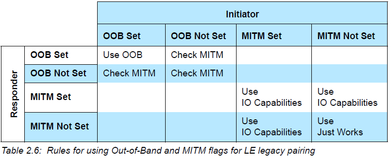
The OOB and MITM flag of local device and peer device will be checked to determine whether to use OOB method or select certain KEY generation method as per IO capability. As shown in the figure below, the SDK will select different KEY generation methods according to IO capability (Row/Column parameter type io_capability_t):
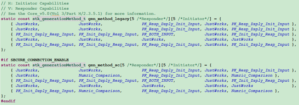
For details about the mapping relationship, please refer to “core5.0” (Vol3/Part H/2.3.5.1 Selecting Key Generation Method).
LE security mode1 level 3 supports the methods below to configure initial values:
a) Initialization setting of OOB for device with legacy pairing:
blc_smp_enableOobAuthentication(1);
blc_smp_peripheral_init(); //SMP parameter configuration must be placed before this API
Considering TK value transfer by OOB, the SDK provides related GAP event in the APP layer (see section 3.3.5.2 GAP event). The API below serves to set TK value of OOB.
void blc_smp_setTK_by_OOB (u8 *oobData);
The parameter “oobData” indicates the head pointer for the array of 16-digit TK value to be set.
b) Initialization setting of Passkey Entry (PK_Resp_Dsply_Init_Input) for device with legacy pairing:
blc_smp_enableAuthMITM(1);
blc_smp_setIoCapability(IO_CAPABILITY_DISPLAY_ONLY);
blc_smp_peripheral_init();
c) Initialization setting of Passkey Entry (PK_Init_Dsply_Resp_Input or PK_BOTH_INPUT) for device with legacy pairing:
blc_smp_enableAuthMITM(1);
blc_smp_setIoCapability(IO_CAPABLITY_KEYBOARD_ONLY);
blc_smp_peripheral_init();
Considering TK value input by user, the SDK provides related GAP event in the APP layer (see section 3.3.5.2 GAP event). The API below serves to set TK value of Passkey Entry:
void blc_smp_setTK_by_PasskeyEntry (u32 pinCodeInput);
The parameter “pinCodeInput” indicates the pincode value to be set and its range is 0~999999. It applies to the case of Passkey Entry method in which Master displays TK and Slave needs to input TK.
The KEY generation method finally adopted is related to SMP security level supported by two pairing sides. If Master only supports LE security mode1 level1, since Master does not support pairing encryption, Slave won’t enable SMP function.
(4) LE security mode1 level4
Level 4 indicates device supports the highest security level “Authenticated LE Secure Connections”, e.g. Numeric Comparison/Passkey Entry/Out of Band in secure connection pairing mode.
LE security mode1 level4 supports the methods below to configure initial values:
a) Initialization setting of Numeric Comparison for device with secure connection pairing:
blc_smp_setParingMethods(LE_Secure_Connection);
blc_smp_enableAuthMITM(1);
blc_smp_setIoCapability(IO_CAPABLITY_DISPLAY_YESNO);
Considering display of numerical comparison result to user, the SDK provides related GAP event in the APP layer (see section 3.3.5.2 GAP event).The API below serves to set numerical comparison result as “YES” or “NO”.
void blc_smp_setNumericComparisonResult(bool YES_or_NO);
The parameter “YES_or_NO” serves to confirm whether six-digit values on two sides are consistent. If yes, input 1 to indicate “YES”; otherwise input 0 to indicate “NO”.
b) Initialization setting of Passkey Entry for device with secure connection pairing:
User initialization code of this part is almost the same with that of the configuration mode B/C (Passkey Entry in legacy pairing) in LE security mode1 level3, except that pairing method herein should be set as “secure connection pairing” at the start of initialization.
blc_smp_setParingMethods(LE_Secure_Connection);
.....//Refer to configuration method B/C in LE security mode1 level3
c) Initialization setting of Out of Band for device with secure connection pairing:
This part is not implemented in current SDK yet.
(5) Several APIs related to SMP parameter configuration:
a) The API below serves to set whether to enable bonding function:
void blc_smp_setBondingMode(bonding_mode_t mode);
Following shows the enum type bonding_mode_t:
typedef enum {
    Non_Bondable_Mode = 0,
    Bondable_Mode     = 1,
}bonding_mode_t;
For device with security level other than mode1 level1, bonding function must be enabled. Since the SDK has enabled bonding function by default, generally user does not need to invoke this API.
b) The API below serves to set whether to enable Key Press function:
void blc_smp_enableKeypress (int keyPress_en);
It indicates whether it’s supported to provide some necessary input status information for KeyboardOnly device during Passkey Entry. Since the current SDK does not support this function yet, the parameter must be set as 0.
c) The API below serves to set whether to enable key pairs for ECDH (Elliptic Curve Diffie-Hellman) debug mode:
void blc_smp_setEcdhDebugMode(ecdh_keys_mode_t mode);
Following shows the definition for the enum type ecdh_keys_mode_t:
typedef enum {
    non_debug_mode = 0,//ECDH distribute private/public key pairs
    debug_mode = 1,//ECDH use debug mode private/public key pairs
} ecdh_keys_mode_t;
This API only applies to the case with secure connection pairing. The ellipse encryption algorithm can prevent eavesdropping effectively, but at the same time, it’s not very friendly to debugging and development, since user cannot capture BLE packet in the air by sniffer and analyze the data. Thus, as defined in BLE spec, ellipse encryption mode with private and public key pairs is provided for debugging. As long as this mode is enabled, BLE sniffer tool can use the known key to decrypt the link.
d) Following is a unified API to set whether to enable bonding, whether to enable MITM flag, whether to support OOB, whether to support Keypress notification, as well as to set supported IO capability(The previous documents are all separate configuration APIs. For the convenience of user settings, the SDK also provides a unified configuration API).
void blc_smp_setSecurityParameters (bonding_mode_t mode,int MITM_en,int OOB_en, int keyPress_en,
io_capability_t ioCapablility);
Definition for each parameter herein is consistent with the same parameter in the corresponding independent API.
Security Request Configuration
Only Slave can send SMP Security Request, so this part only applies to Slave device.
During phase 1 of pairing process, there’s an optional Security Request packet which serves to enable Slave to actively trigger pairing process to start. The SDK provides the API below to flexibly set whether Slave sends Security Request to Master immediately after connection/re-connection, or delay for pending_ms miliseconds before sending Security Request, or does not send Security Request, so as to implement different pairing trigger combination.
blc_smp_configSecurityRequestSending( secReq_cfg newConn_cfg, secReq_cfg reConn_cfg, u16 pending_ms);
Following shows the definition for the enum type secReq_cfg:
typedef enum {
    SecReq_NOT_SEND = 0,
    SecReq_IMM_SEND = BIT(0),
    SecReq_PEND_SEND = BIT(1),
}secReq_cfg;
The meaning of each parameter is introduced as below:
-
SecReq_NOT_SEND: After connection is established, Slave won’t send Security Request actively.
-
SecReq_IMM_SEND: After connection is established, Slave will send Security Request immediately.
-
SecReq_PEND_SEND: After connection is established, Slave will wait for pending_ms miliseconds and then determine whether to send Security Request.
(1) For the first connection, Slave receives Pairing_request from Master before pending_ms miliseconds, and it won’t send Security Request;
(2) For re-connection, if Master has already sent LL_ENC_REQ before pending_ms miliseconds to encrypt reconnection link, Slave won’t send Security Request.
The parameter “newConn_cfg” serves to configure new device, while the parameter “reConn_cfg” serves to configure device to be reconnected. During reconnection, the SDK also supports the configuration whether to send purpose of pairing request: During reconnection for a bonded device, Master may not actively initiate LL_ENC_REQ to encrypt link, and Security Request sent by Slave will trigger Master to actively enrypt the link. Therefore, the SDK provides reConn_cfg configuration, and user can configure it as needed.
Note:
This API must be invoked before connection. It’s recommended to invoke it during initialization.
The input parameters for the API “blc_smp_configSecurityRequestSending” supports the nine combinations below:
| Parameter | SecReq_NOT_SEND | SecReq_IMM_SEND | SecReq_PEND_SEND |
|---|---|---|---|
| SecReq_ NOT_SEND | Not send SecReq after the first connection or reconnection (the para pending_ms is invalid). |
Not send ecReq after the first connection, and immediately send SecReq after reconnection (the para pending_ms is invalid). |
Not send ecReq after the first connection, and wait for pending_ms miliseconds to send SecReq after reconnection. (*See previous parameter description) |
| SecReq_ IMM_SEND | Immediately send SecReq after the first connection, and not send SecReq after reconnection (the para pending_ms is invalid). |
Immediately send SecReq after the first connection or reconnection (the para pending_ms is invalid). |
Immediately send SecReq after the first connection, and wait for pending_ms miliseconds to send SecReq after reconnection. (*See previous parameter description) |
| SecReq_ PEND_SEND | Wait for pending_ms miliseconds to send SecReq after the first connection (*See previous parameter description), and not send SecReq after reconnection. |
Wait for pending_ms miliseconds to send SecReq after the first connection (*See previous parameter description), and immediately send SecReq after reconnection. |
Wait for pending_ms miliseconds to send SecReq after the first connection or reconnection. (*See previous parameter description) |
Following shows two examples:
(1) newConn_cfg: SecReq_NOT_SEND
reConn_cfg: SecReq_NOT_SEND
pending_ms: This parameter does not take effect.
When newConn_cfg is set as SecReq_NOT_SEND, it means new Slave device won’t actively initiate Security Request, and it will only respond to the pairing request from the peer device. If the peer device does not send pairing request, encryption pairing won’t be executed. As shown in the figure below, when Master sends a pairing request packet “SM_Pairing_Req”, Slave will respond to it, but won’t actively trigger Master to initiate pairing request.

When reConn_cfg is set as SecReq_NOT_SEND, it means device pairing has already been completed, and Slave won’t send Security Reqeust after reconnection.
(2) newConn_cfg: SecReq_IMM_SEND
reConn_cfg: SecReq_NOT_SEND
pending_ms: This parameter does not take effect.
When newConn_cfg is set as SecReq_IMM_SEND, it means new Slave device will immediately send Security Request to Master after connection, to trigger Master to start pairing process. As shown in the figure below, Slave actively sends a SM_Security_Req to trigger Master to send pairing request.

When reConn_cfg is set as SecReq_NOT_SEND, it means Slave won’t send Security Reqeust after reconnection.
The SDK also provides an API to send Security Request packet only for special use case. The APP layer can invoke this API to send Security Request at any time.
int blc_smp_sendSecurityRequest (void);
Note: If user invokes the “blc_smp_configSecurityRequestSending” to control secure pairing request packet, the “blc_smp_sendSecurityRequest” should not be invoked.
SMP Bonding info
SMP bonding information herein is discussed relative to Slave device. User can refer to the code of "direct advertising" setting during initialization in the SDK demo "8208_ble_sample".
Slave can store pairing information of up to four Master devices at the same time, so that all of the four devices can be reconnected successfully. The API below serves to set the max number of bonding devices with the upper limit of 4 which is also the default value.
#define         SMP_BONDING_DEVICE_MAX_NUM                  4
ble_sts_t blc_smp_param_setBondingDeviceMaxNumber( int device_num);
If using blc_smp_param_setBondingDeviceMaxNumber (4) to set the max number as 4, after four devices have been paired, excuting pairing for the fifth device will automatically delete the pairing info of the earliest connected (first) device, so as to store the pairing info of the fifth device.
If using blc_smp_param_setBondingDeviceMaxNumber (2) to set the max number as 2, after two devices have been paired, excuting pairing for the third device will automatically delete the pairing info of the earliest connected (first) device, so as to store the pairing info of the third device.
The API below serves to obtain the number of currently bonded Master devices (successfully paired with Slave) stored in the flash.
u8 blc_smp_param_getCurrentBondingDeviceNumber(void);
Assuming a return value of 3, this means that there are currently 3 successfully paired devices stored on the flash, and that all 3 devices can be connected back successfully.
(1) Storage sequence for bonding info
Index is a concept related to BondingDeviceNumber. If current BondingDeviceNumber is 1, there’s only one bonding device whose index is 0; if BondingDeviceNumber is 2, there’re two bonding devices with index 0 and 1.
The SDK provides two methods to update device index, Index_Update_by_Connect_Order and Index_Update_by_Pairing_Order, i.e. update index as per the time sequence of lastest connection or pairing for devices. The API below serves to select index update method.
void bls_smp_setIndexUpdateMethod(index_updateMethod_t method);
Following shows the enum type index_updateMethod_t:
typedef enum {
    Index_Update_by_Pairing_Order = 0,     //default value
    Index_Update_by_Connect_Order = 1,
} index_updateMethod_t;
Two index update methods are introduced below:
a) Index_Update_by_Connect_Order
If BondingDeviceNumber is 2, device index stored in Slave flash includes 0 and 1. Index sequence is updated by the order of the latest successful connection rather than the latest pairing. Suppose Slave is paired with MasterA and MasterB in sequence, since MasterB is the latest connected device, the index for MasterA is 0, while the index for MasterB is 1. Then reconnect Slave with MasterA. Now MasterA becomes the latest connected device, so the index for MasterB is 0, and the index for MasterA is 1.
If BondingDeviceNumber is 3, device index includes 0, 1 and 2. The index for the latest connected device is 2, and index for the earliest connected device is 0.
If BondingDeviceNumber is 4, device index includes 0, 1, 2 and 3. The index for the latest connected device is 3, and index for the earliest connected device is 0. Suppose Slave is paired with MasterA, MasterB, MasterC and MasterD in sequence, the index for the latest connected MasterD is 3. If Slave is reconnected with MasterB, the index for the latest connected MasterB is 3.
Since the upper limit for bonding devices is 4, please note the case when more than four Master devices are paired: When Slave is paired with MasterA, MasterB, MasterC and MasterD in sequence, pairing Slave with MasterE will make Slave delete the pairing info for MasterA; however, if Slave is reconnected with MasterA before pairing Slave with MasterE, since the sequence changes to B-C-D-A, the latest pairing operation between Slave and MasterE will delete the pairing info for MasterB.
b) Index_Update_by_Pairing_Order
If BondingDeviceNumber is 2, device index stored in Slave flash includes 0 and 1. Index sequence is updated by the order of the latest pairing. Suppose Slave is paired with MasterA and MasterB in sequence, since MasterB is the latest paired device, the index for MasterA is 0, while the index for MasterB is 1. Then reconnect Slave with MasterA. Now the index sequence for MasterA and MasterB is not changed.
If BondingDeviceNumber is 4, device index includes 0, 1, 2 and 3. The index for the latest paired device is 3, and the index for the earliest paired device is 0. Suppose Slave is paired with MasterA, MasterB, MasterC and MasterD in sequence, the index for the latest paired MasterD is 3. No matter how Slave is reconnected with MasterA/B/C/D, the index sequence won’t be changed.
Note:
When Slave is paired with MasterA, MasterB, MasterC and MasterD in sequence, pairing Slave with MasterE will make Slave delete the pairing info for MasterA; if Slave is reconnected with MasterA before pairing Slave with MasterE, since the sequence is still A-B-C-D, the latest pairing operation between Slave and MasterE will delete the pairing info for MasterA.
(2) Format for bonding info and related APIs
Bonding info of Master device is stored in flash with the format below:
typedef struct {
    u8      flag;
    u8      peer_addr_type;  //address used in link layer connection
    u8      peer_addr[6];
    u8      peer_key_size;
    u8      peer_id_adrType; //peer identity address information in key distribution, used to identify
    u8      peer_id_addr[6];
    u8      own_ltk[16];      //own_ltk[16]
    u8      peer_irk[16];
    u8      peer_csrk[16];
}smp_param_save_t;
Bonding info includes 64 bytes.
-
peer_addr_type and peer_addr indicate Master connection address in the Link Layer which is used during device direct advertising.
-
peer_id_adrType/peer_id_addr and peer_irk are identity address and irk declared in the key distribution phase.
Only when the peer_addr_type and peer_addr are Resolvable Private Address (RPA), and address filtering is needed, should related info be added into resolving list for Slave to analyze it (refer to TEST_WHITELIST in the B91_feature_test).
Other parameters are negligible to user.
The API below serves to obtain device information from flash by using index.
u32 bls_smp_param_loadByIndex(u8 index, smp_param_save_t* smp_param_load);
If the return value is 0, it indicates failure to get info; non-zero return value indicates starting flash address to store the info. For example, suppose there’re three bonded devices, get the information about the nearest connected device.
bls_smp_param_loadByIndex(2, …)
The API below serves to obtain bonding device info from flash by using Master address (connection address in the Link Layer).
u32 bls_smp_param_loadByAddr(u8 addr_type, u8* addr, smp_param_save_t* smp_param_load);
If the return value is 0, it indicates failure to get info; non-zero return value indicates starting flash address to store the info.
The API below is used for Slave device to erase all pairing info stored in local flash.
void bls_smp_eraseAllParingInformation(void);
Note: Before invoking this API, please ensure the device is in non-connection state.
The API below is used for Slave device to configure address to store pairing info in flash.
void bls_smp_configParingSecurityInfoStorageAddr(int addr);
User can set the parameter “addr” as needed, and please refer to the section 2.1.4 SDK flash space partition so as to determine a suitable flash area for bonding info storage.
SMP Failure Management
When SMP fails, a callback function can be used to control whether the connection is maintained or disconnected. This is implemented as follows.
(1) Register the handler function for the gap layer and open the event mask with the event GAP_EVT_SMP_PAIRING_FAIL , as follows.
    blc_gap_registerHostEventHandler( app_host_event_callback );
    blc_gap_setEventMask( GAP_EVT_MASK_SMP_PARING_FAIL );
(2) Modify the corresponding processing under this mask in the processing function.
int app_host_event_callback (u32 h, u8 *para, int n)
{
    u8 event = h & 0xFF;

    switch(event)
    {
        case GAP_EVT_SMP_PAIRING_FAIL:
        {
            gap_smp_paringFailEvt_t* p = (gap_smp_paringFailEvt_t*)para;
            //the operation wanted
        }
        break;

        default:
        break;
    }

    return 0;
}
GAP
GAP initialization
GAP initialization for Master and Slave is different. Slave uses the API below to initialize GAP.
void blc_gap_peripheral_init(void);
The Master initialises the GAP using the following API.
void blc_gap_central_init(void);
As introduced earlier, data transfer between the APP layer and the Host is not controlled via GAP; the ATT, SMP and L2CAP can directly communicate with the APP layer via corresponding interface. In current SDK version, the GAP layer mainly serves to process events in the Host layer, and GAP initialization mainly registers processing function entry for events in the Host layer.
GAP Event
GAP event is generated during the communication process of Host protocol layers such as ATT, GATT, SMP and GAP. As introduced earlier, current SDK supports two types of event: Controller event, and GAP (Host) event. Controller event also includes two sub types: HCI event, and Telink defined event.
GAP event processing is added in current BLE SDK, which enables the protocol stack to layer events more clearly and to process event communication in the user layer more conveniently. SMP related processing, such as Passkey input and notification of pairing result to user, is also included.
If user wants to receive GAP event in the APP layer, it’s needed to register the corresponding callback function, and then enable the corresponding mask.
Following shows the prototype and register interface for callback function of GAP event.
typedef int (*gap_event_handler_t) (u32 h, u8 *para, int n);
void blc_gap_registerHostEventHandler (gap_event_handler_t  handler);
The “u32 h” in the callback function prototype is the mark of GAP event which will be frequently used in the bottom layer protocol stack.
Following lists some events which user may use.
#define GAP_EVT_SMP_PAIRING_BEGIN                                    0
#define GAP_EVT_SMP_PAIRING_SUCCESS                                  1
#define GAP_EVT_SMP_PAIRING_FAIL                                     2
#define GAP_EVT_SMP_CONN_ENCRYPTION_DONE                             3
#define GAP_EVT_SMP_SECURITY_PROCESS_DONE                            4
#define GAP_EVT_SMP_TK_DISPALY                                       8
#define GAP_EVT_SMP_TK_REQUEST_PASSKEY                               9
#define GAP_EVT_SMP_TK_REQUEST_OOB                                   10
#define GAP_EVT_SMP_TK_NUMERIC_COMPARE                               11
#define GAP_EVT_ATT_EXCHANGE_MTU                                     16
#define GAP_EVT_GATT_HANDLE_VLAUE_CONFIRM                            17
In the callback function prototype, “para” and “n” indicate data and data length of event. User can refer to the usage below in the 8208_feature/feature_gatt_security/app.c and the implementation of the function app_host_event_callback.
blc_gap_registerHostEventHandler( app_host_event_callback );
The API below serves to enable the mask for GAP event.
void blc_gap_setEventMask(u32 evtMask);
Following lists the definition for some common eventMasks. For other event masks, user can refer to the “ble/gap/gap_event.h”.
#define GAP_EVT_MASK_NONE                          0x00000000
#define GAP_EVT_MASK_SMP_PAIRING_BEGIN             (1<<GAP_EVT_SMP_PAIRING_BEGIN)
#define GAP_EVT_MASK_SMP_PAIRING_SUCCESS           (1<<GAP_EVT_SMP_PAIRING_SUCCESS)
#define GAP_EVT_MASK_SMP_PAIRING_FAIL              (1<<GAP_EVT_SMP_PAIRING_FAIL)
#define GAP_EVT_MASK_SMP_CONN_ENCRYPTION_DONE      (1<<GAP_EVT_SMP_CONN_ENCRYPTION_DONE)
#define GAP_EVT_MASK_SMP_SECURITY_PROCESS_DONE     (1<<GAP_EVT_SMP_SECURITY_PROCESS_DONE)
#define GAP_EVT_MASK_SMP_TK_DISPALY                (1<<GAP_EVT_SMP_TK_DISPALY)
#define GAP_EVT_MASK_SMP_TK_REQUEST_PASSKEY        (1<<GAP_EVT_SMP_TK_REQUEST_PASSKEY)
#define GAP_EVT_MASK_SMP_TK_REQUEST_OOB            (1<<GAP_EVT_SMP_TK_REQUEST_OOB)
#define GAP_EVT_MASK_SMP_TK_NUMERIC_COMPARE        (1<<GAP_EVT_SMP_TK_NUMERIC_COMPARE)
#define GAP_EVT_MASK_ATT_EXCHANGE_MTU              (1<<GAP_EVT_ATT_EXCHANGE_MTU)
#define GAP_EVT_MASK_GATT_HANDLE_VLAUE_CONFIRM     (1<<GAP_EVT_GATT_HANDLE_VLAUE_CONFIRM)
If user does not set GAP event mask via this API, the APP layer won’t receive notification when corresponding GAP event is generated.
Note:
For the description about GAP event below, it’s supposed that GAP event callback has been registered, and corresponding eventMask has been enabled.
(1) GAP_EVT_SMP_PAIRING_BEGIN
Event trigger condition: When entering connection state, Slave sends a SM_Security_Req command, and Master sends a SM_Pairing_Req to request for pairing. When Slave receives the pairing request, this event will be triggered to indicate that pairing starts.

Data length “n”: 4.
Pointer “p”: p points to data of a memory area, corresponding to the structure below.
typedef struct {
    u16 connHandle;
    u8  secure_conn;
    u8  tk_method;
} gap_smp_paringBeginEvt_t;
“connHandle”: current connection handle.
“secure_conn”: If it’s 1, secure encryption feature (LE Secure Connections) will be used; otherwise LE legacy pairing will be used.
“tk_method”: It indicates the method of TK value to be used in the subsequent pairing, e.g. JustWorks, PK_Init_Dsply_Resp_Input, PK_Resp_Dsply_Init_Input, Numric_Comparison.
(2) GAP_EVT_SMP_PAIRING_SUCCESS
Event trigger condition: This event will be generated when the whole pairing process is completed correctly. This phase is called “Key Distribution, Phase 3” of LE pairing phase. If there’s key to be distributed, the pairing success event will be triggered after the two sides have completed key distribution; otherwise the pairing success event will be triggered directly.
Data length “n”: 4.
Pointer “p”: p points to data of a memory area, corresponding to the structure below.
typedef struct {
    u16 connHandle;
    u8  bonding;
    u8  bonding_result;
} gap_smp_paringSuccessEvt_t;
“connHandle”: current connection handle.
“bonding”: If it’s 1, bonding function is enabled; otherwise bonding function is disabled.
“bonding_result”: It indicates bonding result. If bonding function is disabled, the result value should be 0. If bonding function is enabled, it’s also needed to check whether encryption Key is correctly stored in flash; if yes, the result value is 1; otherwise the result value is 0.
(3) GAP_EVT_SMP_PAIRING_FAIL
Event trigger condition: If Slave or Master does not conform to standard pairing flow, or pairing process is terminated due to abnormity such as error report during communication, this event will be triggered.
Data length “n”: 2.
Pointer “p”: p points to data of a memory area, corresponding to the structure below.
typedef struct {
    u16 connHandle;
    u8  reason;
} gap_smp_paringFailEvt_t;
“connHandle”: current connection handle.
“reason”: It indicates the reason for pairing failure. Following lists some common reason values, and for other values, please refer to the file “stack/ble/smp/smp_const.h”.
For the definition of pairing failure values, please refer to “Core_v5.0” (Vol 3/Part H/3.5.5 “Pairing Failed”).
#define PAIRING_FAIL_REASON_CONFIRM_FAILED              0x04
#define PAIRING_FAIL_REASON_PAIRING_NOT_SUPPORTED       0x05
#define PAIRING_FAIL_REASON_DHKEY_CHECK_FAIL            0x0B
#define PAIRING_FAIL_REASON_NUMUERIC_FAILED             0x0C
#define PAIRING_FAIL_REASON_PAIRING_TIEMOUT             0x80
#define PAIRING_FAIL_REASON_CONN_DISCONNECT             0x81
(4) GAP_EVT_SMP_CONN_ENCRYPTION_DONE
Event trigger condition: When Link Layer encryption is completed (the LL receives “start encryption response” from Master), this event will be triggered.
Data length “n”: 3.
Pointer “p”: p points to data of a memory area, corresponding to the structure below.
typedef struct {
    u16 connHandle;
    u8  re_connect;   //1: re_connect, encrypt with previous distributed LTK;   0: pairing , encrypt with STK
} gap_smp_connEncDoneEvt_t;
“connHandle”: current connection handle.
“re_connect”: If it’s 1, it indicates fast reconnection (The LTK distributed previously will be used to encrypt the link); if it’s 0, it indicates current encryption is the first encryption.
(5) GAP_EVT_MASK_SMP_SECURITY_PROCESS_DONE
Event trigger condition: when pairing for the first time, it is triggered after the GAP_EVT_SMP_PAIRING_SUCCESS event, and in the fast reconnection, triggered after GAP_EVT_SMP_CONN_ENCRYPTION_DONE event.
Data length “n”: 3.
Pointer “p”: p points to data of a memory area, corresponding to the structure below.
typedef struct {
    u16 connHandle;
    u8  re_connect;   //1: re_connect, encrypt with previous distributed LTK;   0: paring , encrypt with STK
} gap_smp_securityProcessDoneEvt_t;
“re_connect”: If it’s 1, it indicates fast reconnection (The LTK distributed previously will be used to encrypt the link); if it’s 0, it indicates current encryption is the first encryption.
(6) GAP_EVT_SMP_TK_DISPALY
Event trigger condition: After Slave receives a Pairing_Req from Master, as per the pairing parameter configuration of the peer device and the local device, the method of TK (pincode) value to be used for pairing will be known. If the method “PK_Resp_Dsply_Init_Input” is enabled, which means Slave displays 6-digit pincode and Master inputs 6-digit pincode, this event will be triggered.
Data length “n”: 4.
Pointer “p”: p points to an u32-type variable “tk_set”. The value is 6-digit pincode that Slave needs to inform the APP layer, and the APP layer needs to display the pincode.
The user can also manually set a user-specified pincode code such as "123456" without using the 6-digit pincode code generated by underlying layer randomly, using the following API.
If the user does not use the 6-digit pincode code randomly generated by underlying layer when debugging, he can manually set a user-specified pincode code, such as "123456", using the following API.
void blc_smp_manualSetPinCode_for_debug(u16 connHandle, u32 pinCodeInput);
User should get the 6-digit pincode from Slave and input the pincode on Master side (e.g. Mobile phone), to finish TK input and continue pairing process. If user has input wrong pincode, or has clicked “cancel”, the pairing process fails.
The demo "vendor/8208_feature/feature_gatt_security/app.c" provides an example for Passkey Entry application.
case GAP_EVT_SMP_TK_DISPALY:
{
    char pc[7];
    u32 pinCode = *(u32*)para;
    sprintf(pc, "%d", pinCode);
    printf("TK display:%s\n", pc);
}
break;
(7) GAP_EVT_SMP_TK_REQUEST_PASSKEY
Event trigger condition: When the slave device enables the Passkey Entry mode and the PK_Init_Dsply_Resp_Input or PK_BOTH_INPUT pairing mode is used, this event will be triggered to notify the user that the TK value needs to be input. After receiving the event, the user needs to input the TK value through the IO input port (if the timeout is 30s, the pairing fails). The API for inputting the TK value: blc_smp_setTK_by_PasskeyEntry is explained in the "SMP parameter configuration" chapter.
Data length “n”: 0.
Pointer “p”: NULL.
(8) GAP_EVT_SMP_TK_REQUEST_OOB
Event trigger condition: When Slave device enables the OOB method of legacy pairing, this event will be triggered to inform user that 16-digit TK value should be input by the OOB method. After this event is received, user needs to input 16-digit TK value within 30s via IO input capability, otherwise pairing will fail due to timeout. For the API “blc_smp_setTK_by_OOB” to input TK value, please refer to section 3.3.4.2 SMP parameter configuration.
Data length “n”: 0.
Pointer “p”: NULL.
(9) GAP_EVT_SMP_TK_NUMERIC_COMPARE
Event trigger condition: After Slave receives a Pairing_Req from Master, as per the pairing parameter configuration of the peer device and the local device, the method of TK (pincode) value to be used for pairing will be known. If the method “Numeric_Comparison” is enabled, this event will be triggered immediately. For “Numeric_Comparison”, a method of SMP4.2 secure encryption, dialog window will pop up on both Master and Slave to show 6-digit pincode, “YES” and “NO”; user needs to check whether pincodes on the two sides are consistent, and decide whether to click “YES” to confirm TK check result is OK.
Data length “n”: 4.
Pointer “p”: p points to an u32-type variable “pinCode”. The value is 6-digit pincode that Slave needs to inform the APP layer. The APP layer needs to display the pincode, and supplies “YES or “NO” confirmation mechanism.
The demo "vendor/8208_feature/feature_gatt_security/app.c" provides an example for Numeric_Comparison application.
(10) GAP_EVT_ATT_EXCHANGE_MTU
Event trigger condition: This event will be triggered in either of the two cases below.
- Master sends “Exchange MTU Request”, and Slave responds with “Exchange MTU Response”.
- Slave sends “Exchange MTU Request”, and Master responds with “Exchange MTU Response”.
Data length “n”: 6.
Pointer “p”: p points to data of a memory area, corresponding to the structure below.
typedef struct {
    u16 connHandle;
    u16 peer_MTU;
    u16 effective_MTU;
} gap_gatt_mtuSizeExchangeEvt_t;
connHandle: current connection handle.
peer_MTU: RX MTU value of the peer device.
effective_MTU = min(CleintRxMTU, ServerRxMTU). “CleintRxMTU” and “ServerRxMTU” indicate RX MTU size value of Client and Server respectively. After Master and Slave exchanges MTU size of each other, the minimum of the two values is used as the maximum MTU size value for mutual communication between them.
(11) GAP_EVT_GATT_HANDLE_VLAUE_CONFIRM
Event trigger condition: Whenever the APP layer invokes the “blc_gatt_pushHandleValueIndicate” to send indicate data to Master, Master will respond with a confirmation for the data. This event will be triggered when Slave receives the confirmation.
Data length “n”: 0.
Pointer “p”: Null pointer.
Low Power Management
Low Power Management is also called Power Management, or PM as referred by this document.
Low Power Driver
Low Power Mode
The 8208 MCU is in working mode when executing the program normally, and the working current is between 3~7mA. To save power consumption, MCU should enter low power mode.
There are three low power modes, or sleep modes: suspend mode, deepsleep mode, and deepsleep retention mode.
| Module | suspend | deepsleep retention | deepsleep |
|---|---|---|---|
| Sram | 100% keep | 100% keep | 100% lost |
| digital register | 99% keep | 100% lost | 100% lost |
| analog register | 100% keep | 99% lost | 99% lost |
The table above illustrates statistically data retention and loss for SRAM, digital registers and analog registers during each sleep mode.
(1) Suspend mode (sleep mode 1)
In this mode, program execution pauses, most hardware modules of MCU are powered off, and the PM module still works normally. In this mode, IC current is about 60~70uA. Program execution continues after wakeup from suspend mode.
In suspend mode, data of the SRAM and all analog registers are maintained. In order to reduce power consumption, the SDK has set the power-down mode for some modules when entering the suspend low-power processing, at which time the digital register of the module will also be powered down, and must be re-initialized and configured after waking up. Involving:
a) A small number of digital registers in the baseband circuit. User should pay close attenton to the registers configured by the API “rf_set_power_level_index”. This API needs to be invoked after each wakeup from suspend mode.
b) The digital register that controls the state of the Dfifo. Corresponding to the related APIs in drivers/dfifo.h. When using these APIs, the user must ensure that they are reset after each suspend wake_up.
(2) Deepsleep mode (sleep mode 2)
In this mode, program execution pauses, vast majority of hardware modules are powered off, and the PM module still works. In this mode, IC current is less than 1uA, but if flash standby current comes up at 1uA or so, total current may reach 1~2uA. After wakeup from deepsleep mode, similar to power on reset, MCU will restart, and program will reboot and re-initialize.
In deepsleep mode, except a few retention analog registers, data of all registers (analog & digital) and SRAM are lost.
(3) Deepsleep retention mode (sleep mode 3)
In deepsleep mode, the current is very low, but cannot store SRAM data; while in suspend mode, though SRAM and most registers are non-volatile, but the current is high.
In order to realize some application scenarios that require low current during sleep and can ensure that the state can be restored immediately after sleep wakes up (e.g. maintain BLE connection during long sleep), a sleep mode 3 is added: deepsleep with Sram retention mode, referred to as deepsleep retention (or deep retention).
The deepsleep retention mode is also a kind of deepsleep. Most of the hardware modules of the MCU are powered off, and the PM hardware modules remain working. Power consumption is the power consumed by retention Sram plus that of deepsleep mode, and the current is about 2uA. When deepsleep mode wake up, the MCU will restart and the program will restart to initialize.
The deepsleep retention mode and deepsleep mode are consistent in register state, almost all of them are powered off. Compare with deepsleep mode, deepsleep retention mode can keep sram without power down.
In deepsleep mode and deepsleep retention mode, there are very few analog registers that can be kept without power-down. These non-power-down analog registers include:
a) Analog registers to control GPIO pull-up/down resistance
When configured via the API “gpio_setup_up_down_resistor” or the following method in the app_config.h, GPIO pull-up/down resistance are non-volatile:
#define PULL_WAKEUP_SRC_PD5 PM_PIN_PULLDOWN_100K
Please refer to the introduction of the GPIO module. Using GPIO output belongs to the state controlled by the digital register. 8208 can use GPIO output to control some peripherals during suspend, but after being switched to deepsleep retention mode, the GPIO output status becomes invalid and it cannot accurately control peripherals during sleep. At this point, you can use GPIO to simulate the state of the pull-up and pull-down resistors instead: pull-up 10K ohm instead of GPIO output high, and pull-down 100K ohm instead of GPIO output low.
b) Special retention analog registers of the PM module:
The code below shows the DEEP_ANA_REG in the drivers/lib/include/pm.h.
#define DEEP_ANA_REG0                       0x3a //initial value =0x00
#define DEEP_ANA_REG1                       0x3b //initial value =0x00,system used, user can not use
#define DEEP_ANA_REG2                       0x3c //initial value =0x0f
Please note that customers are not allowed to use ana_3b. This analog register is reserved for the underlying stack. If the application layer code uses this register, it needs to be modified. Because the number of non-power-off analog registers is relatively small, it is recommended that customers use each of its bits to indicate different status bits.
The following groups of non-drop analog registers may lose information due to wrong GPIO wakeup. For example, GPIO_PAD wakes up deepsleep at high level, but gpio is already at high level before calling cpu_sleep_wakeup function. It will cause wrong GPIO wakeup, then these analog register values will be lost.
#define DEEP_ANA_REG6                       0x35 //initial value =0x20
#define DEEP_ANA_REG7                       0x36 //initial value =0x00
#define DEEP_ANA_REG8                       0x37 //initial value =0x00
#define DEEP_ANA_REG9                       0x38 //initial value =0x00
#define DEEP_ANA_REG10                      0x39 //initial value =0xff
The user can save some important information in these analog regsiter and read the previously stored values after deepsleep/deepsleep retention wake_up.
Low Power Wake-up Source
The low-power wake-up source diagram of 8208 MCU is shown below, suspend/deepsleep/deepsleep retention can all be awakened by GPIO PAD and timer. In the BLE SDK, only two types of wake-up sources are concerned, as shown below (note that the two definitions of PM_TIM_RECOVER_START and PM_TIM_RECOVER_END in the code are not wake-up sources):
typedef enum {
     //available wake-up source for customer
     PM_WAKEUP_PAD              = BIT(0),
     PM_WAKEUP_TIMER            = BIT(2),
}SleepWakeupSrc_TypeDef;
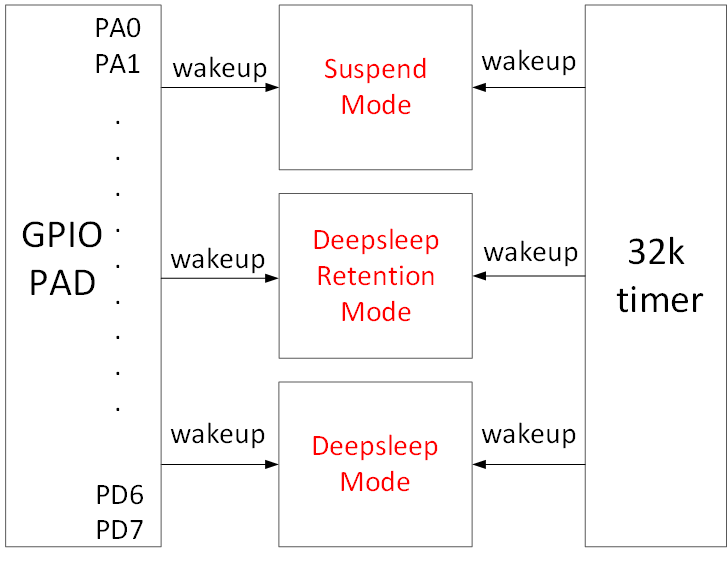
As shown above, there are two hardware wakeup sources: TIMER and GPIO PAD.
-
The PM_WAKEUP_TIMER comes from 32k HW timer (32k RC timer or 32k Crystal timer). Since 32k timer is correctly initialized in the SDK, no configuration is needed except setting wakeup source in the "cpu_sleep_wakeup ()".
-
The PM_WAKEUP_PAD comes from GPIO module. Except MSPI, all GPIOs support high or low level wakeup.
The API below serves to configure GPIO PAD as wakeup source for sleep mode.
typedef enum{
    Level_Low=0,
    Level_High =1,
} GPIO_LevelTypeDef;
void cpu_set_gpio_wakeup (GPIO_PinTypeDef pin, GPIO_LevelTypeDef pol, int en);
- “pin”: GPIO pin
- “pol”: wakeup polarity, Level_High: high level wakeup, Level_Low: low level wakeup
- “en”: 1 indicates enable, 0 indicates disable.
Examples:
cpu_set_gpio_wakeup (GPIO_PC2, Level_High, 1);  //Enable GPIO_PC2 PAD high level wakeup
cpu_set_gpio_wakeup (GPIO_PC2, Level_High, 0);  //Disable GPIO_PC2 PAD wakeup
cpu_set_gpio_wakeup (GPIO_PB5, Level_Low, 1);  //Enable GPIO_PB5 PAD low level wakeup
cpu_set_gpio_wakeup (GPIO_PB5, Level_Low, 0);  //Disable GPIO_PB5 PAD wakeup
Sleep and Wake-up From Low Power Mode
The API below serves to configure MCU sleep and wakeup.
int cpu_sleep_wakeup (SleepMode_TypeDef sleep_mode, SleepWakeupSrc_TypeDef wakeup_src,
unsigned int wakeup_tick);
- sleep_mode: This parameter serves to set sleep mode as suspend mode, deepsleep mode, or deepsleep retention 16K Sram.
typedef enum {
        SUSPEND_MODE                        = 0x00,
        DEEPSLEEP_MODE                      = 0x30,
        DEEPSLEEP_MODE_RET_SRAM_LOW16K      = 0x01,
}SleepMode_TypeDef;
-
wakeup_src: This parameter serves to set wakeup source for suspend/deep retention/deepsleep as one or combination of PM_WAKEUP_PAD and PM_WAKEUP_TIMER. If set as 0, MCU wakeup is disabled for sleep mode.
-
“wakeup_tick”: if PM_WAKEUP_TIMER is assigned as wakeup source, the “wakeup_tick” serves to set MCU wakeup time. If PM_WAKEUP_TIMER is not assigned, this parameter is negligible.
The “wakeup_tick” is an absolute value, which equals current value of System Timer tick plus intended sleep duration. When System Timer tick reaches the time defined by the wakeup_tick, MCU wakes up from sleep mode. The value of wakeup_tick needs to be based on the current System Timer tick value, plus an absolute time converted from the time to be slept, in order to effectively control the sleep time. If the wakeup_tick is set directly without taking into account the current System Timer tick, the wake-up time point cannot be controlled.
Since the wakeup_tick is an absolute time, it follows the max range limit of 32bit System Timer tick. In current SDK, 32bit max sleep time corresponds to 7/8 of max System Timer tick. Since max System Timer tick is 268s or so, max sleep time is 268*7/8=234s, which means the “delta_Tick” below should not exceed 234s.
cpu_sleep_wakeup(SUSPEND_MODE, PM_WAKEUP_TIMER, clock_time() + delta_tick);
The return value is an ensemble of current wakeup sources. Following shows wakeup source for each bit of the return value.
enum {
     WAKEUP_STATUS_PAD              = BIT(0),
     WAKEUP_STATUS_TIMER            = BIT(2),

     STATUS_GPIO_ERR_NO_ENTER_PM    = BIT(7),
};
(1) If WAKEUP_STATUS_TIMER bit = 1, wakeup source is Timer.
(2) If WAKEUP_STATUS_PAD bit = 1, wakeup source is GPIO PAD.
(3) If both WAKEUP_STATUS_TIMER and WAKEUP_STATUS_PAD equal 1, wakeup source is Timer and GPIO PAD.
(4) STATUS_GPIO_ERR_NO_ENTER_PM is a special state indicating GPIO wakeup error. E.g. Suppose a GPIO is set as high level PAD wakeup (PM_WAKEUP_PAD). When MCU attempts to invoke the “cpu_sleep_wakeup” to enter suspend, and PM_WAKEUP_PAD wake-up source is set, MCU will fail to enter suspend and immediately exit the “cpu_sleep_wakeup” with return value STATUS_GPIO_ERR_NO_ENTER_PM.
Sleep time is typically set in the following way:
cpu_sleep_wakeup (SUSPEND_MODE , PM_WAKEUP_TIMER, clock_time() + delta_Tick);
The “delta_Tick”, a relative time (e.g. 100* CLOCK_16M_SYS_TIMER_CLK_1MS), plus “clock_time()” becomes an absolute time.
Some examples on cpu_sleep_wakeup:
cpu_sleep_wakeup (SUSPEND_MODE , PM_WAKEUP_PAD, 0);
When it’s invoked, MCU enters suspend, and wakeup source is GPIO PAD.
cpu_sleep_wakeup (SUSPEND_MODE , PM_WAKEUP_TIMER, clock_time() + 10* CLOCK_16M_SYS_TIMER_CLK_1MS;
When it’s invoked, MCU enters suspend, wakeup source is timer, and wakeup time is current time plus 10ms, so the suspend duration is 10ms.
cpu_sleep_wakeup (SUSPEND_MODE , PM_WAKEUP_PAD | PM_WAKEUP_TIMER,
clock_time() + 50* CLOCK_16M_SYS_TIMER_CLK_1MS);
When it’s invoked, MCU enters suspend, wakeup source includes timer and GPIO PAD, and timer wakeup time is current time plus 50ms.
If GPIO wakeup is triggered before 50ms expires, MCU will be woke up by GPIO PAD in advance; otherwise, MCU will be woke up by timer.
cpu_sleep_wakeup (DEEPSLEEP_MODE, PM_WAKEUP_PAD, 0);
When it’s invoked, MCU enters deepsleep, and wakeup source is GPIO PAD.
cpu_sleep_wakeup (DEEPSLEEP_MODE_RET_SRAM_LOW32K , PM_WAKEUP_TIMER, clock_time() + 8* CLOCK_16M_SYS_TIMER_CLK_1S);
When it’s invoked, MCU enters deepsleep retention 32K Sram mode, wakeup source is timer, and wakeup time is current time plus 8s.
cpu_sleep_wakeup (DEEPSLEEP_MODE_RET_SRAM_LOW32K , PM_WAKEUP_PAD | PM_WAKEUP_TIMER,clock_time() + 10* CLOCK_16M_SYS_TIMER_CLK_1S);
When it’s invoked, MCU enters deepsleep retention 32K Sram mode, wakeup source includes GPIO PAD and Timer, and timer wakeup time is current time plus 10s. If GPIO wakeup is triggered before 10s expires, MCU will be woke up by GPIO PAD in advance; otherwise, MCU will be woke up by timer.
Low Power Wake-up Procedure
When user calls the API cpu_sleep_wakeup, the MCU enters the sleep mode; when the wake-up source triggers the MCU to wake up, the MCU software operation flow is inconsistent for different sleep modes.
The following is a detailed description of the MCU operating process after the suspend, deepsleep, and deepsleep retention three sleep modes are awakened. Please refer to the figure below.
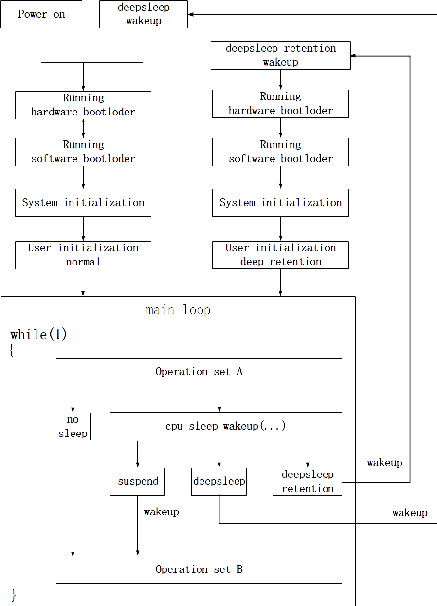
Detailed process after the MCU is powered on is introduced as following:
(1) Run hardware bootloader
It is pure MCU hardware operation without involvement of software.
Couple of examples:
Read the boot flag of flash to determine whether the firmware that should be run currently is stored on flash address 0 or on flash address 0x20000 (related to OTA); read the value of the corresponding location of flash to determine how much data currently needs to be copied from flash to Sram as resident memory data (refer to Chapter (refer to the introduction of Sram allocation in Chapter 2). The part of running the hardware bootloader involves copying data from flash to sram, which generally takes a long time to execute. For example, it takes about 5ms to copy 10K data.
(2) Run software bootloader
After hardware bootloader, MCU starts “Running software bootloader”. Software bootloader is vector side corresponding to the .s assembly program in the boot directory of the b80 sdk.
Software bootloader serves to set up memory environment for C program execution, so it can be regarded as memory initialization.
(3) System initialization
System initialization corresponds to the initialization of each hardware module (including cpu_wakeup_init, rf_drv_init, gpio_init, clock_init) from cpu_wakeup_init to user_init in the main function, and sets the digital/analog register status of each hardware module.
(4) User initialization
User initialization is divided into User initialization normal and User initialization deep retention, which correspond to the functions user_init_normal and user_init_deepRetn in the SDK respectively. For projects that do not use deep retention, such as kma master dongle, there is only user_init, which is equivalent to user_init_normal.
The user_init and user_init_normal require all the initialisation to be done, which takes longer time.
The user_init_deepRetn only needs to do some hardware related initialization, no software initialization is needed because the variables involved in software initialization are put into the MCU retention area during design time, and these variables remain unchanged during deep retention and do not need to be reset after waking up. So user_init_deepRetn is an accelerated mode, saving time and therefore power.
(5) main_loop
After User initialization, program enters main_loop inside while(1). The operation is called “Operation Set A” before main_loop enters sleep mode, and called “Operation Set B” after wakeup from sleep.
As shown in figure above, sleep mode process is detailed as following.
(6) no sleep
Without sleep mode, MCU keeps looping inside while(1) between “Operation Set A” -> “Operation Set B”.
(7) suspend
MCU enters suspend mode by invoking cpu_sleep_wakeup, wakes up from suspend after exiting from cpu_sleep_wakeup, and then executes “Operation Set B”.
Suspend can be regarded as the most “clean” sleep mode, in which data of SRAM, digital and analog registers are retained (a few special exceptions). After wakeup from suspend, program continues from the breakpoint, with almost no need to recover SRAM or registers. However, in suspend current is relatively high.
(8) deepsleep
MCU can also enter deepsleep by invoking cpu_sleep_wakeup. After wakeup from deepsleep, MCU restarts from “Running hardware bootloader”. Almost the same as power on reset, all hardware and software initialization are required after deepsleep wakeup. Since SRAM and registers - except a few retention analog registers - will lose their data in deepsleep, MCU current is decreased to less than 1uA.
(9) deepsleep retention
MCU can also enter deepsleep retention mode by invoking cpu_sleep_wakeup. After wakeup from deepsleep retention, MCU restarts from “Running software bootloader”.
The deepsleep retention is an intermediate sleep mode between suspend and deepsleep. In suspend mode, both SRAM and most registers need to retain data, which thus ends up with higher current. In deepsleep retention, it’s only needed to maintain states of a few retention analog registers, as well as data of first 16K or 32K SRAM, so current is largely decreased to 2uA or so.
After deepsleep wake_up, MCU needs to restart the whole flow. Since first 16K or 32K SRAM are non-volatile in deepsleep retention, there’s no need to re-load from flash to SRAM after wake_up, and thus “Running hardware bootloader” is skipped. Due to limited SRAM retention size, “Running software bootloader” cannot be skipped. Since deepsleep retention does not keep register state, system initialization must also be executed to re-initialize registers.
The user initialization after deepsleep retention wake_up can actually be optimized to differentiate from MCU power on and deepsleep wake_up.
API pm_is_MCU_deepRetentionWakeup
According to the figure “sleep mode wakeup work flow” above, MCU power on, deepsleep wake_up and deepsleep retention wake_up all need to go through “Running software bootloader”, “system initialization”, and “user initialization”.
While running system initialization and user initialization, user needs to know whether MCU is woke up from deepsleep retention, so as to differentiate from power on and deepsleep wake_up. The following API in the PM driver serves to make this judgement.
int pm_is_MCU_deepRetentionWakeup(void);
Return value: 1 indicates deepsleep retention wake_up; 0 indicates power on or deepsleep wake_up.
BLE Low Power Management
BLE PM Initialization
For applications with low power mode, BLE PM module needs to be initialized by following API.
void blc_ll_initPowerManagement_module(void);
If low power is not required, DO NOT use this API, so as to skip compiling of PM related code and variables into program and thus save firmware and SRAM space.
BLE PM for Link Layer
In this BLE SDK, PM module manages power consumption in BLE Link Layer. It would be helpful referring to introduction to Link Layer in earlier chapter.
The SDK has done low power management for Advertising state and Connection state Slave role, and provides a set of APIs for users to call and configure.
The SDK does not apply low power management to Idle state either. In Idle state, since there is no RF activity, i.e. the “blc_sdk_main_loop” function is not valid, user can use PM driver for certain low power management. E.g. In the demo code below, when Link Layer is in Idle state, every main_loop would suspend for 10ms.
void main_loop (void)
{
    ////////////////////// BLE entry ////////////////////////
    blc_sdk_main_loop();

    ///////////////////// UI entry //////////////////////////
    // add user task
    //////////////////// PM configuration ////////////////////////
    if(blc_ll_getCurrentState() == BLS_LINK_STATE_IDLE ){  //Idle state
        cpu_sleep_wakeup(SUSPEND_MODE, PM_WAKEUP_TIMER,
clock_time() + 10*CLOCK_16M_SYS_TIMER_CLK_1MS);
    }
    else{
        blt_pm_proc();  //BLE Adv & Conn state
    }
}
The figure below shows timing of sleep mode when Link Layer is in Advertising state or Conn state Slave role with connection latency = 0.
Note:
In the figure, Conn state Slave role is the case of connection latency = 0.
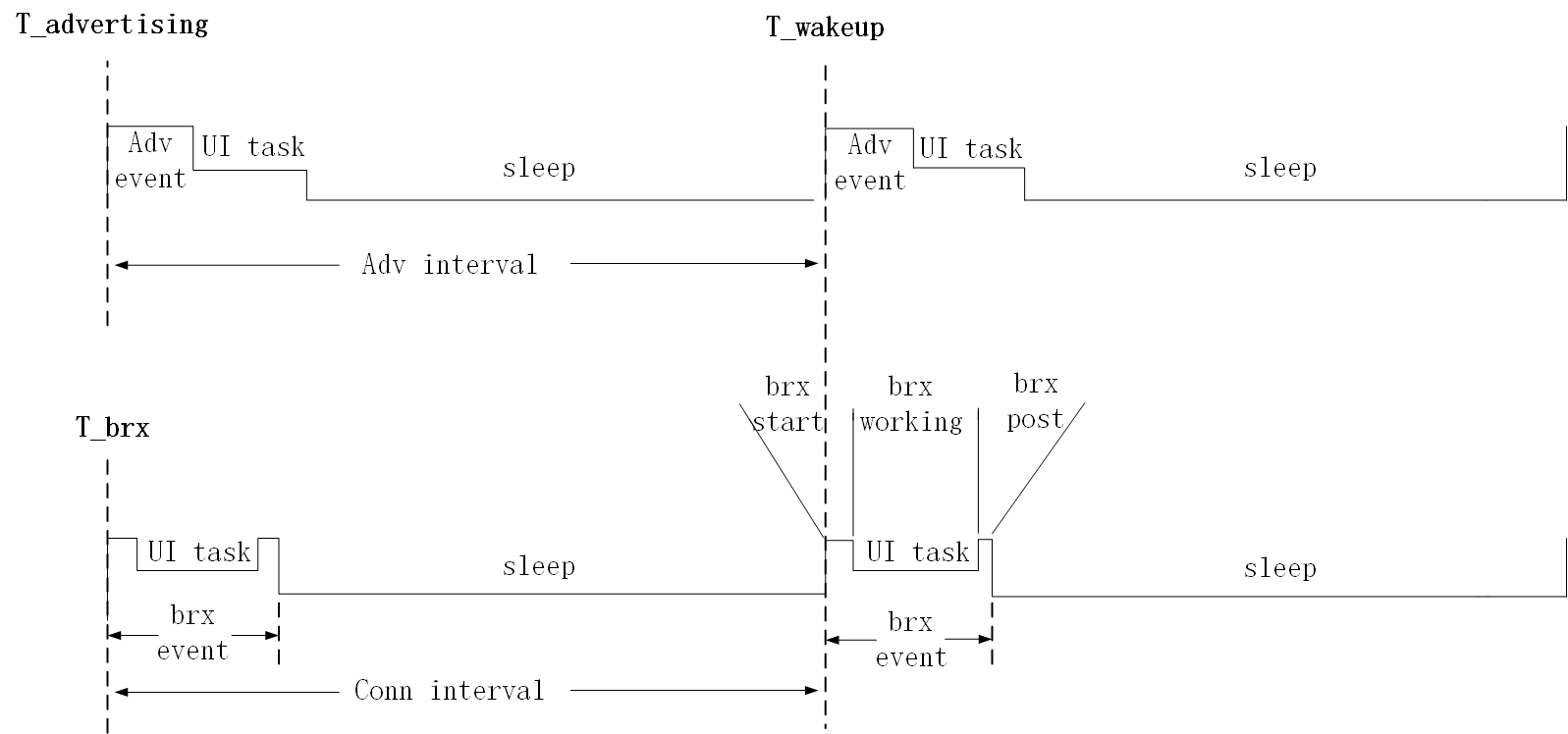
(1) In Advertising state, during each Adv Internal, Adv Event is mandatory; MCU can enter sleep mode (suspend/deepsleep retention) during the rest time other than UI task.
In figure above, the starting time of Adv event at first Adv interval is defined as T_advertising, and the time for MCU to wake up from sleep is defined as T_wakeup.T_wakeup is also the start of Adv event at next Adv interval. Both these two parameters will be elaborated in later section.
(2) During each Conn-interval at Conn state Slave role, the time for brx Event (brx start+brx working+brx post) is mandatory. MCU can enter sleep mode (suspend/ deepsleep retention) during the rest time other than UI task.
The starting time of of Brx event at first Connection interval is defined as T_brx, and the time for MCU to wake up from sleep is T_wakeup. T_wakeup is also the start of BRx event at next Connection interval. Both these two parameters will be elaborated in later section.
BLE PM is basically the sleep mode management in Advertising state or Conn state Slave role. User can select sleep mode and set related time parameters: enter sleep, enter suspend mode, or enter deepsleep retention mode.
The 8208 has 3 sleep modes: suspend, deepsleep, and deepsleep retention.
For suspend and deepsleep retention in sleep mode, the user does not need to call the API cpu_sleep_wakeup to implement. The SDK adds a low power management mechanism in BLE stack according to Link Layer state and the low power mode (the corresponding code is implemented in blc_sdk_main_loop). Users only need to call the corresponding API to configure low power consumption.
Deepsleep is not included in BLE low PM, so user needs to manually invoke the API “cpu_sleep_wakeup” in APP layer to enter deepsleep. Please refer to the “blt_pm_proc” function in the project “8208_ble_sample” of the SDK.
Following sections illustrate details of low power management in Advertising state and Connection state Slave role.
BLE PM Variables
The variables in this section are helpful to understand BLE PM software flow.
The following structures and variables are defined in the BLE SDK, and only some of the variables in the structure are listed below (variables needed to introduce the API).
typedef struct {
    u8      suspend_mask;
    u8      wakeup_src;
    u16     user_latency;
}st_ll_pm_t;

extern  u32     deepRet_advThresTick;
extern  u32     deepRet_connThresTick;
extern  u32     deepRet_earlyWakeupTick;
Following struct is defined in the file “ll_pm.c” for understanding purpose.
st_ll_pm_t bltPm;
Note:
This file is assembled in library, and user is not allowed to make any operation on this struct variable.
There will be a lot of variables like the “bltPm. suspend_mask” in later sections.
API bls_pm_setSuspendMask
The APIs below serve to configure low power management in Link Layer at “Advertising state” and “Conn state Slave role”.
void    bls_pm_setSuspendMask (u8 mask);
u8      bls_pm_getSuspendMask (void);
The “bltPm.suspend_mask” is set by the “bls_pm_setSuspendMask” and its default value is SUSPEND_DISABLE.
Following shows source code of the 2 APIs.
void  bls_pm_setSuspendMask (u8 mask)
{
        bltPm.suspend_mask = mask;
}
u8  bls_pm_getSuspendMask (void)
{
        return bltPm.suspend_mask;
}
The “bltPm.suspend_mask” can be set as any one or the “or-operation” of following values:
#define         SUSPEND_DISABLE             0
#define         SUSPEND_ADV                 BIT(0)
#define         SUSPEND_CONN                BIT(1)
#define         DEEPSLEEP_RETENTION_ADV     BIT(2)
#define         DEEPSLEEP_RETENTION_CONN    BIT(3)
The “SUSPEND_DISABLE” means sleep is disabled which allows MCU to enter neither suspend nor deepsleep retention.
The “SUSPEND_ADV” and “DEEPSLEEP_RETENTION_ADV” decide whether MCU at Advertising state can enter suspend and deepsleep retention.
The “SUSPEND_CONN” and “DEEPSLEEP_RETENTION_CONN” decide whether MCU at Conn state Slave role can enter suspend and deepsleep retention.
In low power sleep mode design of the SDK, deepsleep retention is a substitute of suspend mode to reduce sleep power consumption.
Take Conn state slave role as an example:
The SDK will first check whether SUSPEND_CONN is enabled in the “bltPm.suspend_mask”, and MCU can enter suspend only when SUSPEND_CONN is enabled. Further on, based on the value of the DEEPSLEEP_RETENTION_CONN, MCU can decide whether it will enter suspend mode or deepsleep retention mode.
Therefore, to enable MCU to enter suspend, user only needs to enable SUSPEND_ADV/SUSPEND_CONN. To enable MCU to enter deepsleep retention mode, both SUSPEND_CONN and DEEPSLEEP_RETENTION_CONN should be enabled.
Following shows 3 typical use cases:
bls_pm_setSuspendMask(SUSPEND_DISABLE);
MCU will not enter sleep mode (suspend/deepsleep retention).
bls_pm_setSuspendMask(SUSPEND_ADV | SUSPEND_CONN);
At Advertising state and Conn state Slave role, MCU can only enter suspend mode, and it’s not allowed to enter deepsleep retention.
bls_pm_setSuspendMask(SUSPEND_ADV | DEEPSLEEP_RETENTION_ADV
                    |SUSPEND_CONN | DEEPSLEEP_RETENTION_CONN);
At Advertising state and Conn state Slave role, MCU can enter both suspend and deepsleep retention, but the sleep mode to enter depends on sleeping time which will be explained later.
There may be some special applications, for example:
bls_pm_setSuspendMask(SUSPEND_ADV)
Only at Advertising state can MCU enter suspend, and at Conn state Slave role it’s not allowed to enter sleep mode.
bls_pm_setSuspendMask(SUSPEND_CONN | DEEPSLEEP_RETENTION_CONN)
Only at Conn state Slave role, can MCU enter suspend or deepsleep retention, and at Advertising state it’s not allowed to enter sleep mode.
API bls_pm_setWakeupSource
User can set the bls_pm_setSuspendMask to enable MCU to enter sleep mode (suspend or deepsleep retention), and use the following API to set wakeup source.
void bls_pm_setWakeupSource(u8 source);
“source”: Wakeup source, can be set as PM_WAKEUP_PAD.
This API sets the bottom-layer variable “bltPm.wakeup_src”. Following shows source code in the SDK.
void    bls_pm_setWakeupSource (u8 src)
{
    bltPm.wakeup_src = src;
}
When MCU enters sleep mode at Advertising state or Conn state Slave role, its actual wakeup source is:
bltPm.wakeup_src | PM_WAKEUP_TIMER
So PM_WAKEUP_TIMER is mandatory, not depending on user setup. This guarantees that MCU will wake up at specified time to handle Adv Event or Brx Event.
Everytime wakeup source is set by the “bls_pm_setWakeupSource”, after MCU wakes up from sleep mode, the bltPm.wakeup_src is set to 0.
PM software processing flow
Both actual code and pseudo-code are used herein to explain the flow details.
blc_sdk_main_loop
As shown below, the “blc_sdk_main_loop” is repetitively executed in while (1) loop of the SDK.
while(1)
{
    ////////////////////// BLE entry ////////////////////////
    blc_sdk_main_loop();
////////////////////// UI entry ////////////////////////
    //UI  task
////////////////////// user PM config ////////////////////////
    //blt_pm_proc();
}
The blc_sdk_main_loop function is executed continuously in while(1), and the code for BLE low-power management is in the blc_sdk_main_loop function, so the code for low-power management is also executed all the time.
Following shows the implementation of BLE PM logic inside the “blc_sdk_main_loop”.
int blc_sdk_main_loop (void)
{
    ……
    if(bltPm. suspend_mask == SUSPEND_DISABLE) // SUSPEND_DISABLE, can not
    {                                      // enter sleep mode
        return  0;
    }

    if( (Link Layer State == Advertising state)  ||  (Link Layer State == Conn state Slave role) )
    {
        if(Link Layer is in Adv Event or Brx Event) //RF is working, can not enter
        {                                 //sleep mode
            return  0;
        }
        else
        {
            blt_brx_sleep (); //process sleep & wakeup
        }
    }
    return 0;
}
(1) When the “bltPm.suspend_mask” is SUSPEND_DISABLE, the SW directly exits without executing the “blt_brx_sleep” function. So when using the “bls_pm_setSuspendMask(SUSPEND_DISABLE)”, PM logic is completely ineffective; MCU will never enter sleep and the SW always execute while(1) loop.
(2) When the SW is executing Adv Event at Advertising State or Brx Event at Conn state Slave role, the “blt_brx_sleep” won’t be executed either due to RF task ongoing. The SDK needs to guarantee completion of Adv Event/Brx Event before MCU enters sleep mode.
Only when both cases above are invalid, the blt_brx_sleep will be executed.
blt_brx_sleep
The logical implementation of the blt_brx_sleep function is shown below.
void    blt_brx_sleep (void)
{
    if( (Link Layer state == Adv state)&& (bltPm. suspend_mask &SUSPEND_ADV) )
    {   //current state is adv state, suspend is allowed
        T_wakeup = T_advertising + advInterval;
        “BLT_EV_FLAG_SUSPEND_ENTER” event callback execution
        T_sleep = T_wakeup – clock_time();
        if( bltPm. suspend_mask & DEEPSLEEP_RETENTION_ADV && T_sleep > bltPm.deepRet_advThresTick )
        {   //suspend is automatically switched to deepsleep retention
            cpu_sleep_wakeup (DEEPSLEEP_MODE_RET_SRAM_LOW16K, PM_WAKEUP_TIMER | bltPm.wakeup_src,T_wakeup); //suspend
            //PC value reset to 0 when MCU is woken up, will re-execute software bootloader //(cstartup_8258_16K.S), system initialization, etc.
        }
        else
        {
            cpu_sleep_wakeup (SUSPEND_MODE, PM_WAKEUP_TIMER | bltPm.wakeup_src, T_wakeup);
        }
        “BLT_EV_FLAG_SUSPEND_EXIT” event callback execution

        if(suspend is waken up by GPIO PAD)
        {
            “BLT_EV_FLAG_GPIO_EARLY_WAKEUP” event callback execution
        }
    }
    else if((Link Layer state == Conn state Slave role)&& (SuspendMask&SUSPEND_CONN) )
    {   //current Conn state, enter suspend
        if(conn_latency != 0)
        {
            latency_use = bls_calculateLatency();
            T_wakeup = T_brx + (latency_use +1) * conn_interval;
        }
        else
        {
            T_wakeup = T_brx + conn_interval;
        }
        “BLT_EV_FLAG_SUSPEND_ENTER” event callback execution
        T_sleep = T_wakeup – clock_time();
        if(  bltPm. suspend_mask & DEEPSLEEP_RETENTION_CONN &&
T_sleep  >  bltPm.deepRet_connThresTick )
        {   //suspend is automatically switched to deepsleep retention
            cpu_sleep_wakeup (DEEPSLEEP_MODE_RET_SRAM_LOW16K, PM_WAKEUP_TIMER | bltPm.wakeup_src,T_wakeup); //suspend
            //PC value reset to 0 when MCU is woken up, will re-execute software bootloader//(cstartup_8258_16K.S), system initialization, etc.
        }
        else
        {
            cpu_sleep_wakeup (SUSPEND_MODE, PM_WAKEUP_TIMER | bltPm.wakeup_src, T_wakeup);
        }

        “BLT_EV_FLAG_SUSPEND_EXIT” event callback execution
        if(suspend is waken up by GPIO PAD)
        {
            “BLT_EV_FLAG_GPIO_EARLY_WAKEUP” event callback execution
            Adjust BLE timing
        }
    }
    bltPm.wakeup_src = 0;
    bltPm.user_latency = 0xFFFF;
}
To simplify the discussion, let’s begin with an easy case: conn_latency =0, only suspend mode, no deepsleep retention. This is the case when setting suspend mask in APP layer via the “bls_pm_setSuspendMask(SUSPEND _ADV | SUSPEND_CONN)”.
Referring to controller event introduced earlier, please pay close attention to the timing of these suspend related events and callback functions: BLT_EV_FLAG_SUSPEND_ENTER, BLT_EV_FLAG_SUSPEND_EXIT, BLT_EV_FLAG_GPIO_EARLY_WAKEUP.
When Link Layer is in Advertising state with “bltPm. suspend_maskis” set to SUSPEND_ADV, or at Conn state slave role with “bltPm. suspend_mask” set to SUSPEND_CONN, MCU can enter suspend mode.
In suspend mode, the API “cpu_sleep_wakeup” in the driver is finally invoked.
cpu_sleep_wakeup (SUSPEND_MODE, PM_WAKEUP_TIMER | bltPm.wakeup_src, T_wakeup);
This API sets wakeup source as PM_WAKEUP_TIMER | bltPm.wakeup_src, so Timer wakeup is mandatory to guarantee MCU wakeup before next Adv Event or Brx Event. For wakeup time “T_wakeup”, please refer to earlier “sleep timing for Advertising state & Conn state Slave role” diagram.
When exiting the “blt_brx_sleep” function, both the “bltPm.wakeup_src” and the “bltPm.user_latency” are reset. So the API “bls_pm_setWakeupSource” and “bls_pm_setManualLatency” are only effective for current sleep mode.
Analysis of Deepsleep Retention
Introduce deepsleep retention, and continue to analyze the above software processing flow. When the application layer is set as follows, deepsleep retention mode is enabled.
bls_pm_setSuspendMask( SUSPEND_ADV | DEEPSLEEP_RETENTION_ADV | SUSPEND_CONN | DEEPSLEEP_RETENTION_CONN);
API blc_pm_setDeepsleepRetentionThreshold
At Advertising state and Conn state slave role, suspend can switch to deep retention only when following conditions are met, respectively:
if(  bltPm. suspend_mask & DEEPSLEEP_RETENTION_ADV &&T_sleep  > bltPm.deepRet_advThresTick )
if(  bltPm. suspend_mask & DEEPSLEEP_RETENTION_CONN &&T_sleep  >  bltPm.deepRet_connThresTick )
Firstly, the “bltPm. suspend_mask” should be set to DEEPSLEEP_RETENTION_ADV or DEEPSLEEP_RETENTION _CONN, as explained before.
Secondly, for T_sleep > bltPm.deepRet_advThresTick or T_sleep > bltPm.deepRet_connThresTick ,T_sleep, sleep duration time, equals Wakeup time “T_wakeup” minus current time “clock_time()”. It means that sleep duration should exceed certain threshold so that MCU can switch sleep mode from suspend to deepsleep retention.
Here is the API to set the two threshold in unit of ms for Advertising state and Conn state slave role.
void blc_pm_setDeepsleepRetentionThreshold( u32 adv_thres_ms,
u32 conn_thres_ms)
{
 bltPm.deepRet_advThresTick = adv_thres_ms * CLOCK_16M_SYS_TIMER_CLK_1MS;
 bltPm.deepRet_connThresTick = conn_thres_ms * CLOCK_16M_SYS_TIMER_CLK_1MS;
}
API blc_pm_setDeepsleepRetentionThreshold is used to set the time threshold when suspend is switched to deepsleep retention trigger condition. This design is to pursue lower power consumption.
Refer to the description of the "Run Process After Sleep Wake_up" section above. After suspend mode wake_up, you can immediately return to the environment before suspend to continue running. In the above software flow, after T_wakeup wakes up, it can immediately start executing the Adv Event/Brx Event task.
After deepsleep retention wake_up, you need to return to the place where "Run software bootloader" started. Compared with suspend wake_up, you need to run 3 more steps (Run software bootloader + System initialization + User initialization) before you can return to main_loop to execute Adv Event again. /Brx Event task.
Taking Conn state slave role as an example, the following figure shows the timing (sequence) & power (power consumption) comparison when sleep mode is suspend and deepsleepretention respectively.
The time difference T_cycle between two adjacent Brx events is the current time period. Average the power consumption of Brx Event, the equivalent current is I_brx, and the duration is t_brx (the name t_brx here is to distinguish it from the previous concept T_brx). The bottom current of Suspend is I_suspend, and the bottom current of deep retention is I_deepRet.
The average current in the process of "Run software bootloader + System initialization + User initialization" is equivalent to I_init, and the total duration is T_init. In actual applications, the value of T_init needs to be controlled and measured by the user, and how to implement it will be introduced later.
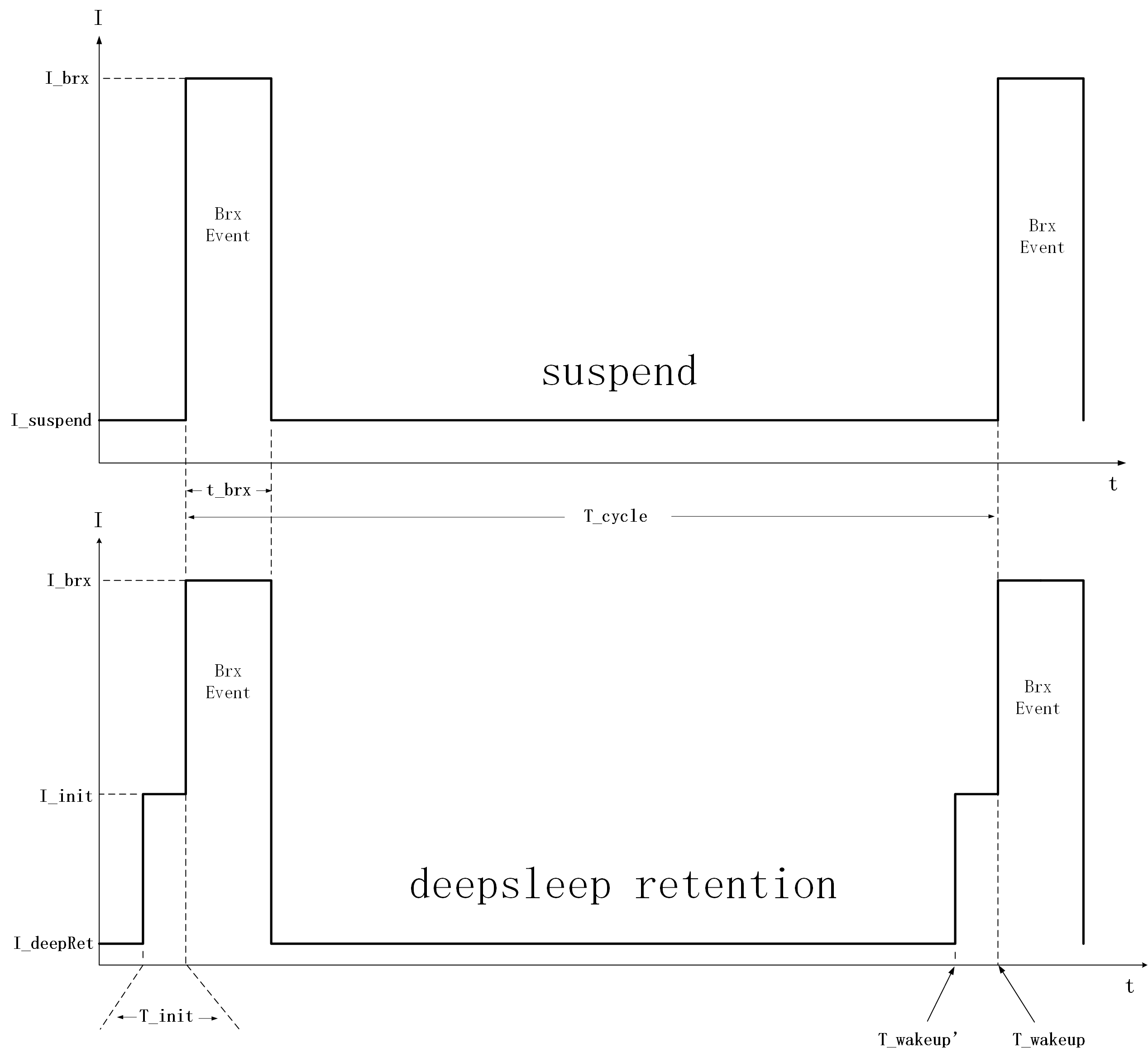
The following is the description of terms in the figure.
-
T_cycle: the time difference between two adjacent Brx events
-
I_brx: average the power consumption of Brx Event, the equivalent current is I_brx
-
t_brx: l_brx duration
-
l_suspend: suspend bottom current
-
l_deepRet: bottom current of deep retention
-
l_init: Software bootloader + System initialization + User initialization process equivalent average current
-
T_init: the total duration of l_init
Average Brx current with suspend mode is:
I_avgSuspend = I_brx*t_brx + I_suspend* (T_cycle – t_brx)
Simplified by T_cycle >> t_brx, (T_cycle – t_brx) can be regarded as T_cycle.
I_avgSuspend = I_brx*t_brx + I_suspend* T_cycle
Average Brx current with deepsleep retention mode is:
I_avgDeepRet = I_brx*t_brx + I_init*T_init + I_deepRet* (T_cycle – t_brx)
= I_brx*t_brx + I_init*T_init + I_ deepRet * T_cycle
Comparing I_avgSuspend and I_avgDeepRet, removing the same "I_brx*t_brx", the final part of the comparison is
I_avgSuspend – I_avgDeepRet = I_suspend* T_cycle – I_init*T_init – I_ deepRet * T_cycle
= T_cycle( (I_suspend – I_ deepRet) – (T_init*I_init)/T_cycle)
For application program with correct power debugging on both HW circuit and SW, the “(I_suspend - I_ deepRet)” and “(T_init*I_init)” can be regarded as fixed value.
Suppose I_suspend=30uA, I_deepRet=2uA, (I_suspend - I_ deepRet) = 28uA; I_init=3mA, T_init=400 us, (T_init*I_init)=1200 uA*us:
I_avgSuspend – I_avgDeepRet = Tcycle (28 – 1200/Tcycle)
I_avgSuspend – I_avgDeepRet
>0 when Tcycle > (1200/28) = 43ms, DeepRet consumes less power;
<0 when Tcycle < 43ms, Suspend mode consumes less power.
Mathematically, when Tcycle < 43 ms, suspend mode is more power efficient; when Tcycle > 43 ms, deepsleep retention mode is a better choice.
Note:
As you can see in the PM software processing flow section, the suspend is automatically switched to deepsleep retention only when T_sleep > 43ms. We generally consider the MCU working time (Brx Event + UI task) to be relatively short, and when T_cycle is large, we can consider T_sleep to be approximately equal to T_cycle.
By using the threshold setting API below, MCU will automatically switch suspend to deepsleep retention for T_sleep more than 43mS, and maintain suspend for T_sleep less than 43mS.
blc_pm_setDeepsleepRetentionThreshold(43, 43);
Take a long connection of 10ms connection interval * (99 + 1) = 1s as an example:
During the Conn state slave role, due to the tasks of the application layer, manual latency settings, etc., it may lead to time values such as 10ms, 20ms, 50ms, 100ms, 1s, etc. when the MCU suspend. According to the 43ms threshold setting, the MCU will automatically switch the 50ms, 100ms, 1s etc. suspend to deepsleep retention, while the 10ms, 20ms etc. suspend will still maintain suspend, such processing can ensure an optimal power consumption.
Since the power consumption of deepsleep retention is lower than that of suspend, and the presence of the 3 steps "Run software bootloader + System initialization + User initialization" results in some additional power consumption. Based on the above analysis, it must be the case that deepsleep retention will be more power efficient when T_cycle is greater than a certain threshold. The values in the above example are just a simple demo, the user needs to measure the corresponding values in the above equation according to certain methods when implementing power optimisation, and only then can the threshold value be determined.
In practice, following demos in the SDK, as long as user initialization does not incorrectly run across extended time, for T_cycle larger than 100ms, deepsleep retention mode should end up with lower power in most application scenarios.
blc_pm_setDeepsleepRetentionEarlyWakeupTiming
According to the “suspend & deepsleep retention timing & power”, suspend wake_up time “T_wakeup” is exactly the starting point of next Brx Event, or the time point when BLE master starts sending packet.
For deepsleep retention, wake_up time needs to start earlier than T_wakeup to allow T_init: running software bootloader + system initialization + user initialization, or it will miss Brx Event, i.e., the time when BLE master starts sending packet. So MCU wake_up time should be pulled in to T_wakeup’:
T_wakeup’ = T_wakeup – T_init
When applying to:
cpu_sleep_wakeup (DEEPSLEEP_MODE_RET_SRAM_LOW32K, PM_WAKEUP_TIMER | bltPm.wakeup_src,
T_wakeup - bltPm.deepRet_earlyWakeupTick);
The T_wakeup is automatically calculated by the BLE stack, while the “bltPm.deepRet_earlyWakeupTick” can be assigned to the measured T_init (or slightly larger) by following API:
void blc_pm_setDeepsleepRetentionEarlyWakeupTiming(u32 earlyWakeup_us)
{
    bltPm.deepRet_earlyWakeupTick = earlyWakeup_us *    CLOCK_16M_SYS_TIMER_CLK_1US;
}
User can directly set the measured value of T_init to the above API, or set a value slightly larger than T_init, but not less than this value.
Optimization and Measurement of T_init
For SRAM concept to be discussed in this section such as ram_code, retention_data, deepsleep retention area, please refer to section 2.1.2 SRAM space partition.
(1) T_init timing
From the figure "suspend & deepsleep retention timing & power", combined with the previous analysis, we can see that for the larger T_cycle, the sleep mode uses deepsleep retention with lower power consumption, but in this mode the T_init time is mandatory. In order to minimize the power consumption of long sleep, the time of T_init needs to be optimized to the minimum. The value of I_init is basically stable and does not need to be optimized.
The T_init is the sum of the time consumed by the 3 steps of Run software bootloader + System initialization + User initialization. The 3 steps are disassembled and analyzed, and the time of each step is defined first.
-
T_cstatup is the time of running software bootloader, i.e. executing assembly file cstartup_xxx.S.
-
T_sysInit is system initialization time.
-
T_userInit is user initialization time.
T_init = T_cstatup + T_sysInit + T_userInit
Following is a complete timing diagram of T_init:
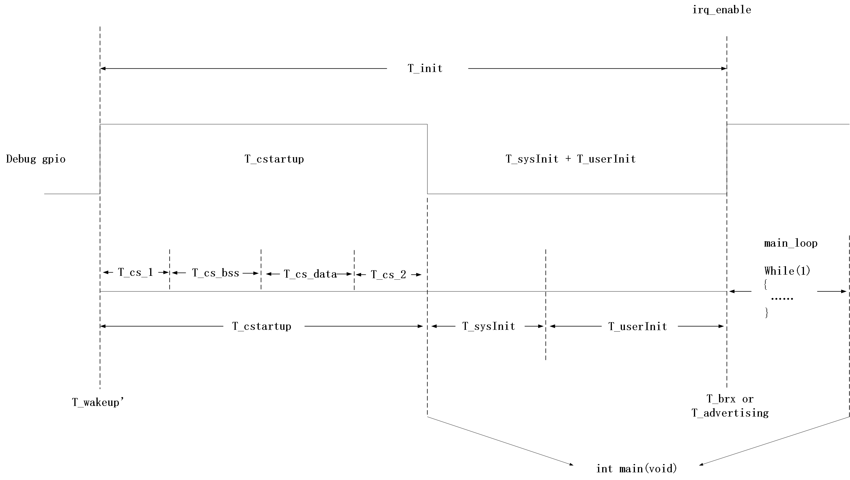
Based on earlier definition, T_wakeup is the starting point of next Adv Event/Brx Event, and T_wakeup’ is MCU early wake_uptime.
After wake_up, MCU will execute cstatup_xxx.S, jump to main() to start system initialization followed by user initialization, and then enter main_loop. Once getting in main_loop, it can start processing of Adv Event/Brx Event. The end of T_userInit is the starting point of Adv Event/Brx Event, or T_brx/T_advertising as shown in above diagram. “irq_enable” in the diagram is the separation between T_userInit and main_loop, matching the code in the SDK.
In the SDK, T_sysInit includes execution time of cpu_wakeup_init, rf_drv_init, gpio_init and clock_init. These timing parameters have been optimized in the SDK by placing the associated code into the ram_code.
The T_cstatup and T_userInit in the SDK are elaborated herein.
(2) T_userInit
User initialization is executed at power on, deepsleep wake_up, and deepsleep retention wake_up.
For applications without deepsleep retention mode, user initialization does not need to differentiate between deepsleep retention wake_up and power on/ deepsleep wake_up. In the BLE SDK, all user initialization can be completed with the following functions.
void user_init(void);
For applications with deepsleep retention mode, to reduce power, T_userInit needs to be as short as possible as explained earlier, so deepsleep retention wake_up would be different from power on / deepsleep wakeup.
The initialization tasks in the user_init falls into 2 categories: initialization of hardware registers, and initialization of logic variables in SRAM.
Since in deepsleep retention mode first 16K or 32K SRAM is non-volatile, logic variables can be defined as retention_data to save time for initialization. Since registers cannot retain data across deepsleep retention, re-initialization is required for registers.
In summary, for deepsleep retention wake_up, user_init_deepRetn applies; while for power on and deepsleep wake_up, user_init_normal function applies, as shown in following code:
int deepRetWakeUp = pm_is_MCU_deepRetentionWakeup();
    if( deepRetWakeUp ){
        user_init_deepRetn ();
    }
    else{
        user_init_normal ();
    }
The user can compare the implementation of these two functions. The following is the implementation of the user_init_deepRetn function in the SDK demo "8208_ble_sample".
_attribute_ram_code_ void user_init_deepRetn(void)
{
    blc_ll_initBasicMCU();
    rf_set_power_level_index (MY_RF_POWER_INDEX);
    blc_ll_recoverDeepRetention();
    irq_enable();
}
The first 2 lines of code are the initialization of hardware registers that are essential in BLE initialization.
The blc_ll_recoverDeepRetention() is to recover software and hardware state at Link Layer by low level stack.
Finally irq_enable is the initialization is complete, and open the system interrupt.
User is not recommended to modify these lines.
Based on the SDK demo, if other functions are added to user initialization, the time saving principle for initialization of these new functions is: analyze each initialization code, and determine whether it is the retention wake-up re-initialization or the initialization of the hardware registers.
-
If it is a global variable that needs to be re-initialised for a retention wakeup, add the keyword "attribute_data_reload" to the corresponding variable and define it in the "data_reload" segment to ensure that it is re-initialized after deepsleep retention wake_up, and it does not need to be put into the user_init_deepRetn function.
-
If it is hardware register, it should be placed inside user_init_deepRetn function to ensure the correct hardware status.
With above implementation, after deepsleep retention wake_up, T_userInit is execution time of user_init_deepRetn. The SDK also tries to place these functions inside ram_code to save time.
If deepsleep retention area allows, user should place added register initialization functions inside ram_code as well. In the B80 BLE SDK, we provide the following API to put the register operations that need to be initialized after deepsleep retention wake_up into ram to save wake-up time and average power consumption. Of course, the API will also increase the ram usage, users need to evaluate whether they need to call the API.
void blc_ll_initDeepsleepRetention_module(void)
(3) T_cstartup
T_cstartupis the execution time of cstartup_xxx.S, e.g. cstartup_8258_RET_16K.S in the SDK. Please refer to the boot file in the SDK.
T_cstartup has 4 components, in time sequence:
T_cstartup = T_cs_1 + T_cs_data_reload + T_cs_2
T_cs_1 and T_cs_2 are fixed timing which user is not allowed to modify.
T_cs_data_reload is the initialization time of the "data_reload" segment in Sram. The "data_reload" segment is a global variable for reinitialization after waking up from retention, and their initial values are stored in the "data_reload init value" area of the flash. The initialization time of the "data_reload" segment is the process time of the MCU copying the initial value from the flash "data_reload init value" area to the Sram "data_reload" segment. The corresponding assembly code is as follows:
COPY_DATA_RELOAD:
    tloadr      r1, DATA_I+12
    tloadr      r2, DATA_I+16
    tloadr      r3, DATA_I+20
COPY_DATA_RELOAD_BEGIN:
    tcmp        r2, r3
    tjge        COPY_DATA_RELOAD_END
    tloadr      r0, [r1, #0]
    tstorer     r0, [r2, #0]
    tadd        r1, #4
    tadd        r2, #4
    tj          COPY_DATA_RELOAD_BEGIN
Data transferring from flash is slow. As a reference, 16 bytes would take 7us. If there is a lot of data in the "data_reload" segment, it will cause T_cs_data_reload time to be large, which will eventually cause T_init to be large.
The less data in the "data_reload" segment in the SDK, the better. User can use method explained earlier to check size of "data_reload" sector in list file.
(4) T_init measurement
After T_cstartup and T_userInit are optimized to minimize T_init, it’s also needed to measure T_init, and apply to API: blc_pm_setDeepsleepRetentionEarlyWakeupTiming
T_init starts at the timing as T_cstartup, which is the “_reset” point in cstartup_8258_RET_16K.S file as shown below:
__reset:

#if 0
    @ add debug, PB4 output 1
    tloadr      r1, DEBUG_GPIO    @0x80058a  PB oen
    tmov        r0, #139      @0b 11101111
    tstorerb    r0, [r1, #0]

    tmov        r0, #16         @0b 00010000
    tstorerb    r0, [r1, #1]    @0x800583  PB output
#endif
Combined with the Debug gpio indication in the picture "T_init timing", the Debug GPIO PB4 output high operation is placed in "__reset". The user only needs to change "#if 0" to "#if 1" to enable the PB4 output high operation.
T_cstartup finishes at “tjl main”.
tjl main
END:    tj  END
Since main function starts almost at the end of T_cstartup, PB4 can be set to output low at beginning of main function as shown below. Please note that DBG_CHN4_LOW requires enabling “DEBUG_GPIO_ENABLE” in app_config.h.
_attribute_ram_code_ int main (void)    //must run in ramcode
{
    DBG_CHN4_LOW;   //debug
    ……
}
By scoping signal of PB4, T_cstartup is obtained.
Adding PB4 output high at end of T_userInit inside user_init_deepRetn will generate same timing diagram as Debug gpio as shown above. T_init and T_cstartup can be measured by oscilloscope or logic analyzer. Following understanding of GPIO operation, user can modify the Debug gpio code as needed, so as to get other timing parameters as well, e.g. T_sysInit, T_userInit etc.
Connection Latency
Sleep Timing with Non-zero Connection Latency
The previous introduction to the sleep mode of Conn state slave role (refer to the figure "sleep timing for Advertising state & Conn state Slave role") is based on the premise that connection latency (conn_latency for short) does not take effect.
In the PM software processing flow, T_wakeup = T_brx + conn_interval, the corresponding code is as follows.
if(conn_latency != 0)
    {
        latency_use = bls_calculateLatency();
        T_wakeup = T_brx + (latency_use +1) * conn_interval;
    }
    else
    {
        T_wakeup = T_brx + conn_interval;
    }
When the BLE slave goes through the connection parameters update process and conn_latency takes effect, the sleep wake_up time is:
T_wakeup = T_brx + (latency_use +1) * conn_interval;
Following diagram illustrates sleep timing with non-zero conn_latency when latency_use= 2.

When conn_latency is not effective, the sleep duration is no more than 1 connection interval (generally small). After conn_latency becomes effective, the sleep time may have a relatively large value, such as 1S, 2S, etc., and the system power consumption can become very low. It makes sense to use deepsleep retention mode with lower power consumption during long sleep.
latency_use Calculation
At effective conn_latency, T_wakeup is determined by latency_use, so it is not necessarily equal to conn_latency.
In the calculation of latency_use, user_latency is involved. This is the value that the user can set. The API to be called and its source code are:
void bls_pm_setManualLatency(u16 latency)
{
    bltPm.user_latency = latency;
}
Initial value of bltPm.user_latency is 0xFFFF, and at the end of blt_brx_sleep function it will be reset to 0xFFFF, which means the value set by the API bls_pm_setManualLatency is only valid for latest sleep, so it needs to be set on every sleep event.
The calculation process of latency_use is as follows.
First calculate the system latency:
(1) If connection latency is 0,system latency is 0
(2) If connection latency is not 0:
-
If system task is not done in current connection interval, MCU needs to wake up on next connection interval to continue the task such as transfer packet not completely sent out, or handle data from master not fully processed yet, and under this scenario, system latency is 0.
-
If no task is left over, system latency = connection latency. However, if slave receives master’s update map request or update connection parameter request, and its updated timing is before (connection latency+1)*interval, then the actual system latency would force MCU to wake up before the updated timing point to ensure correct BLE timing sequence.
Combining user_latency and system_latency:
latency_use = min(system latency, user_latency)
Accordingly, if user_latency set by the API bls_pm_setManualLatency is less than system latency, user_latency would be the final latency_use; otherwise, system latency is the final latency_use.
API bls_pm_getSystemWakeupTick
Following API is used to obtain wakeup time out of suspend (System Timer tick), or T_wakeup:
u32 bls_pm_getSystemWakeupTick(void);
According to blt_brx_sleep function in PM software process flow, T_wakeup is calculated fairly late, almost next to cpu_sleep_wakeup. Application layer can only get an accurate T_wakeup by BLT_EV_FLAG_SUSPEND_ENTER event callback function.
Following keyscan example explains usage of BLT_EV_FLAG_SUSPEND_ENTER event callback function and bls_pm_getSystemWakeupTick.
bls_app_registerEventCallback (BLT_EV_FLAG_SUSPEND_ENTER, &app_set_kb_wakeup);

void app_set_kb_wakeup(u8 e, u8 *p, int n)
{
    #if (BLE_APP_PM_ENABLE)
    if( blc_ll_getCurrentState() == BLS_LINK_STATE_CONN
        && ((u32)(bls_pm_getSystemWakeupTick() - clock_time())) > 80 *CLOCK_16M_SYS_TIMER_CLK_1MS ){  //suspend time > 30ms.add gpio wakeup
        bls_pm_setWakeupSource(PM_WAKEUP_PAD);  //gpio CORE wakeup suspend
    }
    #endif
}
Above callback function is meant to prevent loss of key press.
A normal key press lasts for a few hundred ms, or at least 100~200ms for a fast press. When Advertising state and Conn state are configured by bls_pm_setSuspendMask to enter sleep mode, without conn_latency in effect, as long as Adv interval or conn_interval is not very long, typically less than 100ms, sleep time will not exceed Adv Interval or conn_interval, in other words, sleep time is less than 100ms or a fast key press time, loss of key press can be prevented and there is no need to enable GPIO wakeup.
With conn_latency ON, for example, with conn_interval = 10ms, connec_latency = 99, sleep time may last 1s, obviously key loss may occur. If current state is Conn state and wakeup time of suspend to be entered is more than 80ms from current time as determined by BLT_EV_FLAG_SUSPEND_ENTER callback function, key loss can be prevented by using GPIO level trigger to wake up MCU for keyscan process in case timer wakeup is too late.
Issues in GPIO Wake-up
Fail to Enter Sleep Mode When Wake-up Level is Valid
In 8208, GPIO wakeup is level triggered instead of edge triggered, so when GPIO PAD is configured as wakeup source, for example, suspend wakeup triggered by GPIO high level, MCU needs to make sure when MCU invokes cpu_wakeup_suspend to enter suspend, that the wakeup GPIO is not at high level. If the current level is already high, the actual entry into the cpu_wakeup_sleep function will be invalid when the suspend is triggered, and it will exit immediately, i.e. it will not enter the suspend at all.
If the above situation occurs, it may cause unexpected problems, for example, it was intended to enter deepsleep and be woken up and the program re-executed, but it turns out that the MCU cannot enter deepsleep, resulting in the code continuing to run, not in the state we expected, and the whole flow of the program may be messed up.
User should pay attention to avoid this problem when using Telink's GPIO PAD to wake up.
If the APP layer does not avoid this problem, and GPIO PAD wakeup source is already effective at invoking of cpu_wakeup_sleep, PM driver makes some improvement to avoid flow mess:
(1) Suspend & deepsleep retention mode
For both suspend and deepsleep retention mode, the SW will fast exit cpu_wakeup_sleep with two potential return values:
-
Return WAKEUP_STATUS_PAD if the PM module has detected effective GPIO PAD state.
-
Return STATUS_GPIO_ERR_NO_ENTER_PM if the PM module has not detected effective GPIO PAD state.
(2) deepsleep mode
For deepsleep mode, PM diver will reset MCU automatically in bottom layer (equivalent to watchdog reset). The SW restarts from “Run hardware bootloader”.
To prevent this problem, following is implemented in the SDK demo “8208_ble_sample”.
In BLT_EV_FLAG_SUSPEND_ENTER, it is configured that only when suspend time is larger than a certain value, can GPIO PAD wakeup be enabled.
void app_set_kb_wakeup(u8 e, u8 *p, int n)
{
    #if (BLE_APP_PM_ENABLE)
    if( blc_ll_getCurrentState() == BLS_LINK_STATE_CONN
        && ((u32)(bls_pm_getSystemWakeupTick() - clock_time())) > 80 *CLOCK_16M_SYS_TIMER_CLK_1MS ){  //suspend time > 30ms.add gpio wakeup
        bls_pm_setWakeupSource(PM_WAKEUP_PAD);  //gpio CORE wakeup suspend
    }
    #endif
}
When key is pressed, manually set latency to 0 or a small value (as shown in below code), so as to ensure short sleep time, e.g. shorter than 80ms as set in above code. Therefore, the high level on drive pin due to a pressed key will never become a high-level GPIO PAD wakeup trigger.
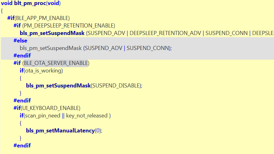
There are 2 scenarios that will make MCU enter deepsleep.
-
First one is if there’s no event for 60s, MCU will enter deepsleep. The events here include keys being pressed, so there is no drive pin high at this point to make deepsleep inaccessible.
-
The other scenario is if a key is stuck for more than 60s, MCU will enter deepsleep. Under the second scenario, the SDK will invert polarity from high level trigger to low level trigger to solve the problem.
BLE System Low Power Management
Based upon understanding of PM principle of this BLE SDK, user can configure PM under different application scenarios, referring to the demo “8208_ble_sample” low power management code as explained below.
Function blt_pm_proc is added in PM configuration of main_loop. This function must be placed at the end of main_loop to ensure it is immediate to blc_sdk_main_loop in time, since blt_pm_proc needs to configure low power management according to different UI entry tasks.
Summary of highlights in blt_pm_proc function:
(1) When some tasks need to turn off sleep mode, set bltm.suspend_mask to SUSPEND_DISABLE.
(2) After advertising for 60s in Advertising state, MCU enters deepsleep with wakeup source set to GPIO PAD in user initialization. The 60s timeout is determined by software timer using advertise_begin_tick variable to capture advertising start time.
The design of 60s into deepsleep is to save power, prevent slave wasting power on advertising even when not connected with master. User can justify 60s setting based on different applications.
(3) At Conn state slave role, under conditions of no key press, no audio or LED task for over 60s from last task, MCU enters deepsleep with GPIO PAD as wakeup source, and at the same time set DEEP_ANA_REG0 label in deepsleep register, so that once after wakeup slave will connect quickly with master.
The design of 60s into deepsleep is to save power. Actually if power consumption under connected state is tuned low enough as with deepsleep retention, it is not absolutely necessary to enter deepsleep.
To enter deepsleep at Conn state slave role, slave first issues a TERMINATE command to master by calling bls_ll_terminateConnection, after receiving ack which triggers BLT_EV_FLAG_TERMINATEcallback function, slave will enter deepsleep. If slave enters deepsleep without sending any request, since master is still at connected state and would constantly try to synchoroniz with slave till connection timeout. The connection timeout could be a very large value, e.g. 20s. If slave wakes up before 20s, slave would send advertising packet attempting to connect with master. But since master would assume it is already in connected state, it would not be able to connect to slave, and user experience is therefore very slow reconnection.
(4) If certain task can not be disrupt by long sleep time, user_latency can be set to 0, so latency_use is 0.
Under applications such as key_not_released, or DEVICE_LED_BUSY, call API bls_pm_setManualLatency to set user_latency to 0. When conn_interval is 10ms, sleep time is no more than 10ms.
(5) For scenario as in item 4, with latency set to 0, slave will wakeup at every conn interval, power might be unnecessarily too high since key scan and LED task does not repeat on every conn interval. Further power optimization can be done as following:
When LONG_PRESS_KEY_POWER_OPTIMIZE=1, once key press is stable (key_matrix_same_as_last_cnt > 5), manually set latency. With bls_pm_setManualLatency (3), sleep time will not exceed 4 *conn_interval. If conn_interval=10 ms, MCU will wake up every 40ms to process LED task and keyscan.
User can tweak this approach toward different conn intervals and task response time requirements.
Timer Wake-up by Application Layer
At Advertising state or Conn state Slave role, without GPIO PAD wakeup, once MCU enters sleep mode, it only wakes up at T_wakeup pre-determined by BLE SDK. User can not wake up MCU at an earlier time which might be needed at certain scenario. To provide more flexibility, application layer wakeup and associated callback function are added in the SDK:
Application layer timer wakeup API:
void bls_pm_setAppWakeupLowPower(u32 wakeup_tick, u8 enable);
“wakeup_tick” is wakeup time at System Timer tick value.
“enable”: 1-wakeup is enabled; 0-wakeup is disabled.
Registered call back function bls_pm_registerAppWakeupLowPowerCb is executed at application layer wakeup:
typedef     void (*pm_appWakeupLowPower_callback_t)(int);
void        bls_pm_registerAppWakeupLowPowerCb(pm_appWakeupLowPower_callback_t cb);
Take Conn state Slave role as an example:
When the user uses bls_pm_setAppWakeupLowPower to set the app_wakeup_tick for the application layer to wake up regularly, the SDK will check whether app_wakeup_tick is before T_wakeup before entering sleep.
-
If app_wakeup_tick is before T_wakeup, as shown in the figure below, it will trigger sleep in app_wakeup_tick to wake up early;
-
If app_wakeup_tick is after T_wakeup, MCU will still wake up at T_wakeup.
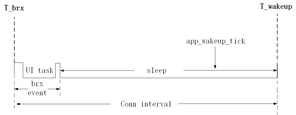
Low Battery Detect
Battery power detect/check, which may also appear in the Telink BLE SDK and related documentation under other names, includes: battery power detect/check, low battery detect/check low power detect/check), battery detect/check, etc. For example, the relevant files and functions in the SDK are named battery_check, battery_detect, battery_power_check, etc.
This document is unified under the name of "low battery detect".
The Importance of Low Battery Detect
For battery-powered products, as the battery power will gradually drop, when the voltage is low to a certain value, it will cause many problems.
a) The operating voltage range of 8208 chip is 1.8V~3.6V. When the voltage is lower than 1.8V, 8208 chip can no longer guarantee stable operation.
b) When the battery voltage is low, due to the unstable power supply, the "write" and "erase" operations of Flash may have the risk of error, causing the program firmware and user data to be modified abnormally, and eventually causing the product to fail. Based on our previous mass production experience, we set the low voltage threshold for this risk to 2.0V.
According to the above description, for battery-powered products, a secure voltage must be set, and the MCU is allowed to continue working only when the voltage is higher than this secure voltage; once the voltage falls below the secure voltage, the MCU stops running and needs to be shutdown immediately (this is achieved by entering deepsleep mode on the SDK).
The secure voltage is also called alarm voltage, and the value of this voltage is 2.0 V by default in the SDK.
Note:
The low voltage protection threshold 2.0V is an example and reference value. Customers should evaluate and modify these thresholds according to the actual situation. If users have unreasonable designs in the hardware circuit, which leads to a decrease in the stability of the power supply network, the safety thresholds must be increased as appropriate.
For the product developed and implemented using Telink BLE SDK, as long as the use of battery power, low power detection must be a real-time operation of the task for the product's entire life cycle to ensure the stability of the product.
The protection of low voltage detection for flash operation will be introduced further in the chapter on flash.
The Implementation of Low Battery Detect
The low battery detect requires the use of ADC to measure the power supply voltage. Users can refer to the 8208 Datasheet and Driver SDK Developer Handbook chapter on ADC to get the necessary understanding of the B80 ADC module first.
The implementation of the low battery detect is described in the SDK demo "8208_ble_sample", refer to the files vendor/common/battery_check.h and vendor/common/battery_check.c.
Make sure the macro "BATT_CHECK_ENABLE" is enabled in app_config.h. This macro is disabled by default, and users need to pay attention to it when using the low battery detect function.
#define BATT_CHECK_ENABLE 1
Notes on Low Battery Detect
Low battery detect is a basic ADC sampling task, and there are a number of issues that need attention when implementing an ADC to sample the supply voltage, as described below.
(1) VBAT Input Channel Recommended
The 8208 ADC input channels support ADC sampling of the supply voltage on the "VCC/VBAT" input channel, which corresponds to the last "VBAT" in the variable ADC_InputPchTypeDef below.
The available GPIO input channels are the input channels corresponding to PB0~PB7, PC4, and PA3.
/*ADC analog positive input channel selection enum*/
typedef enum {
……
    B0P,
    B1P,
    B2P,
    B3P,
    B4P,
    B5P,
    B6P,
    B7P,
    C4P,
    A3P,
……
    VBAT,
}ADC_InputPchTypeDef;
Currently "8208_ble_sample" selects VBAT input channel sampling.
(2) Differential Mode Only
Although the 8208 ADC input mode supports both Single Ended Mode and Differential Mode, for some specific reasons, Telink specifies that only Differential Mode can be used, and Single Ended Mode is not allowed.
The differential mode input channel is divided into positive input channel and negative input channel, the measured voltage is the voltage difference obtained by subtracting the negative input channel voltage from the positive input channel voltage.
If the ADC sample has only one input channel, when using differential mode, set the current input channel as the positive input channel and GND as the negative input channel, so that the voltage difference between the two is equal to the positive input channel voltage.
The differential mode is used in SDK low battery detect. The adc_set_input_mode_chn_misc function is called in the adc_init() function to select the differential mode. The code is as follows.
void adc_init(void){
...
    adc_set_input_mode_chn_misc(DIFFERENTIAL_MODE);
...
}
(3) Must Use Dfifo Mode To Obtain ADC Sampling Value
For 8208, Telink stipulates that only Dfifo mode can be used to read ADC sampling values. Refer to the following function.
unsigned int adc_sample_and_get_result(void);
(4) Need To Switch Different ADC Tasks
Refer to the "8208 Datasheet" that the ADC state machine has only Misc channel.
(5) Low Battery Detect Initialization
Refer to the initialization implementation of the app_battery_power_check function.
The order of ADC initialization must satisfy the following procedure: first power off sar adc, then configure other parameters, and finally power on sar adc. All initialization of ADC sampling must follow this flow.
adc_init();
adc_vbat_channel_init();
adc_power_on_sar_adc(1);
For the configuration before sar adc power on and power off, the user try not to modify, and use the default settings.
The adc_vbat_detect_init initialization function is called in app_battery_power_check with the following code:
if(!adc_hw_initialized){
        adc_hw_initialized = 1;
        adc_init();
        adc_vbat_channel_init();
        adc_power_on_sar_adc(1);
    }
Here a variable adc_hw_initialized is used, which is called once only when it is 0 and set to 1; it is not initialized again when it is 1. The adc_hw_initialized is also manipulated in the following API.
void battery_set_detect_enable (int en)
{
    lowBattDet_enable = en;
    if(!en){
        adc_hw_initialized = 0;   //need initialized again
    }
}
The functions that can be implemented by a design using adc_hw_initialized are:
a. Switching with other ADC task
The effect of sleep mode (suspend/deepsleep retention) is not considered first, and only the switching between low battery detect and other ADC tasks is analyzed.
Because of the need to consider the switch between low battery detect and other ADC tasks, adc init may be executed several times, so it cannot be written to user initialization and must be implemented in main_loop.
The first time the app_battery_power_check function is executed, adc init is executed and will not be executed repeatedly.
Once the "ADC other task" needs to be executed, it will take away the ADC usage and make sure that the "ADC other task" must call battery_set_detect_enable(0) when it is initialized, which will clear adc_hw_initialized to 0.
When the "ADC other task" is finished, the right to use the ADC is handed over. The app_battery_power_check is executed again, and since the value of adc_hw_initialized is 0, adc_vbat_detect_init must be executed again. This ensures that the low battery detect is reinitialized each time it is switched back.
b. Adaptive handling of suspend and deepsleep retention
Take sleep mode into account.
The adc_hw_initialized variable must be defined as a variable on the "data_reload" segment, not on the "data" or "bss". Defining it on the "data_reload" segment ensures that this variable is used after each deepsleep retention wake_up when the software bootloader is executed (i.e., cstartup_xxx. S) will be re-initialized to 0; after sleep wake_up, this variable can be left unchanged.
The common feature of the register configured inside the adc_vbat_detect_init function is that it does not power down in suspend mode and can maintain the state; it will power down in deepsleep retention mode.
If the MCU enters into suspend mode, when it wakes up and executes app_battery_power_check again, the value of adc_hw_initialized is the same as before suspend, so there is no need to re-execute the adc_vbat_detect_init function.
If the MCU enters deepsleep retention mode and wakes up with adc_hw_initialized to 0, adc_vbat_detect_init must be re-executed and the ADC-related register state needs to be reconfigured.
The state of register set in the adc init function can be kept from powering down during the suspend.
Refer to the "Low Power Management" section that the Dfifo related registers will be powered down in suspend mode, so the following two codes are not put in the adc init function, but in the app_ battery_power_check function, to ensure that it is reset before each low power detection.
  adc_config_misc_channel_buf((u16 *)adc_dat_buf,ADC_SAMPLE_NUM<<2);
  dfifo_enable_dfifo2();
(6) Low Battery Detect Processing
In main_loop, the app_battery_power_check function is called to implement the processing of low battery detect, and the related code is as follows.
u8      lowBattDet_enable = 1;
_attribute_data_reload_ u8      adc_hw_initialized = 0;   //note: can not be retention variable
void battery_set_detect_enable (int en)
{
    lowBattDet_enable = en;

    if(!en){
        adc_hw_initialized = 0;   //need initialized again
    }
}
int battery_get_detect_enable (void)
{
    return lowBattDet_enable;
}
if(battery_get_detect_enable() && clock_time_exceed(lowBattDet_tick, 500000) ){
    lowBattDet_tick = clock_time();
    app_battery_power_check(VBAT_ALRAM_THRES_MV);
}
The default value of lowBattDet_enable is 1. Low battery detect is allowed by default, and the MCU can start low battery detect immediately after powering up. This variable needs to be set to retention_data to ensure that deepsleep retention cannot modify its state.
The value of lowBattDet_enable can only be changed when other ADC tasks need to seize ADC usage: when other ADC tasks start, battery_set_detect_enable(0) is called, at this time app_battery_power_check is not called again in main_loop; After the other ADC tasks are finished, call battery_set_detect_enable(1) to surrender the right to use ADC, then the app_battery_power_check function can be called again in main_loop.
The frequency of low battery detect is controlled by the variable lowBattDet_tick, which is executed every 500ms in the demo. Users can modify this time according to their needs.
The specific implementation of the app_battery_power_check function seems to be cumbersome, involving the initialization of low-power detection, Dfifo preparation, data acquisition, data processing, low-power alarm processing, etc.
The ADC sampling data is acquired using Dfifo mode. Dfifo samples 8 strokes of data by default and calculates the average value after removing the maximum and minimum values.
The adc_init function shows that the period of each adc sample is 10.4us, so the data acquisition process is about 83us.
The macro "ADC_SAMPLE_NUM" in the demo can be modified to 4, which shortens the ADC sampling time to 41 us. it is recommended to use the method of 8 data strokes for more accurate calculation results.
#define ADC_SAMPLE_NUM       8

#if (ADC_SAMPLE_NUM == 4)   //use middle 2 data (index: 1,2)
    u32 adc_average = (adc_sample[1] + adc_sample[2])/2; #elif(ADC_SAMPLE_NUM == 8)     //use middle 4 data (index: 2,3,4,5)
    u32 adc_average = (adc_sample[2] + adc_sample[3] + adc_sample[4] +
adc_sample[5])/4;
#endif
(7) Low Voltage Alarm
The parameter alram_vol_mv of app_battery_power_check is to specify the alarm voltage in mV for low battery detect. According to the previous content, the default setting in SDK is 2000 mV. In the low voltage detection of main_loop, when the power supply voltage is lower than 2000 mV, it enters low voltage range.
The demo code for handling low voltage alarm is shown below. The MCU must be shutdown after low voltage, and no other work can be done.
The "8208_ble_remote" uses the way of entering deepsleep to shut down the MCU, and a button is set to wake.
In addition to shutdown, user can modify other alarm behaviors for low voltage alarm processing.
In the code below, 3 quick flashes are made using LED lights to inform the product user that the battery needs to be charged or replaced.
u8 battery_check_returnVaule = 0;
if(analog_read(USED_DEEP_ANA_REG) & LOW_BATT_FLG){
    battery_check_returnVaule = app_battery_power_check(VBAT_ALRAM_THRES_MV + 200);  //2.2 V
}
else{
    battery_check_returnVaule = app_battery_power_check(VBAT_ALRAM_THRES_MV);  //2.0 V
}
if(battery_check_returnVaule){
    analog_write(USED_DEEP_ANA_REG,  analog_read(USED_DEEP_ANA_REG)&(~LOW_BATT_FLG));  //clr
}
else{
    #if (UI_LED_ENABLE)  //led indicate
        for(int k=0;k<3;k++){
            gpio_write(GPIO_LED_BLUE, LED_ON_LEVAL);
            sleep_us(200000);
            gpio_write(GPIO_LED_BLUE, !LED_ON_LEVAL);
            sleep_us(200000);
        }
    #endif
    analog_write(USED_DEEP_ANA_REG,  analog_read(USED_DEEP_ANA_REG) | LOW_BATT_FLG);  //mark
    GPIO_WAKEUP_FEATURE_LOW;

    cpu_set_gpio_wakeup (GPIO_WAKEUP_FEATURE, Level_High, 1);  //drive pin pad high wakeup deepsleep

    cpu_sleep_wakeup(DEEPSLEEP_MODE, PM_WAKEUP_PAD, 0);  //deepsleep
}
After "8208_ble_remote" is shutdown, they enter the deepsleep mode where they can be woken up. If a key wake-up occurs, the SDK will do a quick low battery detect during user initialization instead of waiting until the main_loop. The reason for this process is to avoid application errors, as illustrated by the following example.
If the product user has been alerted by the flashing LED during the low power alarm and then wakes up again by entering deepsleep, it takes at least 500ms to do the low battery detect from the processing of main_loop. Before 500ms, the slave's broadcast packet has been sent for a long time, and it is likely to be connected to the master already. In this case, there is a bug that the device already having low power alarm continues to work again.
For this reason, the SDK must do the low battery detect in advance during user initialization, and must prevent the above situation from happening at this step. So add low battery detect during user initialization, and the function interface in the SDK is:
if(analog_read(USED_DEEP_ANA_REG) & LOW_BATT_FLG){
            battery_check_returnVaule = app_battery_power_check(VBAT_ALRAM_THRES_MV + 200);  //2.2 V
        }
        else{
            battery_check_returnVaule = app_battery_power_check(VBAT_ALRAM_THRES_MV);  //2.0 V
        }
According to the value of USED_DEEP_ANA_REG analog register can determine whether the low power alarm shutdown is woken up, at this time, a fast low power detection is performed and the previous 2000mV alarm voltage is increased to 2200mV (called recovery voltage). The reason for the 200mV increase is:
Low voltage detection will have some errors, can not guarantee the accuracy and consistency of the measurement results. For example, if the error is 20mV, the voltage detected for the first time may be 1990mV to enter shutdown mode, and then the voltage value detected again after waking up in user initialization is 2005mV. If the alarm voltage is still 2000mV, it still can't stop the bug described above.
Therefore, it is necessary to adjust the alarm voltage slightly higher than the maximum error of low power detection during the fast low power detection after the shutdown mode wakeup.
Only when a certain low power detection found that the voltage is lower than 2000mV into shutdown mode, the recovery voltage 2200mV will appear, so user does not have to worry about this 2200mV will misreport low voltage to the actual voltage 2V~2.2V products. Product users see the low voltage alarm indication, after charging or replacing the battery to meet the requirements of recovery voltage, the product back to normal use.
OTA
In order to realize the OTA function of the 8208 BLE slave, a device is required as a BLE OTA master.
The OTA master can be a Bluetooth device actually used with the slave (you need to implement OTA in the APP), or you can use Telink's BLE master kma dongle. The following uses Telink's BLE master kma dongle as the ota master to introduce OTA in detail. The related code implementation can also be found in feature_ota_big_pdu under the Multi-Connection SDK.
8208 supports Flash multi-address boot: In addition to the first address of Flash 0x00000, 128K Flash also supports reading firmware from Flash high addresses 0x10000 (64K), 512K Flash also supports reading firmware from Flash high addresses 0x10000 (64K), 0x20000 (128K) and 0x40000 (256K). This document uses high address 0x20000 as an example to introduce OTA.
Flash Architecture and OTA Procedure
Flash Storage Architecture
When booting address is 0x20000, size of firmware compiled by the SDK should not exceed 128kB, i.e. the flash area 0~0x20000 serves to store firmware. If your firmware size is larger than 128K, then you would need to use 0x0 and 0x40000 as boot address to alternate OTA upgrade, the firmware size shouldn’t be larger than 240K. This is because 0x7C000 ~ 0x7FFFF need to store some SDK related information. For details, please refer to the introduction in the Flash chapter. In addition, for 128K Flash, use the boot address as 0 and 0x10000 to alternate OTA upgrade, the firmware size shouldn’t be larger than 48K.

(1) OTA Master burns new firmware2 into the Master flash area from 0x20000 to 0x40000.
(2) OTA for the first time:
-
When power on, Slave starts booting and executing firmware1 from flash 0~0x20000.
-
When firmware1 is running, the area of Slave flash starting from 0x20000 (i.e. flash 0x20000~0x40000) is cleared during initialization and will be used as storage area for new firmware.
-
OTA process starts, Master transfers firmware2 into Slave flash area from 0x20000 to 0x40000 via RF. Then slave reboot (Restart, similar to a power outage and power on again).
(3) For subsequent OTA updates, OTA Master first burns new firmware3 into the Master flash area from 0x20000 to 0x40000.
(4) OTA for the second time:
-
When power on, Slave starts booting and executing firmware2 from flash 0x20000~0x40000.
-
When firmware2 is running, the area of Slave flash starting from 0x0 (i.e. flash 0~0x20000) is cleared during initialization and will be used as storage area for new firmware.
-
OTA process starts, Master transfers firmware3 into Slave flash area 0~0x20000 via RF. Then slave reboot (Restart, similar to a power outage and power on again).
(5) Subsequent OTA process repeats steps (1) ~ (4), which can be understood as (2) represents OTA of the (2n+1)-th time, while (4) represents OTA of the (2n+2)-th time.
OTA Update Procedure
Based on the flash storage structure introduced, the OTA update procedure is illustrated as below:
First introduce the multi-address booting mechanism (only the first two booting addresses 0x00000 and 0x20000 will be introduced here): after MCU is powered on, it boots from address 0 by default. First, read the content of flash 0x08. If the value is 0x4b, the code starting from 0 are transferred to RAM, and the following instruction fetch address equals 0 plus PC pointer value; if the value of 0x08 is not 0x4b, the MCU directly reads the value of 0x20008, if the value is 0x4b, the MCU moves the code from 0x20000 to RAM, and all subsequent fetches start from the 0x20000 address, that is, the fetch address = 0x20000+PC pointer value.
So as long as you modify the value of the 0x08 and 0x20008 flag bits, you can specify which part of the FLASH code that the MCU executes.
The power-on and OTA process of a certain SDK (2n+1 or 2n+2) is:
(1) The MCU is powered on, and the values of 0x08 and 0x20008 are read and compared with 0x4b to determine the booting address, and then boots from the corresponding address and execute the code. This function is automatically completed by the MCU hardware.
(2) During the program initialization process, read the MCU hardware register to determine which address the MCU boots from:
If boots from 0, set ota_program_offset to 0x20000, and erase all non-0xff content in the 0x20000 area to 0xff, which means that the new firmware obtained by the next OTA will be stored in the area starting at 0x20000;
If boots from 0x20000, set ota_program_offset to 0x0, and erase all the non-0xff content in the 0x0 area to 0xff, which means that the new firmware obtained by the next OTA will be stored in the area starting from 0x0.
(3) Slave MCU executes the firmware after booting; OTA Master is powered on and establishes BLE connection with Slave.
(4) Trigger OTA Master to enter OTA mode by UI (e.g. button press, write memory by PC tool, etc.). After entering OTA mode, OTA Master needs to obtain Handle value of Slave OTA Service Data Attribute (The handle value can be pre-appointed by Slave and Master, or obtained via "read_by_type".)
(5) After the Attribute Handle value is obtained, OTA Master may need to obtain version number of current Slave Flash firmware, and compare it with the version number of local stored new firmware.
Note:
Users need to obtain the version number by themselves.
(6) To enable OTA upgrade, OTA Master will send an OTA_start command to inform Slave to enter OTA mode.
(7) After the OTA_start command is received, Slave enters OTA mode and waits for OTA data to be sent from Master.
(8) Master reads the firmware stored in the flash area starting from 0x20000, and continuously sends OTA data to Slave until the entire firmware is sent.
(9) Slave receives OTA data and stores it in the area starting with ota_program_offset.
(10) After the master sends all the OTA data, check whether the data is received correctly by the slave (call the relevant function of the underlying BLE to determine whether the data of the link layer is correctly acknowledged).
(11) After the master confirms that all OTA data has been correctly received by the slave, it sends an OTA_END command.
(12) Slave receives the OTA_END command and writes the offset address of the new firmware area 0x08 (that is, ota_program_offset+0x08) as 0x4b, and writes the offset address of the old firmware storage area 0x08 as 0x00, which means it will Move code execution from the new area.
(13) Reboot the slave, the new firmware takes effect.
During the whole OTA upgrade process, Slave will continuously check whether there’s packet error, packet loss or timeout (A timer is started when OTA starts). Once packet error, packet loss or timeout is detected, Slave will determine the OTA process fails. Then Slave reboots, and executes the old firmware.
The OTA related operations on Slave side described above have been realized in the SDK and can be used by user directly. On Master side, extra firmware design is needed and it will be introduced later.
Modify FW Size and Booting Address
API blc_ota_setFirmwareSizeAndBootAddress supports modifying the boot address and the maximum firmware size. Herein booting address means the address except 0 to store New_firmware, so it should be one of 0x10000, 0x20000 or 0x40000.
| Flash size | Firmware_Boot_address | Firmware size (max)/K |
|---|---|---|
| 128 | 0x10000 | 48 |
| 512 | 0x10000 | 64 |
| 512 | 0x20000 | 128 |
| 512 | 0x40000 | 240 |
The default maximum firmware size in the SDK is 240K, and the corresponding startup addresses are 0x00000 and 0x40000. User can call API blc_ota_setFirmwareSizeAndBootAddress to set the maximum firmware size.
ble_sts_t blc_ota_setFirmwareSizeAndBootAddress(int firmware_size_k, multi_boot_addr_e new_fw_addr);
The setting of firmware_size_k must be 4K byte aligned. For example, when the size is 97K, it needs to be set to 100K.
The parameter multi_boot_addr_e indicates the available boot addresses, including three.
typedef enum{
    MULTI_BOOT_ADDR_0x10000     = 0x10000,  //64 K
    MULTI_BOOT_ADDR_0x20000     = 0x20000,  //128 K
    MULTI_BOOT_ADDR_0x40000     = 0x40000,  //256 K
}multi_boot_addr_e;
This API can only be called before cpu_wakeup_init in main function, otherwise it is invalid. The reason is that the cpu_wakeup_init function needs to do some settings according to the values of firmware_size and boot_addr.
If the firmware does not need such a large space, for example, the firmware size does not exceed 60kB, use only part of the two 128kB spaces (0x00000 ~ 0x20000, 0x20000 ~ 0x40000). To use the redundant space as data storage area, you can perform the following settings.
blc_ota_setFirmwareSizeAndBootAddress(60, 0x20000);
With the above configuration, two 60kB Flash areas 0x00000 ~ 0x0F000 and 0x20000 ~ 0x2F000 can be used as storage space for firmware, while two 68kB Flash areas 0x0F000 ~ 0x20000 and 0x2F000 ~ 0x40000 can be used as storage space for user data.
The 128kB Flash OTA is basically the same as the 512kB, except that the offset needs to be configured to 0x10000.
(1) For 128kB Flash, the default maximum firmware size supported by the SDK is 48kB.
(2) For 128kB Flash, by modifying the SDK configuration as shown below, the firmware can be up to 56kB in size, but there will be no additional Flash space to store user data.
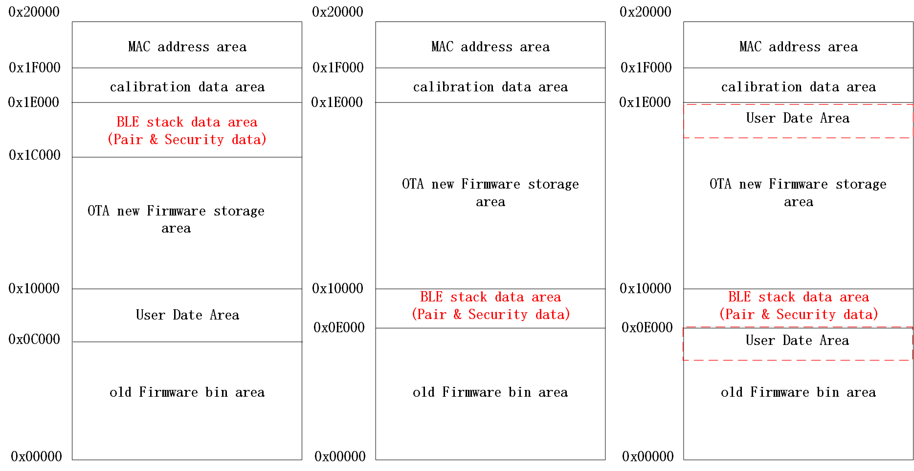
RF Data Processing for OTA Mode
OTA Processing in Attribute Table
OTA related contents needs to be added in the Attribute Table on slave end. The "att_readwrite_callback_t r" and "att_readwrite_callback_t w" of the OTA data Attribute should be set as otaRead and otaWrite, respectively; the attribute should be set as Read and Write_without_Rsp (Telink Master KMA Dongle sends data via "Write Command" by default, with no need of ack from Slave to enable faster speed).
// OTA attribute values
static const u8 my_OtaCharVal[19] = {
    CHAR_PROP_READ | CHAR_PROP_WRITE_WITHOUT_RSP,
    U16_LO(OTA_CMD_OUT_DP_H), U16_HI(OTA_CMD_OUT_DP_H),
    TELINK_SPP_DATA_OTA,
};

    {4,ATT_PERMISSIONS_READ, 2,16,(u8*)(&my_primaryServiceUUID),    (u8*)(&my_OtaServiceUUID), 0},
    {0,ATT_PERMISSIONS_READ, 2, sizeof(my_OtaCharVal),(u8*)(&my_characterUUID), (u8*)(my_OtaCharVal), 0},
    {0,ATT_PERMISSIONS_RDWR,16,sizeof(my_OtaData),(u8*)(&my_OtaUUID),   (&my_OtaData), &otaWrite, NULL},
    {0,ATT_PERMISSIONS_READ, 2,sizeof (my_OtaName),(u8*)(&userdesc_UUID), (u8*)(my_OtaName), 0},
When Master sends OTA data to Slave, it actually writes data to the second Attribute as shown above, so Master needs to know the Attribute Handle of this Attribute in the Attribute Table. To use the Attribute Handle value pre-appointed by Master and Slave, user can directly define it on Master side.
OTA Protocol
The master sends commands and data to the slave through the Write Command of the L2CAP layer.
OTA_CMD composition:
The PDUs of OTA's CMD are as follows.
| OTA Command Payload | - |
|---|---|
| Opcode (2 octet) | invalid data |
Opcode:
| Opcode | Name |
|---|---|
| 0xFF00 | CMD_OTA_VERSION |
| 0xFF01 | CMD_OTA_START |
| 0xFF02 | CMD_OTA_END |
(1) CMD_OTA_VERSION
It is a command to get the current firmware version number of the slave, and the user can choose to use it. This command can be used to pass the firmware version number through the callback function reserved on the slave end.
void blc_ota_registerOtaFirmwareVersionReqCb(ota_versionCb_t cb);
The server side will trigger this callback function when it receives the CMD_OTA_VERSION command.
(2) CMD_OTA_START
This command is the OTA update start command. The master sends this command to the slave to officially start the OTA update.
(3) CMD_OTA_END
This command is the end command. When Master confirms all OTA data are correctly received by Slave, it will send this command, which can be followed by four valid bytes to re-confirm Slave has received all data from Master.
| - | CMD_data | - |
|---|---|---|
| Adr_index_max (2 octets) | Adr_index_max_xor (2 octets) | Reserved |
-
Adr_index_max: the maximum adr_index value
-
Adr_index_max_xor: the anomaly value of Adr_index_max for verification
-
Reserved: Reserved for future function extension
OTA_Data introduction:
| - | OTA PDU | - |
|---|---|---|
| Adr_Index (2 octets) | Data(16 octets) | CRC (2 octets) |
Note:
OTA PDU length fixed size is 16 octets
OTA_PDU Format:
When the range of the first two bytes is within firmware_size_k, it represents an OTA data. Since the firmware size does not exceed 128K (0x20000), the OTA data packet transmits 16 byte of firmware data each time, and the adr_index used is the value of the actual firmware address divided by 16. adr_index=0 means the OTA data is the value of firmware address The adr_index=0 means the OTA data is the value of firmware address 0x0 ~ 0xF; adr_index=1 means the OTA data is the value of firmware address 0x10 ~ 0x1F. The last two bytes are a CRC_16 calculation of the previous Adr_Index and Data to get the first CRC value, the slave will do the same CRC calculation after receiving the OTA data, and only when the CRC calculated by both matches, it will be considered a valid data.
RF Transfer Processing Method
Based on the premise of BLE link layer RF data auto-ack to ensure that all packets are not lost, OTA data transform does not check whether each OTA data is ack, i.e., after the master sends an OTA data by write command, it does not check whether the other party has ack information reply in software, as long as the master hardware TX buffer cache of data to be sent does not reach a certain number, the next data is directly dropped into TX buffer.
The following will introduce the specific implementation process of OTA and elaborate the interaction process between Salve and Master in the whole RF Transform.
OTA implementation:
The OTA-related operations on the master side are:
(1) Check if there’s any behavior to trigger entering OTA mode. If so, Master enters OTA mode.
(2) To send OTA commands and data to Slave, Master needs to know the Attribute Handle value of current OTA data Atrribute on Slave side. User can decide to directly use the pre-appointed value or obtain the Handle value via "Read By Type Request".
UUID of OTA data in Telink BLE SDK is always 16-byte value as shown below:
#define TELINK_SPP_DATA_OTA {0x12,0x2B,0x0d,0x0c,0x0b,0x0a,0x09,0x08,0x07,0x06,0x05,0x04,0x03,0x02,0x01,0x00}
In "Read By Type Request" from Master, the "Type" is set as the 16-byte UUID. The Attribute Handle for the OTA UUID is available from "Read By Type Rsp" responded by Slave. In the figure below, the Attribute Handle value is shown as "0x0031".

(3) Obtain the current firmware version number of the slave and decide whether to continue the OTA update (if the version is already the latest, no update is required). This step is for the user to choose whether to do it or not. The BLE SDK does not provide a specific version number acquisition method, users can play by themselves. In the current B80 BLE SDK, it does not implement version number transmission. The user can use write cmd to send a request to obtain the OTA version to the slave through the OTA version cmd, but the slave side only provides a callback function when receiving the OTA version request, and the user finds a way to set the slave side in the callback function. The version number is sent to the master (such as manually sending a NOTIFY/INDICATE data).
(4) Start a timing at the beginning of the OTA, and then continue to check whether the timing exceeds 30 seconds (this is only a reference time, and the actual evaluation will be made after the normal OTA required by the user test).
If it takes more than 30 seconds to consider the OTA timeout failure, because the slave side will check the CRC after receiving the OTA data. Once the CRC error or other errors (such as programming flash errors) occur, the OTA will be considered as a failure and the program will be restarted directly. The layer cannot ack the master, and the data on the master side has not been sent out, resulting in a timeout.
(5) Read the four bytes of Master flash 0x20018~0x2001b to determine the size of the firmware.
This size is implemented by our compiler. Assuming the size of the firmware is 20k = 0x5000, then the value of 0x18~0x1b of the firmware is 0x00005000, so the size of the firmware can be read from 0x20018~0x2001b.
In the bin file shown in the figure below, the content of 0x18 ~ 0x1b is 0x0000A164, so the size is 0xa164 = 41316Bytes, from 0x0000 to 0xa164.
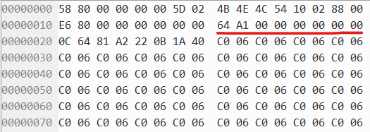
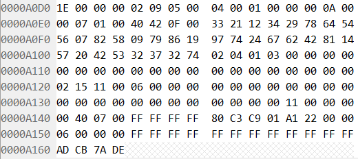
(6) Master sends an OTA start command "0xff01" to Slave, so as to inform it to enter OTA mode and wait for OTA data from Master, as shown below.

(7) Read 16 bytes of firmware each time starting from Master flash 0x20000, assemble them into OTA data packet, set corresponding adr_index, calculate CRC value, and push the packet into TX FIFO, until all data of the firmware are sent to Slave.
The data sending method is described above, using the OTA data format: 20-byte valid data contains 2-byte adr_index, 16-byte firmware data and 2-byte CRC value to the former 18 bytes.
Note: If firmware data for the final transfer are less than 16 bytes, the remaining bytes should be complemented with "0xff" and need to be considered for CRC calculation.
Below illustrates how to assemble OTA data.
Data for first transfer: "adr_index" is "0x00 00", 16-byte data are values of addresses 0x0000 ~ 0x000f. Suppose CRC calculation result for the former 18 bytes is "0xXYZW", the 20-byte data should be:
0x00 0x00 0x58 0x80 .... (12 bytes not listed)..... 0x88 0x00 0xZW 0xXY
Data for second transfer:
0x01 0x00 0xE6 0x80 ....(12 bytes not listed)..... 0x00 0x00 0xJK 0xHI
Data for third transfer:
0x02 0x00 0x0C 0x64 ....(12 bytes not listed)..... 0xC0 0x06 0xNO 0xLM
........
Data for penultimate transfer:
0x15 0x0a 0x06 0x00 ....(12 bytes not listed)..... 0xff 0xff 0xST 0xPQ
Data for final transfer:
0x16 0x0a 0xad 0xcb 0x7a 0xde 0xff 0xff 0xff 0xff 0xff 0xff 0xff 0xff 0xff 0xff 0xff 0xff 0xWX 0xUV
12 "0xff" are added to complement 16 bytes.
The CRC calculation result for a total of 18 bytes from 0x16 to 0xff is 0xUVWX.
The above data is shown in the figure below:


(8) After the firmware data is sent, check whether the data of the BLE link layer has been completely sent (because only when the data of the link layer is acked by the slave, the data is considered to be sent successfully). If it is completely sent, the master sends an ota_end command to notify the slave that all data has been sent.
The packet effective bytes of the OTA end are set to 6, the first two are 0xff02, and the middle two bytes are the maximum adr_index value of the new firmware (this is for the slave to confirm again that the last or several OTA data is not lost) , The last two bytes are the inverse of the largest adr_index value in the middle, which is equivalent to a simple check. OTA end does not require CRC check.
Take the bin shown in the above figure as an example, the largest adr_index is 0x0a16, and its inverse value is 0xf5e9, and the final OTA end package is shown in the figure above.
(9) Check if link-layer TX FIFO on Master side is empty: If it’s empty, it indicates all data and commands in above steps are sent successfully, i.e. OTA task on Master succeeds.
Please refer to Appendix for CRC_16 calculation function.
As introduced above, Slave can directly invoke the otaWrite and otaRead in OTA Attribute. After Slave receives write command from Master, it will be parsed and processed automatically in BLE stack by invoking the otaWrite function.
In the otaWrite function, the 20-byte packet data will be parsed: first judge whether it’s OTA CMD or OTA data, then process correspondingly (respond to OTA cmd; check CRC to OTA data and burn data into specific addresses of flash).
The OTA related operations on Slave side are shown as below:
(1) OTA_FIRMWARE_VERSION command is received: Master requests to obtain Slave firmware version number.
In this BLE SDK, after Slave receives this command, it will only check whether related callback function is registered and determine whether to trigger the callback function correspondingly.
The interface in ble_ll_ota.h to register this callback function is shown as below:
typedef void (*ota_versionCb_t)(void);
void blc_ota_registerOtaFirmwareVersionReqCb(ota_versionCb_t cb);
(2) OTA start command is received: Slave enters OTA mode.
If the "bls_ota_registerStartCmdCb" function is used to register the callback function of OTA start, then the callback function is executed to modify some parameter states after entering OTA mode (e.g. disable PM to stabilize OTA data transfer).
And the slave also starts and maintains a slave_adr_index to record the adr_index of the latest correct OTA data. The slave_adr_index is used to check whether there’s packet loss in the whole OTA process, and its initial value is -1. Once packet loss is detected, OTA fails, Slave MCU exits OTA and reboots; since Master cannot receive any ack from Slave, it will discover OTA failure by software after timeout.
The following interface is used to register the callback function of OTA start:
typedef void (*ota_startCb_t)(void);
void blc_ota_registerOtaStartCmdCb(ota_startCb_t cb);
User needs to register this callback function to carry out operations when OTA starts, for example, configure LED blinking to indicate OTA process.
After Slave receives "OTA start", it enters OTA and starts a timer (The timeout duration is set as 30s by default in current SDK). If OTA process is not finished within 30s, it’s regarded as OTA failure due to timeout. User can evaluate firmware size (larger size takes more time) and BLE data bandwidth on Master (narrow bandwidth will influence OTA speed), and modify this timeout duration accordingly via the variable as shown below.
ble_sts_t blc_ota_setOtaProcessTimeout(int timeout_second);
The interface supports a timeout time range of 4 ~ 1000s, in s.
(3) Valid OTA data are received:
Whenever Slave receives one 20-byte OTA data packet, it will first check if the adr_index equals slave_adr_index plus 1. If not equal, it indicates packet loss and OTA failure; if equal, the slave_adr_index value is updated.
Then carry out CRC_16 check to the former 18 bytes. If not matched, OTA fails; if matched, the 16-byte valid data are written into corresponding flash area (ota_program_offset+adr_index16 ~ ota_program_offset+adr_index16 + 15). During flash writing process, if there’s any error, OTA also fails.
(4) "OTA end" command is received:
Check whether adr_max in OTA end packet and the inverted check value are correct. If yes, the adr_max can be used to double check whether maximum index value of data received by Slave from Master equals the adr_max in this packet. If equal, OTA succeeds; if not equal, OTA fails due to packet loss.
After successful OTA, Slave will set the booting flag of the old firmware address in flash as 0, set the booting flag of the new firmware address in flash as 0x4b, then reboot MCU.
(5) Slave supplies OTA state callback function:
After Slave starts OTA, MCU will finally reboot when OTA is successful.
If OTA succeeds, Slave will set flag before rebooting so that MCU executes the New_firmware.
If OTA fails, the incorrect new firmware will be erased before rebooting, so that MCU still executes the Old_firmware.
Before rebooting, user can judge whether the OTA state callback function is registered and determine whether to trigger it correspondingly.
The corresponding codes are as following:
enum{
    OTA_SUCCESS             = 0,            //success
    OTA_PACKET_LOSS,                        //lost one or more OTA PDU
    OTA_DATA_CRC_ERR,                       //packet PDU CRC err
    OTA_WRITE_FLASH_ERR,                    //write OTA data to flash ERR
    OTA_DATA_UNCOMPLETE,                    //lost last one or more OTA PDU
    OTA_TIMEOUT,                            //OTA flow total timeout
    OTA_FW_CHECK_ERR,                       //firmware CRC check error
    OTA_STEP_ERR,
};

typedef void (*ota_resIndicateCb_t)(int result);

void blc_ota_registerOtaResultIndicationCb (ota_resIndicateCb_t cb);
After the callback function is set, the 6 values of the parameter result of the callback function are as described in the enum above. The first is OTA success, and the rest are different reasons for failure.
Since the MCU reboot will be triggered after the callback function is executed, when the result of this status indication is seen in the actual code, there is not much functional use. The OTA upgrade success or failure will trigger the callback function, users can debug by the result of the function to return parameters. When the OTA is unsuccessful, you can read the above result and stop the MCU with while(1) to understand what causes the OTA failure.
OTA Security
OTA Service Data Security
OTA Service is a kind of GATT service, and the problem of OTA service security protection is the problem of BLE GATT service data security protection, that is, data cannot be accessed illegally. According to the design of BLE Spec, user can used the following methods:
(1) To enable SMP, it is recommended to use the Security Level as high as possible to achieve the function that only legally paired devices have access to OTA server data. Refer to the introduction of SMP in this document.
For example, using Security Mode 1 Level 3, the pairing of Authentication and MITM can effectively control the product slave device and the specific master to pair encryption success and back connection, the attacker cannot successfully encrypt with the slave device. Add the corresponding security level settings to the read and write of the protected GATT service data, and the attacker will not be able to access these data. If you use Mode 1 Level 4, Secure Connection + Authentication, the security level is even higher.
The codes that may be involved include the following:
typedef enum {
    LE_Security_Mode_1_Level_1 = BIT(0),  No_Authentication_No_Encryption           = BIT(0), No_Security = BIT(0),
    LE_Security_Mode_1_Level_2 = BIT(1),  Unauthenticated_Pairing_with_Encryption   = BIT(1),
    LE_Security_Mode_1_Level_3 = BIT(2),  Authenticated_Pairing_with_Encryption     = BIT(2),
    LE_Security_Mode_1_Level_4 = BIT(3),  Authenticated_LE_Secure_Connection_Pairing_with_Encryption = BIT(3),
}le_security_mode_level_t;

#define ATT_PERMISSIONS_AUTHOR               0x10 //Attribute access(Read & Write) requires Authorization
#define ATT_PERMISSIONS_ENCRYPT              0x20 //Attribute access(Read & Write) requires Encryption
#define ATT_PERMISSIONS_AUTHEN               0x40 //Attribute access(Read & Write) requires Authentication(MITM protection)
#define ATT_PERMISSIONS_SECURE_CONN          0x80 //Attribute access(Read & Write) requires Secure_Connection
#define ATT_PERMISSIONS_SECURITY             (ATT_PERMISSIONS_AUTHOR | ATT_PERMISSIONS_ENCRYPT | ATT_PERMISSIONS_AUTHEN | ATT_PERMISSIONS_SECURE_CONN)
(2) Use whitelist. Users can use the whitelist to connect only to the master device they want to connect to, or they can effectively intercept the attacker's connection.
(3) Use address privacy protection, local device and peer device use resolvable private address (RPA), which effectively hides the identity address of the other party or us and maks the connection more secure.
OTA RF Transmission Data Integrity
Since RF is an unstable transmission, a certain protection mechanism is needed to ensure the integrity and correctness of the firmware during the OTA process.
Refer to the previous introduction, the OTA master needs to divide the Firmware into multiple data packets according to a certain size in advance. The first 2 byte of each data packet is the packet sequence number, starting from 0 and increasing by 1.
(1) OTA PDU CRC16 Check
Refer to the previous introduction, on the basis of LinkLayer data protection, add a CRC16 checksum to the OTA protocol to make data transmission more secure.
(2) OTA PDU Serial Number Check
The OTA master splits the Firmware into several OTA PDUs, each PDU has its own package serial number.
For the convenience of explanation, assume the Firmware size is 50K, split according to OTA PDU 16Byte, the number of PDUs is 50*1024/16=3200, then the serial number is 0 ~ 3199, i.e. 0x0 ~ 0xC7F.
After the OTA starts, set the expected serial number to 0. For each OTA data received, use the expected serial number and the actual serial number to compare, only when the two are equal, the process is considered correct and the expected serial number is updated +1. If the two are not equal, the process is considered failed and the OTA is ended. This design can ensure the continuity and uniqueness of OTA PDUs.
At the end of OTA, you can read the serial number 0xC7F of the last OTA PDU of Firmware on the OTA_END packet, and use this serial number to compare with the actual maximum serial number received, you can determine whether the OTA PDU loss a number. If the actual received maximum serial number is 0xC7E, it means the master missed the last packet, and the OTA will fail at this time.
The combination of the above designs can ensure that the OTA master splits the firmware correctly, and each OTA PDU is effectively sent out.
(3) Turn Off Low Power During OTA
To ensure that the OTA process is not affected by low power consumption, call the following API to turn off low power consumption after the OTA starts.
bls_pm_setSuspendMask(SUSPEND_DISABLE)
Flash
Flash Address Allocation
The basic unit of FLASH storage information is the size of a sector (4K byte), because the flash erase is based on the sector (the erase function is flash_erase_sector). Theoretically the same kind of information needs to be stored in one sector, and different kinds of information need to be stored in different sectors (to prevent other types of information from being erased by mistake when erasing information). Therefore, it is recommended that users follow the principle of "different types of information in different sectors" when using FLASH to store customized information. The default location of system related information (Customized Value, MAC address, Pair&Sec Info) will be adaptively shifted to a later position of the flash according to the actual size of the flash.
The following figure shows the address allocation of various information in 128K/512K Flash. Take the default OTA Firmware maximum size not exceeding 128K as an example to illustrate, if the user modifies the OTA Firmware size.
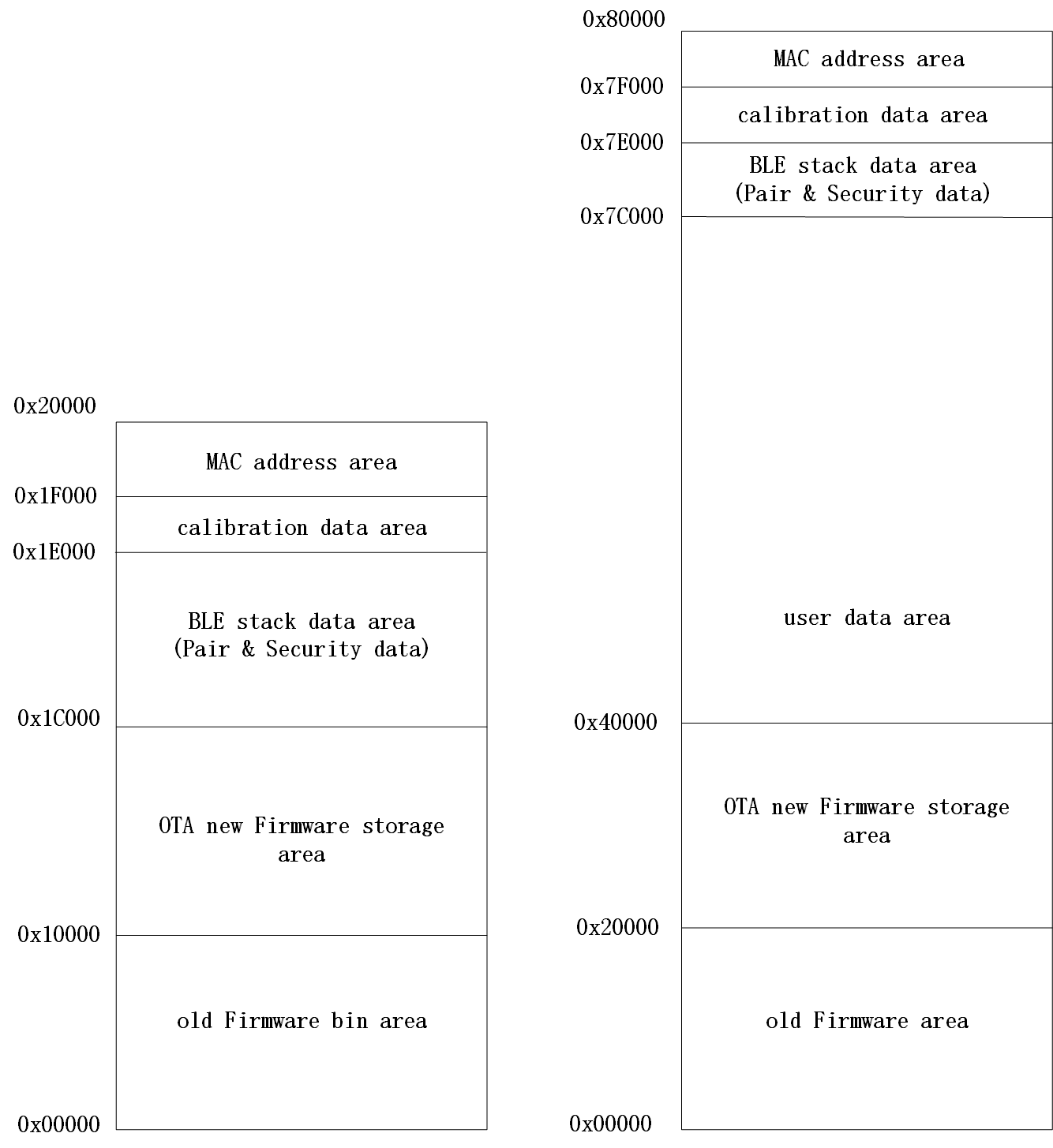
As shown in the figure above, all address assignments provide users with corresponding modification interfaces, and users can plan address assignments according to their needs. Users can define the following macro definitions according to the corresponding Flash size.
#define     FLASH_SIZE_OPTION_128K                 0x20000
#define     FLASH_SIZE_OPTION_512K                 0x80000

#define     FLASH_SIZE_OPTION                      FLASH_SIZE_OPTION_128K
(1) When using 512K Flash, the sector 0x7F000~0x80000 stores the MAC address. When using 128K Flash, it is 0x1F000~0x20000. In fact, the 6 bytes of MAC address are stored in 0x76000~0x76005 (0xFF000~0xFF005). In fact, the 6 bytes of MAC address are stored in 0x7F000\~0x7F005 (0x1F000\~0x1F005). When using 512K Flash, the high byte address is stored in 0x7F005, and the low byte address is stored in 0x7F000. For example, the contents of FLASH 0x7F000 to 0x7F005 are 0x11, 0x22, 0x33, 0x44, 0x55, 0x66, then the MAC address is 0x665544332211. Telink’s mass production fixture system will burn the actual product’s MAC address to 0x7F000 (0x1F000) address, which corresponds to the SDK. If the user needs to modify this address, please make sure that the address programmed by the fixture system is also modified accordingly. In the SDK, the MAC address will be read from the CFG_ADR_MAC of FLASH in the user_init function. This macro can be modified in stack/ble/blt_config.h.
/**************************** 512 K Flash *****************************/
#ifndef     CFG_ADR_MAC_512K_FLASH
#define     CFG_ADR_MAC_512K_FLASH                         0x7F000
#endif
/**************************** 128 K Flash *******************************/
#ifndef     CFG_ADR_MAC_128K_FLASH
#define     CFG_ADR_MAC_128K_FLASH                         0x1F000
#endif
(2) For the sector storage of 512K Flash 0x7E000~0x7EFFF, Telink MCU needs to calibrate the customized information, which is 0x1E000~0x1EFFF for 128K Flash. Only this part of the information does not follow the principle of "different types of information are placed in different sectors". Divide the 4096 bytes of this sector into different units for each 64 bytes, and each unit stores one type of calibration information. The calibration information can be placed in the same sector, because the calibration information is burned to the corresponding address during the fixture burning process. The actual firmware can only read the calibration information when it is running, and it is not allowed to write or erase it.
For details of calibration area information, please refer to "Telink_IC_Flash Customize Address_Spec". The calibration information is described with the offset address relative to the start address of the calibration area. For example, the offset address 0x00 refers to 0x7E000 or 0x1E000.
a) Offset address 0x00, 1 byte, stores the BLE RF frequency offset calibration value.
b) Offset address 0x40, 4 byte, stores the TP value calibration. B80 IC does not require TP calibration, which is ignored here.
c) Offset address 0xC0, stores the ADC Vref calibration value.
d) Offset address 0x180, 16 byte, stores the Firmware digital signature, which is used to prevent theft of the client Firmware.
e) Others, reserved.
(3) 512K Flash 0x7C000 ~ 0x7DFFF these two sectors are occupied by the BLE protocol stack system. For 128K Flash, they are 0x1C000~0x1DFFF, which are used to store pairing and encryption information. User can also modify the location of these two sectors. The size is fixed at two sectors 8K and cannot be modified. User can call the following function to modify the starting address of the paired encryption information storage:
void bls_smp_configParingSecurityInfoStorageAddr (int addr);
(4) For 512K Flash, the area of 0x00000 ~ 0x40000 is the program space, and for 128K Flash, it is 0x00000~0x0FFFF. Take 512K Flash as an example, 0x00000 ~ 0x1FFFF total 128K is Firmware storage space; 0x20000 ~ 0x3FFFF 128K is the space to store new Firmware when OTA update, i.e. the maximum Firmware space supported is 128K.
(5) All the remaining flash space is used as data storage space for USER.
Flash Operation
Flash space read/write operations use flash_read_page and flash_write_page functions, and flash erase uses flash_erase_sector function.
(1) Flash read/write operations
Flash read/write operations use flash_read_page and flash_write_page function pointers. which point to the flash_read_data and flash_page_program functions by default.
void flash_read_data(unsigned long addr, unsigned long len, unsigned char *buf);
void flash_page_program(unsigned long addr, unsigned long len, unsigned char *buf);
If needed, you can use the following API to change the read/write function of Flash:
void flash_change_rw_func(flash_hander_t read, flash_hander_t write);
The flash_read_page function reads the contents of the flash:
u8 data[6] = {0 };
flash_read_page(0x11000, 6, data); //读flash 0x11000开始的6个byte到data数组。
The flash_write_page function writes the flash:
u8 data[6] = {0x11,0x22,0x33,0x44,0x55,0x66 };
flash_write_page(0x12000, 6, data); //向flash 0x12000开始的6个byte写入0x665544332211。
The flash_write_page function is an operation on the page. A page in the flash is 256 byte. The maximum address size of this function operation is 256 byte, which cannot span two different page ranges.
When the operated address is the first address of a page, the maximum address is 256 byte, flash_write_page(0x12000, 256, data) is operated correctly, but flash_write_page(0x12000, 257, data) is wrong, because the last address does not belong to the page where 0x12000 is located anymore, the write operation will fail.
When the address being operated is not the first address of a page, pay more attention to the problem of cross-page. For example, flash_write_page (0x120f0, 20, data) is wrong. The first 16 addresses are in the page 0x12000, and the last 4 addresses are in the page 0x12100.
The flash_read_page does not have the cross-page problem mentioned above, and can read more than 256 bytes of data at one time.
Note:
- When using the flash_write_page function, user can only write up to 16 bytes at a time, more than that will cause a BLE interrupt exception.
- For the principle of this limitation, please refer to the introduction in the section "The Impact of Flash API on BLE Timing".
(2) flash erase operation
Use the flash_erase_sector function to erase the flash.
void flash_erase_sector(u32 addr);
A sector is 4096 byte, e.g. 0x13000 ~ 0x13fff is a complete sector.
addr must be the first address of a sector, and this function erases the entire sector each time.
It takes a long time to erase a sector. When the system clock is 16M, it takes about 30 ~ 100ms or even longer.
(3) Impact of flash read/write and erase operations on system interrupts
The three flash operation functions flash_read_page, flash_write_page, and flash_erase_sector introduced above must first turn off the system interrupt irq_disable() when executing, and then restore the interrupt irq_restore() after the operation is completed, the purpose of which is to ensure the integrity and continuity of the flash MSPI timing operation, and to prevent the reentry of hardware resources caused by another flash operation calling the MSPI bus in the interrupt.
The timing of the BLE SDK RF receiving and sending packets is all controlled by interrupts. The consequence of turning off the system interrupt during the flash operation is that the timing of BLE receiving and sending packets will be destroyed and no timely response.
The execution time of the flash_read_page function is not too long and has little impact on the interruption of BLE. When using flash_write_page, it is recommended to write up to 16 Bytes at a time when BLE is connected, if it is too long, it may affect the BLE timing. Therefore, it is strongly recommended that users do not continuously read and write too long addresses in the main_loop when BLE is connected.
The execution time of the flash_erase_sector function is tens to hundreds of ms, so in the main_loop of the main program, once the BLE connection state is entered, it is not allowed to call the flash_erase_sector function, otherwise it will destroy the time point of BLE receiving and sending packets, causing the connection to be disconnected. If it is unavoidable to erase the flash when BLE is connected, please follow the Conn state Slave role timing protection implementation method described later in this document to operate.
(4) Use pointer access to read flash
The firmware of the BLE SDK is stored on the flash, and when the program runs, only the first part of the flash is placed on the ram for execution as resident memory code, and the vast majority of the remaining code is read from the flash to the ram cache cache area (cache for short) when needed according to the program's locality principle. MCU reads the content on the flash by automatically controlling the internal MSPI hardware module.
User can use the pointer form to read the content on the flash. The principle of the pointer form to read the flash is that when the MCU system bus accesses the data, when it finds that the data address is not on the resident memory ramcode, the system bus will automatically switch to the MSPI, and the four lines MSCN, MCLK, MSDI and MSDO will operate the timing of the spi to get to read the flash data.
List three examples below:
u16  x = *(volatile u16*)0x10000; //读flash 0x10000两个byte
u8 data[16];
memcpy(data, 0x20000, 16);     //读flash 0x20000 16个byte copy到data
if(!memcmp(data, 0x30000, 16)){ //读flash 0x30000 16个byte和data比较
    ……
}
When reading the calibration value on the flash in user_init and setting it to the corresponding register, it is implemented by using pointers to access the flash. Please refer to the functions in the SDK.
static inline void blc_app_loadCustomizedParameters(void);
Read flash with pointer, but can't write flash with pointer (write flash can only be achieved by flash_write_page).
It should be noted that there is a problem with pointer read flash: as long as the data is read through the MCU system bus, the MCU will cache the data in the cache, if the data in the cache is not covered by other content, and there is a new request to access the data, the MCU will directly use the cached content in the cache as the result. If the following situation occurs in the user's code.
u8  result;
result = *(volatile u16*)0x40000;    //指针读取flash
u8 data = 0x5A;
flash_write_page(0x40000, 1, &data );
result = *(volatile u16*)0x40000;    //指针读取flash
if(result != 0x5A){  ..... }
The flash address 0x40000 was originally 0xff, the first read result is 0xff, then write 0x5A, theoretically the second read value is 0x5A, but the actual program gives the result is still 0xff, which was the first cache taken from the cache.
Note:
If this happens when the same address is read multiple times and the value of this address will be rewritten, do not use the pointer form, use API flash_read_page to achieve the safest, this function reads the result without taking the previously cached value from the cache.
It is correct to implement it as follows:
u8  result;
flash_read_page(0x40000, 1, &result );  //API 读取flash
u8 data = 0x5A;
flash_write_page(0x40000, 1, &data );
The position will be adaptively shifted to a later position of the flash according to the actual size of the flash.
Flash Operation Protection
Since the process of writing flash and erasing flash requires to transfer the address and data to flash through the SPI bus, the level stability on the SPI bus is very important. Any error in these critical data will cause irreversible consequences, such as writing the firmware wrong or erasing it by mistake will cause the firmware to no longer work and the OTA function will be disabled.
In the years of mass production experience of Telink chips, there have been errors caused by Flash operation under unstable conditions. Unstable conditions mainly include low power supply voltage, excessive power supply ripple, and intermittent power consumption of other modules on the system causing power supply jitter, and so on. In order to avoid similar operational risks in subsequent products, here we introduce some related Flash operation protection methods. After reading carefully, customers need to consider these issues as much as possible and add more security protection mechanisms to ensure product stability.
Low Voltage Detection Protection
Combine with the introduction of low power protection chapter, it is necessary to consider doing voltage detection before all Flash write and erase operations to avoid the situation of operating Flash at too low voltage. In addition, in order to ensure that the system is always working at a safe voltage, it is also recommended to do low voltage detection in main_loop at regular intervals to ensure the normal operation of the system.
Note:
About flash low-voltage protection, the following many places appear 2.0V, 2.2V and other thresholds, emphasize that these values are only examples, reference values. Customers have to assess the actual situation to modify these thresholds, such as single-layer boards, power supply fluctuations and other factors, are to improve the safety threshold as appropriate.
Take the low voltage detection in the SDK demo as an example:
Step 1: First, when powering on or waking up from deepsleep, before calling the Flash function, a low voltage test must be performed to prevent flash problems caused by low voltage:
void user_init_normal(void)
{

    ……

    #if (BATT_CHECK_ENABLE)
        u8 battery_check_returnVaule = 0;
        if(analog_read(USED_DEEP_ANA_REG) & LOW_BATT_FLG){
            battery_check_returnVaule = app_battery_power_check(VBAT_ALRAM_THRES_MV + 200);
        }
        else{
            battery_check_returnVaule = app_battery_power_check(VBAT_ALRAM_THRES_MV);
        }
        if(battery_check_returnVaule){
            ……
        }
        else{
            ……
        }
    #endif

    ……

}
Step 2: In the main_loop, low-voltage detection is required every 500ms:
if(battery_get_detect_enable() && clock_time_exceed(lowBattDet_tick, 500000) ){
    lowBattDet_tick = clock_time();
    u8 battery_check_returnVaule;
    if(analog_read(USED_DEEP_ANA_REG) & LOW_BATT_FLG){
        battery_check_returnVaule=app_battery_power_check(VBAT_ALRAM_THRES_MV + 200);
    }
    else{
        battery_check_returnVaule=app_battery_power_check(VBAT_ALRAM_THRES_MV);
    }
    if(battery_check_returnVaule){
        ……
    }
    else{
        ……
    }
}
Considering the working voltage of MCU and the working voltage of flash, if the Demo is set below 2.0V, the chip will directly enter deepsleep, and once the chip is detected to be lower than 2.0V, it needs to wait until the voltage rises to 2.2V, the chip will resume normal operation. Consider the following points in this design:
-
At 2.0V, when other modules are operated, the voltage may be pulled down and the flash will not work normally. Therefore, it is necessary to enter deepsleep below 2.0V to ensure that the chip no longer runs related modules;
-
When there is a low voltage situation, need to restore to 2.2V in order to make other functions normal, this is to ensure that the power supply voltage is confirmed in the charge and has a certain amount of power, then start to restore the function can be safer.
The above is the timing detection voltage and management method in SDK Demo, users can refer to it for design.
Note:
About flash low-voltage protection, the threshold values that appear above are only reference values. Customers have to assess the actual situation to modify these thresholds, such as single-layer boards, power supply fluctuations and other factors, are to improve the safety threshold as appropriate.
Flash Lock Protection
In addition to the above-mentioned timing voltage detection and management solutions, it is strongly recommended that customers do Flash erase and write protection.This is because in some cases, even if the low voltage detection result is safe, there is a small risk that the operation of each module in the application layer after the detection will cause the Flash power supply voltage to be pulled down, resulting in the Flash content being tampered when the Flash power supply voltage does not meet the conditions for real operation. Therefore, it is recommended that customers perform Flash erasing protection after the program is started, so that even if there is a misoperation, the content of the Flash will be more secure.
Generally, it is recommended that customers only write-protect the part of the program (the front part of Flash), so that the remaining Flash addresses can still be used for user-level data storage. Here we take the SDK Sample project as an example to describe how to calculate the protection size and the protection method.
Initialize Write Protection
(1) Calculate the protection size: Before initialization, calculate the size of the flash address to be write protected.
(2) Call flash_read_mid to determine the flash type, call the related function according to the result, and pass in the corresponding parameters according to the size to be protected. The relevant functions corresponding to the mid value can be found in the drivers/flash directory.
Protection Operations in the OTA Process
In OTA, because the flash needs to be erased and written, if there is a write-protected operation when power is on, it needs to be unlocked and protected during the OTA process. Flash unlock protection can be performed in the OTA_START callback, the steps are as follows:
Step 1: First, register the callback function in the initialization function as follows:
blc_ota_registerOtaStartCmdCb (&flash_ota_start);
Step 2: In the callback function, call the corresponding function to unlock the protection according to the flash type obtained before power-on:
void flash_ota_start(void)
{
switch(flash_lock_mid)
{
case mid value:
    corresponding unlock function;
    break;

        …
}
}
After the OTA ends, regardless of success or failure, the program will be re-run. Therefore, at the beginning of the program, the program will be write-protected again by the flash_lock method described in the previous section to form a closed loop to ensure the security of the application.
Internal Flash Introduction
Impact of Flash Access Timing on BLE Timing
Flash Access Timing
(1) Flash Operation Basic Timing

The figure above shows a typical MCU accessing Flash timing. During MSCN pull-down, the data interaction with Flash is completed through the level state change of MSDI and MSDO under the control of MCLK.
Flash access timing is the basic timing of Flash operations. The period of MSCN being pulled down is data interaction, and it ends after being pulled up. All Flash functions are based on it, and complex Flash functions can be divided into several basic sequence of Flash operations.
The basic timing of each Flash operation is relatively independent, and the next round of operations can only be performed after one operation timing is completed.
(2) MCU hardware access to Flash
Firmware is stored in Flash, and the MCU execution program needs to read instructions and data from Flash in advance. Combining with the introduction of section 2.1.2.1, we can see that the content that needs to be read is the text segment and the "read only data" segment. The MCU reads the instructions on the Flash in real time during the running process, so it will start the basic sequence of the Flash operation continuously. This process is automatically controlled by the MCU hardware and the software does not participate.
If an interrupt occurs during the main_loop program, it enters irq_handler. Even if the programs in main_loop and irq_handler are both in the text segment, there will be no Flash timing conflict because it is done by the MCU hardware, which will do the relevant arbitration and control work.
(3) Software access to Flash
MCU hardware access to Flash only solves the problem of reading program instructions and "read only data". If you need to manually read, write, and erase the Flash, use the flash_read_page, flash_write_page, flash_erase_sector and other APIs in the flash driver. Looking at the specific implementation of these APIs, it can be seen that the software controls the basic timing of Flash operations, first pulling down MSCN, then reading and writing data, and finally pulling up MSCN.
(4) Flash access timing conflicts and solutions
Since the basic timing of Flash operation is an indivisible and destructive process, when software and MCU hardware access Flash at the same time, there is a possibility of timing conflicts because software and MCU hardware do not have coordination and arbitration mechanisms.
The scenario where this timing conflict occurs is that the software calls flash_read_page, flash_write_page, flash_erase_sector and other APIs in main_loop, and when the MSCN is pulled low and data is being read or written, an interrupt occurs and some instructions in the irq_handler are stored in the text segment, the MCU hardware also starts a new basic timing for Flash operation, and this timing conflicts with the previous timing in main_loop, causing errors such as MCU crash.
As shown in the figure below, when Software access to Flash ends, an interrupt occurs and responds, and MCU hardware starts to access Flash. At this time, the result of Flash access will inevitably be wrong.
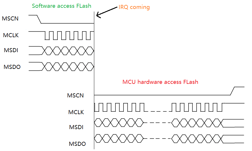
Analyzing the conditions that must be met at the same time for timing conflicts, it can be concluded that the methods for resolving the conflicts include the following:
a) Do not show any APIs for software manipulation of Flash timings in main_loop. this approach is not feasible and the use of APIs such as flash_write_page will appear on both the SDK and the application.
b) All procedures in the irq_handler function are stored in the ramcode in advance, without relying on any text segment or "read_only_data" segment. This method is not good either. It is limited by the Sram size of 8208 chips, if all the interrupt codes are stored in ramcode, the Sram resources are not enough. In addition, it is not easy to control this restriction for users, and it is not possible to ensure that the user interrupt code is written so tightly.
c) In the several APIs of the software operating Flash timing, add protection, close the interrupt, and prevent the irq_handler from responding. After the Flash access is over, the interrupt is resumed.
The Telink BLE SDK currently uses method 3, the Flash API to turn off interrupt protection. As shown in the code below (several codes are omitted in between), use irq_disable to turn off interrupts and irq_restore to restore them.
void flash_mspi_write_ram(unsigned char cmd, unsigned long addr, unsigned char addr_en, unsigned char *data, unsigned long data_len)
{
    unsigned char r = irq_disable();

    …… //flash access

    irq_restore(r);
}
The following diagram shows the principle of turning off the interrupt to protect the Flash access timing. The interrupt is turned off when the software accesses Flash, and the interrupt occurs in the middle but does not respond immediately (interrupt wait). When the software accesses Flash timing is all finished correctly, the interrupt is turned back on, and the interrupt responds immediately at this time, and then the MCU hardware accesses Flash.
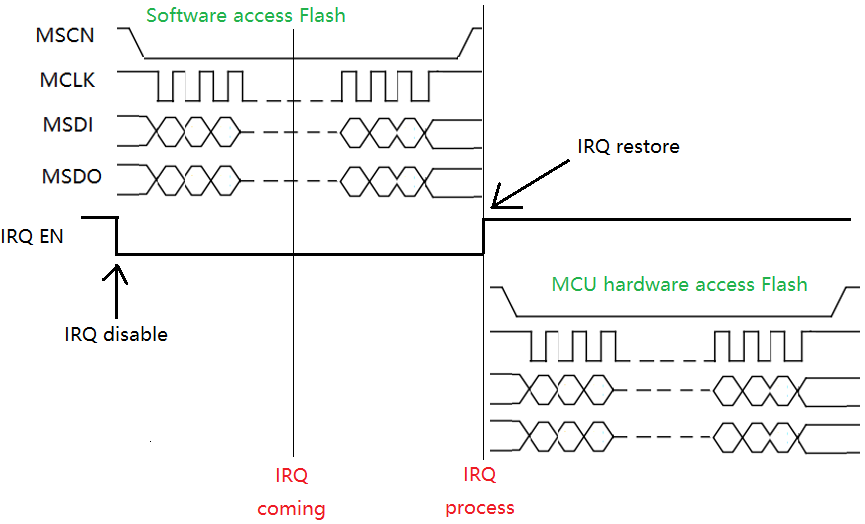
Impact of Flash API on BLE Timing
Previously introduced the use of Flash API to turn off the interrupt protection to solve the problem of timing conflicts between software and hardware MCU access to Flash. Since turning off the interrupt will make all interrupts unable to respond in real time, queuing to wait for the interrupt to resume and delay execution, you need to consider the possible side effects of the delayed time.
(1) Impact of off interrupt on BLE timing
Combine the characteristics of BLE timing to introduce. The BTX and BRX state machines in the BLE connection state in this SDK are all completed by interrupt tasks. BTX and BRX are similar implementations. Take BRX of slave role as an example.
The processing of BRX timing is more complicated. Take the processing of RX IRQ when more data appears in the BLE slave BRX as an example, as shown in the figure below. The SDK design requires the software to respond to every RX IRQ, which can be delayed but cannot be discarded. If a certain RX IRQ is lost, the RX packet that triggered this RX IRQ will also be lost, causing Linklayer packet loss errors.
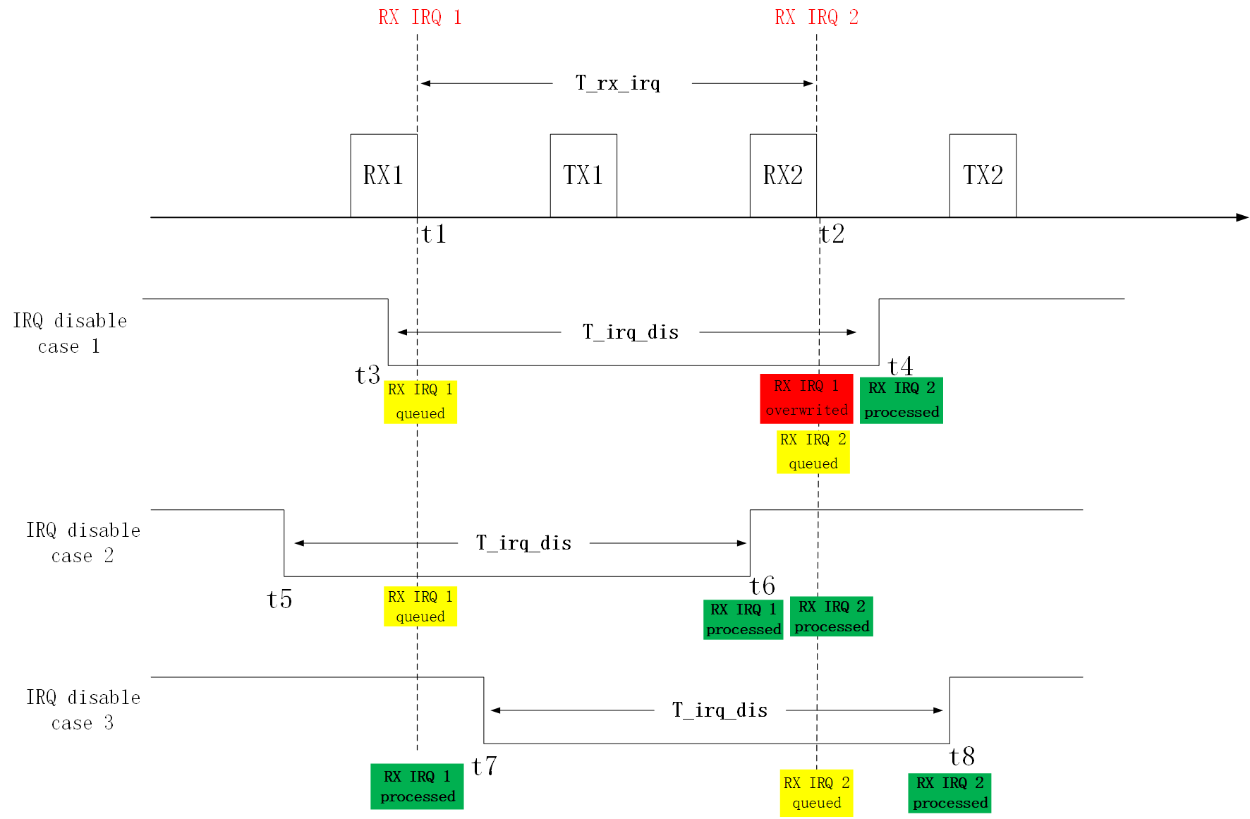
In the figure, RX1 triggers RX IRQ 1 at t1, and RX2 triggers RX IRQ 2 at t2. If no close interrupt occurs, the interrupt will respond in real time at t1 and t2, and the software correctly processes the RX packet.
The time difference between t1 and t2 is T_rx_irq, the off interrupt duration is T_irq_dis, T_irq_dis> T_rx_irq.
The off interrupt duration for all three cases IRQ disable case 1, IRQ disable case and IRQ disable case 3 is T_irq_dis, but the starting point of the off interrupt and the relative time of t1 are not the same.
IRQ disable case 1, t3 turns off the interrupt, t4 resumes the interrupt. t3 < t1; t4 > t2. RX IRQ 1 fails to respond at t1 and the interrupt is queued. RX IRQ 2 is triggered at t2, overwriting RX IRQ1 (because there can be only one RX IRQ in the interrupt wait queue), and RX IRQ 2 is queued and executed correctly at t4. RX IRQ 1 corresponding to RX1 is lost and Linklayer errors out if RX1 is a valid packet.
IRQ disable case 2 and IRQ disable case 3, RX IRQ 1 and RX IRQ 2 are delayed, but they are not lost and no error occurs.
An important conclusion can be drawn from the analysis of the above examples:
When the interrupt closing duration is greater than a certain safety threshold, there may be a risk of Linklayer error.
This safety threshold is related to the timing design of the Linklayer in the SDK and the timing characteristics of the BLE Spec. The T_rx_irq in the scale is much more complicated. The specific details will not be introduced in detail, and the safety threshold is directly given here as 220us.
The same is the off-interrupt duration T_irq_dis. In the above example, IRQ disable case 2 and IRQ disable case 3 are different. Because the off interrupt occurs at different time points, RX IRQ 1 or RX IRQ2 will be delayed in response, and RX IRQ 2 will not overwrite packet loss caused by RX IRQ1. Even with IRQ disable case 1, if RX1 and RX2 are irrelevant empty packets, packet loss will not cause any errors.
When the interrupt off duration is greater than 220us, it is not certain that an error will occur. Multiple conditions must be met at the same time to trigger an error. These conditions include: a long time to turn off the interrupt, and the time point of the RX IRQ occurrence match a specific relationship, more data appears in BTX or BRX, the two RX packets that continuously trigger RX IRQ are valid data packets rather than empty packets, and so on. So the final conclusion is:
There is a risk of linlayer errors when the interrupt off duration is greater than 220us, and the probability is very low.
The design of BLE SDK Linklayer aims at zero risk, that is, the interrupt closing duration is always less than 220us, and no chance of error is given.
Here is an additional introduction to the problem of RX packet loss in the above example. In the production of Telink BLE SDK, we often encounter this problem with customer feedback: under the premise that encryption is turned on, we see that the device sends a terminate packet with a reason of 0x3D (MIC_FAILURE), which leads to disconnection.
The above analysis shows that a long interrupt off time will cause the RX IRQ to be delayed for too long and then overwritten, and eventually lost packets. However, the SDK will handle the interrupt shutdown time correctly, which will be described in detail later in the document. The more likely reason is that the user uses other interrupts (such as Uart, USB, etc.), and the software execution time for these interrupts to respond is too long, which will have the same effect as the interrupt shutdown, and will also delay the RX IRQ. Here we limit the maximum safe time for a user interrupt execution to 100us.
(2) Impact of Flash API off interrupt protection on BLE timing
In order to avoid the timing conflict between software access to Flash and MCU hardware access to Flash, the Flash API uses a method of turning off interrupts. When the interrupt closing duration is greater than 220us, there is a risk of error in Linklayer. In order to solve the contradiction between the two, it is necessary to pay attention to the maximum time for the Flash API to close the interrupt.
The affected BLE timing is connection state slave role and master role. System initialization and Advertiisng state in mainloop are not affected. In the mainloop connection state, the following three Flash APIs are mainly concerned: flash_read_page, flash_write_page, flash_erase_sector. Other Flash APIs are generally not used or used during initialization.
a) flash_read_page
It has been tested and verified that when the number of bytes read by flash_read_page at a time does not exceed 64, the time is very safe, within 220us. After this value is exceeded, there will be a certain risk.
It is strongly recommended that users read up to 64 bytes when using flash_read_page to read Flash. If it exceeds 64 bytes, it needs to be split into multiple calls to flash_read_page to achieve.
b) flash_erase_sector
The time of flash_erase_sector is generally in the order of 10ms ~ 100ms, which is far more than 220us. So this SDK requires users not to call flash_erase_sector in the BLE connection state. If you call this API directly, the connection will definitely go wrong.
We recommend that users use other methods to replace the design of flash_erase_sector. For example, some applications are designed to repeatedly update some key information stored in Flash. In the design, you can consider selecting a larger area and using flash_write_page to continuously extend back.
For BLE slave applications, if the unavoidable flash_erase_sector occurs occasionally, you can use the Conn state Slave role timing protection mechanism to avoid it. Please refer to the details of this document.
Note that because the timing protection mechanism is very complicated, it is not recommended to use the high-frequency flash_erase_sector as it cannot guarantee the stability of the mechanism of repeated connection calls when the BLE slave is connected. It is recommended that users avoid this situation as much as possible by design.
c) flash_write_page
The flash_write_page time is affected by many key factors, including: Flash type, Flash technology, write byte number, high and low temperature, etc. The following is a detailed description from several types of internal Flash.
Use of Internal Flash API
According to the previous section, flash_write_page in Flash API is related to the type of internal Flash. This section describes in detail with several kinds of internal Flash already supported by 8208.
GD Flash
GD Flash belongs to the ETOX process.
The consumption time of flash_write_page is related to the parameter len (i.e. the number of bytes written at once), which is close to a positive relationship. After detailed testing and analysis within Telink, it is found that when the number of bytes is less than or equal to 16, the writing time can be stabilized within 220us; if the number of bytes exceeds 16, there will be risks.
For GD Flash, the maximum number of bytes written by flash_write_page is required to be 16. If it exceeds 16, such as 32, it can be split into two and write 16 bytes.
In the SDK design, there are two places involving flash_write_page. One is SMP storage configuration information, which uses 16 bytes per write; the other is when OTA writes new firmware, it also uses 16 bytes per write. In the design of OTA long package, for example, each package of 240 bytes of valid data is divided into 15 writes (16*15=240).
It is strongly recommended that customers use flash_write_page to write at most 16 bytes each time, otherwise there will be a risk of conflict with BLE timing.
Key Scan
Telink provides a keyscan architecture based on row/column scan to detect and process key state update (press/release). User can directly use the demo code, or realize the function by developing his own code.
Key Matrix
Figure shows a 2*2 Key matrix. Two drive pins (Row0, Row1) serve to output drive level, while two scan pins (CoL0, CoL1) serve to scan for key press in current column.
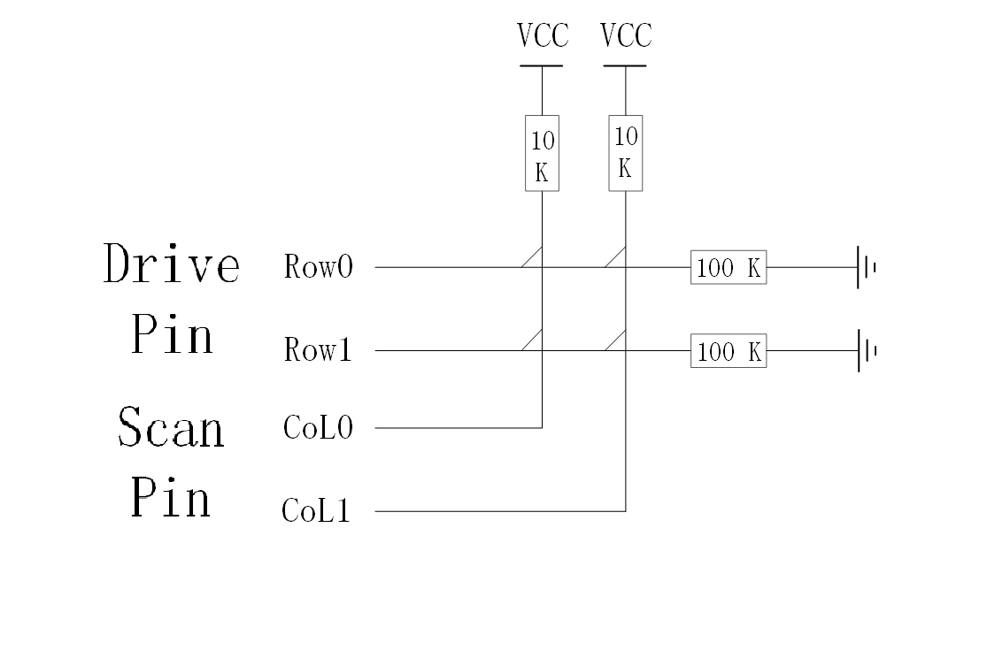
The Telink EVK board is a 2*2 keyboard matrix. In the actual product application, more keys may be needed, please add your own design. The following is an example of the onboard 2*2 matrix keyboard provided by Telink. Combined with the above figure, the keyscan related configuration in app_config.h is explained in detail as follows.
According to the real hardware circuit, on Telink EVK board, Row0 and Row1 pins are GPIO_PF0 and GPIO_PF1, CoL0 and CoL1 pins are GPIO_PA0 and GPIO_PD4.
Define drive pin array and scan pin array:
#define KB_DRIVE_PINS   {GPIO_PF0, GPIO_PF1}
#define KB_SCAN_PINS    {GPIO_PA0, GPIO_PD4}
Keyscan adopts analog pull-up/pull-down resistor of GPIO: drive pins use 100K pull-down resistor, and scan pins use 10K pull-up resistor. When no button is pressed, scan pins act as input GPIOs and read high level due to 10K pull-up resistor. When key scan starts, drive pins output low level; if low level is detected on a scan pin, it indicates there’s button pressed in current column (Note: Drive pins are not in float state, if output is not enabled, scan pins still detect high level due to voltage division of 100K and 10K resistor.)
Define valid voltage level detected on scan pins when drive pins output low level in Row/Column scan:
#define KB_LINE_HIGH_VALID 0
Define pull-up resistor for scan pins and pull-down resistor for drive pins:
#define MATRIX_ROW_PULL         PM_PIN_PULLDOWN_100K
#define MATRIX_COL_PULL         PM_PIN_PULLUP_10K
//drive pin need 100K pulldown
#define PULL_WAKEUP_SRC_PF0     MATRIX_ROW_PULL
#define PULL_WAKEUP_SRC_PF1     MATRIX_ROW_PULL
//scan  pin need 10K pullup
#define PULL_WAKEUP_SRC_PA0     MATRIX_COL_PULL
#define PULL_WAKEUP_SRC_PD4     MATRIX_COL_PULL
Since "ie" of general GPIOs is set as 0 by default in gpio_init, to read level on scan pins, corresponding "ie" should be enabled.
//drive pin open input to read gpio wakeup level
#define PF0_INPUT_ENABLE        1
#define PF1_INPUT_ENABLE        1
When MCU enters sleep mode, it’s needed to configure PAD GPIO wakeup. Set drive pins as high level wakeup; when there’s button pressed, drive pin reads high level, which is 10/11 VCC. To read level state of drive pins, corresponding "ie" should be enabled.
//scan pin open input to read gpio level
#define PA0_INPUT_ENABLE        1
#define PD4_INPUT_ENABLE        1
Keyscan and Keymap
Keyscan
After configuration as shown above, the function below is invoked in main_loop to implement keyscan.
u32 kb_scan_key (int numlock_status, int read_key)
numlock_status: Generally set as 0 when invoked in main_loop. Set as "KB_NUMLOCK_STATUS_POWERON" only for fast keyscan after wakeup from deepsleep (corresponding to DEEPBACK_FAST_KEYSCAN_ENABLE).
read_key: Buffer processing for key values, generally not used and set as 1 (if it’s set as 0, key values will be pushed into buffer and not reported to upper layer).
The return value is used to inform user whether matrix keyboard update is detected by current scan: if yes, return 1; otherwise return 0.
The "kb_scan_key" is invoked in main_loop. As in BLE timing sequence, each main_loop is an adv_interval or conn_interval. In advertising state (suppose adv_interval is 30ms), key scan is processed once for each 30ms; in connection state (suppose conn_interval is 10ms), key scan is processed once for each 10ms.
In theory, when button states in matrix are different during two adjacent key scans, it’s considered as an update.
In actual code, a debounce filtering processing is enabled: It will be considered as a valid update, only when button states stay the same during two adjacent key scans, but different with the latest stored matrix keyboard state. "1" will be returned by the function to indicate valid update, matrix keyboard state will be indicated by the structure "kb_event", and current button state will be updated to the newest matrix keyboard state. Corresponding code in keyboard.c is shown as below:
unsigned int key_debounce_filter( u32 mtrx_cur[], u32 filt_en );
The newest button state means press or release state set of all buttons in the matrix. When power on, initial matrix keyboard state shows all buttons are "released" by default, and debounce filtering processing is enabled. As long as valid update occurs to the button state, "1" will be returned, otherwise "0" will be returned.
For example: press a button, a valid update is returned; release a button, a valid update is returned; press another button with a button held, a valid update is returned; press the third button with two buttons held, a valid update is returned; release a button of the two pressed buttons, a valid update is returned……
Keymap & kb_event
If a valid button state update is detected by invoking the "kb_scan_key", user can obtain current button state via a global structure variable "kb_event".
#define KB_RETURN_KEY_MAX    6
typedef struct{
    u8 cnt;
    u8 ctrl_key;
    u8 keycode[KB_RETURN_KEY_MAX];
}kb_data_t;
kb_data_t   kb_event;
The "kb_event" consists of 8 bytes:
-
"cnt" serves to indicate valid count number of pressed buttons currently;
-
"ctrl_key" is not used generally except for standard USB HID keyboard (user is not allowed to set keycode in keymap as 0xe0~0xe7).
-
keycode[6] indicates keycode of up to six pressed buttons can be stored (if more than six buttons are pressed actually, only the former six can be reflected).
Keycode definition of all buttons in the "app_config.h" is shown as below:
#define     KB_MAP_NORMAL   {   {CR_VOL_UP,     VK_1},   \
                                {CR_VOL_DN,     VK_2}, }
The keymap follows the format of 2*2 matrix structure. The keycode of pressed button can be configured accordingly, for example, the keycode of the button at the cross of Row0 and CoL0 is "CR_VOL_UP".
In the "kb_scan_key" function, the "kb_event.cnt" will be cleared before each scan, while the array "kb_event.keycode[]" won’t be cleared automatically. Whenever "1" is returned to indicate valid update, the "kb_event.cnt" will be used to check current valid count number of pressed buttons.
a) If current kb_event.cnt = 0, previous valid matrix state "kb_event.cnt" must be uncertain non-zero value; the update must be button release, but the number of released button is uncertain. Data in kb_event.keycode[] (if available) is invalid.
b) If current kb_event.cnt = 1, the previous kb_event.cnt indicates button state update. If previous kb_event.cnt is 0, it indicates the update is one button is pressed; if previous kb_event.cnt is 2, it indicates the update is one of the two pressed buttons is released; if previous kb_event.cnt is 3, it indicates the update is two of the three pressed buttons are released……kb_event.keycode[0] indicates the key value of currently pressed button. The subsequent keycodes are negligible.
c) If current kb_event.cnt = 2, the previous kb_event.cnt indicates button state update. If previous kb_event.cnt is 0, it indicates the update is two buttons are pressed at the same time; if previous kb_event.cnt is 1, it indicates the update is another button is pressed with one button held; if previous kb_event.cnt is 3, it indicates the update is one of the three pressed buttons is released……kb_event.keycode[0] and kb_event.keycode[1] indicate key values of the two pressed buttons currently. The subsequent keycodes are negligible.
User can manually clear the "kb_event.keycode" before each key scan, so that it can be used to check whether valid update occurs, as shown in the example below.
In the sample code, when kb_event.keycode[0] is not zero, it’s considered a button is pressed, but the code won’t check further complex cases, such as whether two buttons are pressed at the same time or one of the two pressed buttons is released.
kb_event.keycode[0] = 0;//clear keycode[0]
int det_key = kb_scan_key (0, 1);
if (det_key)
{
    key_not_released = 1;
    u8 key0 = kb_event.keycode[0];
    if (kb_event.cnt == 2)   //two key press, do  not process
    {
    }
    else if(kb_event.cnt == 1)
    {
key_buf[2] = key0;
         //send key press
        bls_att_pushNotifyData (HID_NORMAL_KB_REPORT_INPUT_DP_H, key_buf, 8);
}
    else  //key release
    {
        key_not_released = 0;
        key_buf[2] = 0;
        //send key release
        bls_att_pushNotifyData (HID_NORMAL_KB_REPORT_INPUT_DP_H, key_buf, 8);
    }
}
Keyscan Flow
When "kb_scan_key" is invoked, a basic keyscan flow is shown as below:
(1) Initial full scan through the whole matrix.
All drive pins output drive level (0). Meanwhile read all scan pins, check for valid level, and record the column on which valid level is read. (The scan_pin_need is used to mark valid column number.)
If row-by-row scan is directly adopted without initial full scan through the whole matrix, each time all rows should be scanned at least, even if no button is pressed. To save scan time, initial full scan through the whole matrix can be added, thus it will directly exit keyscan if no button press is detected on any column.
The first full scan codes:
scan_pin_need = kb_key_pressed (gpio);
In the "kb_key_pressed" function, all rows output low level, and stabilized level of scan pins will be read after 20us delay. A release_cnt is set as 6; if a detection shows all pressed buttons in the matrix are released, it won’t consider no button is pressed and stop row-by-row scan immediately, but buffers for six frames. If six successive detections show buttons are all released, it will stop row-by-row scan. Thus key debounce processing is realized.
(2) Scan row by row according to full scan result through the whole matrix.
If button press is detected by full scan, row-by-row scan is started: Drive pins (ROW0,ROW1) output valid drive level row by row; read level on columns, and find the pressed button. Following is related code:
u32 pressed_matrix[ARRAY_SIZE(drive_pins)] = {0};
kb_scan_row (0, gpio);
for (int i=0; i<=ARRAY_SIZE(drive_pins); i++) {
    u32 r = kb_scan_row (i < ARRAY_SIZE(drive_pins) ? i : 0, gpio);
    if (i) {
        pressed_matrix[i - 1] = r;
    }
}
The following methods are used to optimize code execution time for row-by-row scan.
-
When a row outputs drive level, it’s not needed to read level of all columns (CoL0,CoL1). Since the scan_pin_need marks valid column number, user can read the marked columns only.
-
After a row outputs drive level, a 20us or so delay is needed to read stabilized level of scan pins, and a buffer processing is used to utilize the waiting duration.
The array variable "u32 pressed_matrix[5]" (up to 40 columns are supported) is used to store final matrix keyboard state: pressed_matrix[0] bit0~bit2 mark button state on CoL0~CoL2 crossed with Row0, ……, pressed_matrix[4] bit0~bit5 mark button state on CoL0~CoL2 crossed with Row4.
(3) Debounce filtering for pressed_matrix[].
Corresponding codes:
unsigned int key_debounce_filter( u32 mtrx_cur[], u32 filt_en );
u32 key_changed = key_debounce_filter( pressed_matrix, (numlock_status & KB_NUMLOCK_STATUS_POWERON) ? 0 : 1);
During fast keyscan after wakeup from deepsleep, "numlock_status" equals "KB_NUMLOCK_STATUS_POWERON"; the "filt_en" is set as 0 to skip filtering and fast obtain key values.
In other cases, the "filt_en" is set as 1 to enable filtering. Only when pressed_matrix[] stays the same during two adjacent key scans, but different from the latest valid pressed_matrix[], will the "key_changed" set as 1 to indicate valid update in matrix keyboard.
(4) Buffer processing for pressed_matrix[].
Push pressed_matrix[] into buffer. When the "read_key" in "kb_scan_key (int numlock_status, int read_key)" is set as 1, the data in the buffer will be read out immediately. When the "read_key" is set as 0, the buffer stores the data without notification to the upper layer; the buffered data won’t be read until the read_key is 1.
In current SDK, the "read_key" is fixed as 1, i.e. the buffer does not take effect actually.
(5) According to pressed_matrix[], look up the KB_MAP_NORMAL table and return key values.
Corresponding functions are "kb_remap_key_code" and "kb_remap_key_row".
Software Timer
Telink BLE SDK supplies source code of blt software timer demo for user reference on timer task. User can directly use this timer or modify as needed.
The source code are available in "vendor/common/blt_soft_timer.c" and "blt_soft_timer.h". To use this timer, first change the macro FEATURE_TEST_MODE to TEST_USER_BLT_SOFT_TIMER in feature_config.h:.
#define FEATURE_TEST_MODE TEST_USER_BLT_SOFT_TIMER
Since blt software timer is inquiry timer based on system tick, it cannot reach the accuracy of hardware timer, and it should be continuously inquired during main_loop.
The blt soft timer applies to the use scenarios with timing value more than 5ms and without high requirement for time error.
Its key feature is: This timer will be inquired during main_loop, and it ensures MCU can wake up in time from suspend and execute timer task. This design is implemented based on "Timer wakeup by Application layer" (section 4.5 Timer wakeup by Application Layer).
The current design can run up to four timers, and maximum timer number is modifiable via the macro below:
#define MAX_TIMER_NUM 4 //timer max number
Timer Initialization
The API below is used for blt software timer initialization:
void blt_soft_timer_init(void);
Timer initialization only registers "blt_soft_timer_process" as callback function of APP layer wakeup in advance.
void  blt_soft_timer_init(void){
      bls_pm_registerAppWakeupLowPowerCb(blt_soft_timer_process);
}
Timer Inquiry Processing
The function "blt_soft_timer_process" serves to implement inquiry processing of blt software timer.
void blt_soft_timer_process(int type);
On one hand, main_loop should always invoke this function in the location as shown in the figure below. On the other hand, this function must be registered as callback function of APP layer wakeup in advance. Whenever MCU is woke up from suspend in advance by timer, this function will be quickly executed to process timer task.
void main_loop (void)
{
    blt_soft_timer_process(MAINLOOP_ENTRY);
    blc_sdk_main_loop();
    #if (UI_KEYBOARD_ENABLE)
        proc_keyboard (0, 0, 0);
    #endif
    blt_pm_proc();
}
The parameter "type" of the "blt_soft_timer_process" indicates two cases to enter this function: If "type" is 0, it indicates entering this function via inquiry in main_loop; if "type" is 1, it indicates entering this function when MCU is woke up in advance by timer.
#define     MAIN_LOOP_ENTRY               0
#define     CALLBACK_ENTRY                1
The implementation of the "blt_soft_timer_process" is rather complex, and its basic principle is shown as below:
(1) First check whether there is still user-defined timer in current timer table. If not, directly exit the function and disable timer wakeup of APP layer; if there’s timer task, continue the flow.
if(!blt_timer.currentNum){
    bls_pm_setAppWakeupLowPower(0, 0);  //disable
    return;
}
(2) Check whether the nearest timer task is reached: if the task is not reached, exit the function; otherwise continue the flow. Since the design will ensure all timers are time-ordered, herein it’s only needed to check the nearest timer.
if( !blt_is_timer_expired(blt_timer.timer[0].t, now) ){
    return;
}
(3) Inquire all current timer tasks, and execute corresponding task as long as timer value is reached.
for(int i=0; i<blt_timer.currentNum; i++){
if(blt_is_timer_expired(blt_timer.timer[i].t ,now) ){ //timer trigger
    if(blt_timer.timer[i].cb == NULL){
    }
    else{
        result = blt_timer.timer[i].cb();
        if(result < 0){
            blt_soft_timer_delete_by_index(i);
        }
        else if(result == 0){
            change_flg = 1;
            blt_timer.timer[i].t = now + blt_timer.timer[i].interval;
        }
        else{  //set new timer interval
            change_flg = 1;
            blt_timer.timer[i].interval = result * CLOCK_16M_SYS_TIMER_CLK_1US;
            blt_timer.timer[i].t = now + blt_timer.timer[i].interval;
            }
        }
    }
}
The code above shows processing of timer task function: If the return value of this function is less than 0, this timer task will be deleted and won’t be responded; if the return value is 0, the previous timing value will be retained; if the return value is more than 0, this return value will be used as the new timing cycle (unit: us).
(4) In step 3, if tasks in timer task table change, the previous time sequence may be disturbed, and re-ordering is needed.
if(change_flg){
    blt_soft_timer_sort();
}
(5) If the nearest timer task will be responded within 3s (it can be changed to a value larger than 3s as needed) from now, the response time will be set as wakeup time by APP layer in advance; otherwise APP layer wakeup in advance will be disabled.
if( (u32)(blt_timer.timer[0].t - now) < 3000 *  CLOCK_16M_SYS_TIMER_CLK_1MS){
    bls_pm_setAppWakeupLowPower(blt_timer.timer[0].t,  1);
}
else{
    bls_pm_setAppWakeupLowPower(0, 0);  //disable
}
Add Timer Task
The API below serves to add timer task.
typedef int (*blt_timer_callback_t)(void);
int     blt_soft_timer_add(blt_timer_callback_t func, u32 interval_us);
"func": timer task function.
"interval_us": timing value (unit: us).
The int-type return value corresponds to three processing methods:
(1) If the return value is less than 0, this task will be automatically deleted after execution. This feature can be used to control the number of timer execution times.
(2) If the return value is 0, the old interval_us will be used as timing cycle.
(3) If the return value is more than 0, this return value will be used as new timing cycle (unit: us).
int blt_soft_timer_add(blt_timer_callback_t func, u32 interval_us)
{
    int i;
    u32 now = clock_time();
    if(blt_timer.currentNum >= MAX_TIMER_NUM){  //timer full
        return  0;
    }
    else{
        blt_timer.timer[blt_timer.currentNum].cb = func;
        blt_timer.timer[blt_timer.currentNum].interval = interval_us * CLOCK_16M_SYS_TIMER_CLK_1US;
        blt_timer.timer[blt_timer.currentNum].t = now + blt_timer.timer[blt_timer.currentNum].interval;
        blt_timer.currentNum ++;
        blt_soft_timer_sort();
        bls_pm_setAppWakeupLowPower(blt_timer.timer[0].t,  1);
        return  1;
    }
}
As shown in the implementation code, if timer number exceeds the maximum value, the adding operation will fail. Whenever a new timer task is added, re-ordering must be implemented to ensure timer tasks are time-ordered, while the index corresponding to the nearest timer task should be 0.
Delete Timer Task
As introduced above, timer task will be automatically deleted when the return value is less than 0. Except for this case, the API below can be invoked to specify the timer task to be deleted.
int blt_soft_timer_delete(blt_timer_callback_t func);
Demo
For Demo code of blt soft timer, please refer to "feature_soft_timer" in feature_test.
int gpio_test0(void)
{
    DBG_CHN3_TOGGLE;
    return 0;
}
static u8 timer_change_flg = 0;
int gpio_test1(void)
{
    DBG_CHN4_TOGGLE;
    timer_change_flg = !timer_change_flg;
    if(timer_change_flg){
        return 7000;
    }
    else{
        return 17000;
    }
}
int gpio_test2(void)
{
    DBG_CHN5_TOGGLE;
    if(clock_time_exceed(0, 5000000)){
        //return  -1;
        blt_soft_timer_delete(&gpio_test2);
    }
    return 0;
}
int gpio_test3(void)
{
    DBG_CHN6_TOGGLE;
    return 0;
}
Initialization:
blt_soft_timer_init();
blt_soft_timer_add(&gpio_test0, 23000);//23ms
blt_soft_timer_add(&gpio_test1, 7000); //7ms <-> 17ms
blt_soft_timer_add(&gpio_test2, 13000);//13ms
blt_soft_timer_add(&gpio_test3, 27000);//27ms
Four timer tasks are defined with different features:
(1) gpio_test0: Toggle once for every 23ms.
(2) gpio_test1: Switch between two timers of 7ms/17ms.
(3) gpio_test2: Delete itself after 5s, which can be implemented by invoking "blt_soft_timer_delete(&gpio_test2)" or "return -1".
(4) gpio_test3: Toggle once for every 27ms.
Software UART
In order to facilitate some users' dual UART tasks, in addition to supporting hardware UART, B80 BLE SDK also provides blt software UART demo, and all source code is provided. Users can use it directly after understanding the design ideas of the demo, or they can make some modifications to the design themselves.
The source code is all in the files drivers -> ext_driver -> software_uart.c and software_uart.h. If you need to use it, first change the macro FEATURE_TEST_MODE to TEST_USER_BLT_SOFT_UART in feature_config.h:
#define FEATURE_TEST_MODE TEST_USER_BLT_SOFT_UART
The blt soft uart TX is designed based on polling and is only allowed to transmit between the broadcast time and the connection time interval. The blt soft uart RX is designed based on gpio interrupt and timer interrupt.
Note:
To reduce interrupt processing task time, the software serial projects must use SYS_CLK_48M_Crystal.
Software UART Initialization
Call the following API to initialize:
soft_uart_rx_handler(app_soft_rx_uart_cb);
soft_uart_RxSetFifo(uart_rx_fifo.p, uart_rx_fifo.size);
soft_uart_init();
It can be seen that the soft_uart_rx_handler function registers the UART RX handler function in the irq handler as the callback function app_soft_rx_uart_cb defined by the application layer.
int app_soft_rx_uart_cb(void)//UART data send to Master,we will handler the data as CMD or DATA
{
    if (((uart_rx_fifo.wptr - uart_rx_fifo.rptr) & 255) < uart_rx_fifo.num) {
        uart_rx_fifo.wptr++;
        unsigned char* p = uart_rx_fifo.p + (uart_rx_fifo.wptr & (uart_rx_fifo.num - 1)) * uart_rx_fifo.size;
        soft_uart_RxSetFifo(p, uart_rx_fifo.size);
    }
    return 0;
}
The soft_uart_RxSetFifo function registers the UART receive FIFO as the defined uart_rx_fifo of the upper layer.
u8          uart_rx_buf[80 * 4] = {0};
my_fifo_t   uart_rx_fifo = {
    80,
    4,
    0,
    0,
    uart_rx_buf,};
The soft_uart_init function initializes the GPIO ports used by the software UART RX and TX, the RX GPIO interrupt, the variables related to the software UART, and the used timer0.
void soft_uart_init(void)
{

    // set software rx io
    gpio_set_func(SOFT_UART_RX_IO, AS_GPIO);
    gpio_set_output_en(SOFT_UART_RX_IO, 0);
    gpio_set_input_en(SOFT_UART_RX_IO, 1);
    gpio_setup_up_down_resistor(SOFT_UART_RX_IO, PM_PIN_PULLUP_10K);
    gpio_set_interrupt(SOFT_UART_RX_IO, POL_FALLING);

    //set software tx io
    gpio_set_func(SOFT_UART_TX_IO , AS_GPIO);
    gpio_setup_up_down_resistor(SOFT_UART_TX_IO, PM_PIN_PULLUP_1M);
    gpio_set_output_en(SOFT_UART_TX_IO,1);//Enable output
    gpio_write(SOFT_UART_TX_IO, 1);// Add this code to fix the problem that the first byte will be error.

    soft_uart_rece.bit_num = 0x00;
    soft_uart_rece.temp_byte = 0x00;

    soft_uart_rece.stop_count = 0;
    soft_uart_rece.done_count = 0;

    soft_uart_rece.state = SOFT_UART_WAIT;

    soft_uart_rece.mutex_flag = 0;

    soft_uart_rece.time_interval = (1000000 / SOFT_UART_BAUD_RATE) * CLOCK_SYS_CLOCK_1US + SOFT_UART_OFFSET;
    //SET TIME
    timer0_set_mode(TIMER_MODE_SYSCLK, 0, SOFT_UART_INTERVAL * CLOCK_SYS_CLOCK_1US);
    timer_stop(TIMER0);
}
Software UART TX Processing
The blt software UART TX processing is implemented using the soft_uart_send function. Users can refer to the demo of the analog serial port only sending data, the configuration is as follows.
#define    TEST_RX_TX_RUN                     1
#define    TEST_ONLY_TX_RUN                   2

#define    TEST_SOFT_UART_RUN_MODEL           TEST_ONLY_TX_RUN
Call the soft_uart_send function in the main_loop as shown in the figure below to process each timer task.
u8 send_buf[10] = {0xaa,0x55,0xaa,0x55,0xaa,0x55,0xaa,0x55,0xaa,0x55};

void main_loop (void)
{
    ...
    soft_uart_send(send_buf, 10);
    ...
}
The 10 Byte of data sent can be seen through the serial port host computer tool. In addition, an external logic analyzer can also see the results.

The specific implementation ideas of blt software UART TX are as follows:
(1) First, send data by Byte, and check the current state of the state machine before sending. If the current state is advertising, go to (2); if the current state is connection, go to (3); if the current state is standby, go to (4).
void soft_uart_send(unsigned char * buf, unsigned char len) {

    unsigned char i;
    for (i = 0; i < len; i++) {

        unsigned char s;
        extern u8 blc_ll_getCurrentState(void);
        s = blc_ll_getCurrentState();
        ...
    }

}
(2) The current state is advertising state, call blc_sdk_adv to check whether the broadcast time has been reached, if so, send the broadcast first, then allow TX, and jump to (4).
void soft_uart_send(unsigned char * buf, unsigned char len) {
    ...
    /*
    #define     BLS_LINK_STATE_ADV                 BIT(0)
    */
    if (s == BIT(0)) {
        extern void blc_sdk_adv(void);
        blc_sdk_adv();
    }
    ...
}
(3) The current state is connection state, call blc_ll_SoftUartisRfState to check whether the current RF task affects the TX task, if the current moment to the next connection event is greater than the UART TX a Byte data time (SOFT_UART_SEND_ONE_BYTE), allow TX, jump to (4), otherwise need to wait for the end of the next connection event.
void soft_uart_send(unsigned char * buf, unsigned char len) {
    ...
    /*
    #define         BLS_LINK_STATE_CONN                 BIT(3)
    */
    if (s == BIT(3)) {
        extern void blc_ll_SoftUartisRfState(int acl_margin_us);
        blc_ll_SoftUartisRfState(SOFT_UART_SEND_ONE_BYTE);
    }
    ...
}
(4) In the case of allowing UART TX, call the soft_uart_putchar function to send the i-th Byte.
void soft_uart_send(unsigned char * buf, unsigned char len) {
    ...
    soft_uart_putchar(buf[i]);
    ...
}
Software UART RX Processing
The blt software UART RX processing is implemented using gpio interrupt and timer interrupt, RX actions are performed in irq handler. Users can refer to the demo of the analog serial port sending and receiving data, the configuration is as follows.
#define    TEST_RX_TX_RUN                           1
#define    TEST_ONLY_TX_RUN                         2

#define    TEST_SOFT_UART_RUN_MODEL                 TEST_RX_TX_RUN
In main_loop as shown in the following position to process the received RX data and TX back again through the soft_uart_send function.
void main_loop (void)
{
    ...
    if (uart_rx_fifo.wptr != uart_rx_fifo.rptr) {
        u8 *p = uart_rx_fifo.p + (uart_rx_fifo.rptr & (uart_rx_fifo.num - 1))
                * uart_rx_fifo.size;

        soft_uart_send(&p[4], p[0]);

        uart_rx_fifo.rptr++;
    }
    ...
}
Send 10 Byte data through the serial port host computer tool, you can receive the data sent back by the host computer in the receiving window. In addition, an external logic analyzer can also see the effect.

The specific implementation ideas of blt software UART RX are as follows:
(1) Firstly, GPIO irq will be triggered when the data sent by the host computer is received. If the software uart state is SOFT_UART_WAIT, GPIO irq will be turned off and the interrupt will be triggered by setting the timer irq tick to read the GPIO input value at the next RX interval and set the current software uart state to SOFT_UART_WORK.
_attribute_ram_code_ void soft_uart_irq_handler(void)
{
    ...
    if ((reg_irq_src & FLD_IRQ_GPIO_EN) == FLD_IRQ_GPIO_EN) {
        reg_irq_src |= FLD_IRQ_GPIO_EN; // clear the relevant irq
        if ((gpio_read(SOFT_UART_RX_IO) == 0)&&(SOFT_UART_WAIT & soft_uart_rece.state)) {
                BM_CLR(reg_gpio_irq_wakeup_en(SOFT_UART_RX_IO), SOFT_UART_RX_IO & 0xff); // close GPIO irq
                soft_uart_rece.bit_num = 0x00;
                soft_uart_rece.temp_byte = 0x00;
                soft_uart_rece.state &= ~SOFT_UART_DONE_CHECK;
                soft_uart_rece.state &= ~SOFT_UART_WAIT;
                soft_uart_rece.state |= SOFT_UART_WORK;
                soft_uart_rece.done_count = 0;
                timer0_set_mode(TIMER_MODE_SYSCLK, 0, soft_uart_rece.time_interval);
                timer_start(TIMER0);
        }
    }
    ...
}
(2) When the timer irq is triggered, clear the timer irq status, after that judge the current software uart state and perform the corresponding operation. If the state is SOFT_UART_WORK, jump to (3); if the state is SOFT_UART_STOP_CHECK, jump to (4); if the state is SOFT_UART_DONE_CHECK, jump to (5).
_attribute_ram_code_ void soft_uart_irq_handler(void)
{
...
//time irq
if (timer_get_interrupt_status(FLD_TMR_STA_TMR0)) {
timer_clear_interrupt_status(FLD_TMR_STA_TMR0); //clear irq status
if (soft_uart_rece.state & SOFT_UART_WORK) {
...
} else if (soft_uart_rece.state & SOFT_UART_STOP_CHECK) {
...
} else if (soft_uart_rece.state & SOFT_UART_DONE_CHECK) {
...
}
}
...
}
(3) The software uart state is SOFT_UART_WORK, temporarily store the current bit value, if 8-bit value has been received, set software uart state to SOFT_UART_STOP_CHECK.
_attribute_ram_code_ void soft_uart_irq_handler(void)
{
...
if (soft_uart_rece.state & SOFT_UART_WORK) {
if (1 == gpio_read(SOFT_UART_RX_IO)) { //
soft_uart_rece.temp_byte |= BIT(soft_uart_rece.bit_num);
}
soft_uart_rece.bit_num++;
if (8 == soft_uart_rece.bit_num) {
soft_uart_rece.bit_num = 0x00;
soft_uart_rece.state |= SOFT_UART_STOP_CHECK; //change state
soft_uart_rece.state &= ~SOFT_UART_WORK;
}
}
...
}
(4) The software uart state is SOFT_UART_STOP_CHECK, save the previously transferred Byte value, then set the software uart state to SOFT_UART_DONE_CHECK and SOFT_UART_WAIT, and call soft_uart_RxHandler to do some processing and reopen the RX GPIO irq.
_attribute_ram_code_ void soft_uart_irq_handler(void)
{
...
if (soft_uart_rece.state & SOFT_UART_STOP_CHECK) {
soft_uart_rece.state &= ~SOFT_UART_STOP_CHECK;
if (1 == gpio_read(SOFT_UART_RX_IO)) { //
soft_uart_rece.data[soft_uart_rece.data_count + 4] = soft_uart_rece.temp_byte; //len + buf
soft_uart_rece.temp_byte = 0x00;
soft_uart_rece.data_count++;
if (soft_uart_rece.data_count >= soft_uart_rece.data_size) { //over flow
soft_uart_rece.data[0] = soft_uart_rece.data_count;
if (soft_uart_RxHandler)
soft_uart_RxHandler();
}
}
soft_uart_rece.state |= SOFT_UART_DONE_CHECK;
soft_uart_rece.state |= SOFT_UART_WAIT;
reg_irq_src |= FLD_IRQ_GPIO_EN; // clear the relevant irq
BM_SET(reg_gpio_irq_wakeup_en(SOFT_UART_RX_IO), SOFT_UART_RX_IO & 0xff); //start io irq
}
...
}
(5) The software uart state is SOFT_UART_DONE_CHECK, clear SOFT_UART_DONE_CHECK state and call soft_uart_RxHandler to do some processing and turn off timer irq.
_attribute_ram_code_ void soft_uart_irq_handler(void)
{
...
if (soft_uart_rece.state & SOFT_UART_DONE_CHECK) {
soft_uart_rece.done_count++;
if (UART_RECE_DONE_NUM <= soft_uart_rece.done_count) {
timer_stop(TIMER0);
if(soft_uart_rece.data_count > 0){
soft_uart_rece.data[0] = soft_uart_rece.data_count;
if (soft_uart_RxHandler)
soft_uart_RxHandler();
}
soft_uart_rece.state &= ~SOFT_UART_DONE_CHECK;
}
}
...
}
Feature Demo Introduction
B80_feature_test provides demo codes for some commonly used BLE-related features. Users can refer to these demos to complete their own function implementation. See code for details. Select the macro "FEATURE_TEST_MODE" in app_config.h in the B80_feature_test to switch to the demo of different feature test.
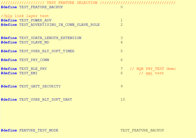
Test methods of each demo are described below.
Broadcast Power Consumption Test
This item mainly tests the power consumption during broadcasting of different broadcasting parameters. Users can measure the power consumption with an external multimeter during the test. Need to modify FEATURE_TEST_MODE to TEST_POWER_ADV in app_config.h.
#define FEATURE_TEST_MODE TEST_POWER_ADV
Modify the broadcast type and broadcast parameters in feature_adv_power as required. There are two types of broadcasts provided in app_config.h: connectable broadcast and un-connectable broadcast.
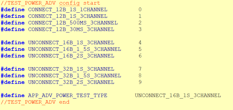
Connectable Broadcast Power Consumption Test
In feature_adv_power, the following codes belong to the connectable broadcast type.
#define CONNECT_12B_1S_1CHANNEL 0
#define CONNECT_12B_1S_3CHANNEL 1
#define CONNECT_12B_500MS_3CHANNEL 2
#define CONNECT_12B_30MS_3CHANNEL 3
The default broadcast data length of Demo is 12 bytes, and users can modify it according to their needs.
//ADV data length: 12 byte
u8 tbl_advData[12] = {0x08, 0x09, 't', 'e', 's', 't', 'a', 'd', 'v',0x02, 0x01, 0x05,};
The Demo provides 1s_1channel,1s_3channel,500ms_3channel,30ms_3channel broadcast parameters, users can select the corresponding test items according to their needs.
Un-connectable Broadcast Power Consumption Test
In feature_adv_power, the following codes belong to the un-connectable broadcast type.
#define UNCONNECT_16B_1S_3CHANNEL 4
#define UNCONNECT_16B_1_5S_3CHANNEL 5
#define UNCONNECT_16B_2S_3CHANNEL 6
#define UNCONNECT_31B_1S_3CHANNEL 7
#define UNCONNECT_31B_1_5S_3CHANNEL 8
#define UNCONNECT_31B_2S_3CHANNEL 9
The Demo provides two broadcast data lengths of 16byte and 31byte, which users can choose according to their needs.
u8 tbl_advData[] = {
15, 0x09, 't', 'e', 's', 't', 'a', 'd', 'v', '8', '9', 'A', 'B', 'C', 'D', 'E',
};//ADV data length: 16 byte
u8 tbl_advData[] = {
30, 0x09, 't', 'e', 's', 't', 'a', 'd', 'v', '8', '9', 'A', 'B', 'C', 'D', 'E', 'F', '0', '1', '2', '3', '4', '5', '6', '7', '8', '9', 'A', 'B', 'C', 'D'
};//ADV data length: max 31 byte
The Demo provides 1s3channel, 1.5s3channel, and 2s3channel broadcast parameters. Users can select the corresponding test items according to their needs.
GATT Security Test
The user needs to change FEATURE_TEST_MODE to TEST_GATT_SECURITY in feature_config.h.
#define FEATURE_TEST_MODE TEST_GATT_SECURITY
As known from the BLE module ATT&GATT chapter, each Attribute in the service list defines read and write permissions, that is, the pairing mode must reach the corresponding level to read or write. For example, in the SPP service of Demo:
// client to server RX
{0,ATT_PERMISSIONS_READ,2,sizeof(TelinkSppDataClient2ServerCharVal),(u8*)(&my_characterUUID), (u8*)(TelinkSppDataClient2ServerCharVal), 0}, //prop
{0,SPP_C2S_ATT_PERMISSIONS_RDWR,16,sizeof(SppDataClient2ServerData),(u8*)(&TelinkSppDataClient2ServerUUID), (u8*)(SppDataClient2ServerData), &module_onReceiveData}, //value
{0,ATT_PERMISSIONS_READ,2,sizeof(TelinkSPPC2SDescriptor),(u8*)&userdesc_UUID,(u8*)(&TelinkSPPC2SDescriptor)},
The read and write permissions of the second Attribute are defined as: SPP_C2S_ATT_PERMISSIONS_RDWR.
This read and write permission is up to the user to choose, you can choose one of the following:
#define SPP_C2S_ATT_PERMISSIONS_RDWR ATT_PERMISSIONS_RDWR
#define SPP_C2S_ATT_PERMISSIONS_RDWR ATT_PERMISSIONS_ENCRYPT_RDWR
#define SPP_C2S_ATT_PERMISSIONS_RDWR ATT_PERMISSIONS_AUTHEN_RDWR
#define SPP_C2S_ATT_PERMISSIONS_RDWR ATT_PERMISSIONS_SECURE_CONN_RDWR
No matter which one you choose, the current pairing mode must be higher than or equal to this level of read and write permissions to read and write services correctly.
GATT test mainly tests the process of pairing encryption, mainly divided into the following ways:
-
LE_Security_Mode_1_Level_1, no authentication and no encryption.
-
LE_Security_Mode_1_Level_2, unauthenticated paring with encryption.
-
LE_Security_Mode_1_Level_3, authenticated paring with encryption-legacy.
-
LE_Security_Mode_1_Level_4, authenticated paring with encryption-sc.
The user needs to select app_config.h according to the needs of the corresponding pairing mode.
// LE security mode select
#define SMP_TEST_MODE LE_SECURITY_MODE_1_LEVEL_1
Below is a brief introduction to each pairing mode.
LE_Security_Mode_1_Level_1
// LE_Security_Mode_1_Level_1, no authentication and no encryption
#define SMP_TEST_NO_SECURITY 1
LE_Security_Mode_1_Level_1 is the simplest pairing method, neither authentication nor encryption. The user changes the LE_SECURITY_MODE_1_LEVEL_1 of app_config.h to SMP_TEST_NO_SECURITY.
#define LE_SECURITY_MODE_1_LEVEL_1 SMP_TEST_NO_SECURITY
Change SMP_TEST_MODE to LE_SECURITY_MODE_1_LEVEL_1.
#define SMP_TEST_MODE LE_SECURITY_MODE_1_LEVEL_1
LE_Security_Mode_1_Level_2
// LE_Security_Mode_1_Level_2, unauthenticated pairing with encryption
#define SMP_TEST_LEGACY_PAIRING_JUST_WORKS 2 //JustWorks
#define SMP_TEST_SC_PAIRING_JUST_WORKS 3 //JustWorks
The LE_Security_Mode_1_Level_2 mode is just work, only encryption but not authentication. Just work is divided into legacy just work and sc just work. In the GATT Security test, LE_SECURITY_MODE_1_LEVEL_2 in app_config.h defaults to SMP_TEST_LEGACY_PARING_JUST_WORKS. SMP_TEST_SC_PARING_JUST_WORKS is not processed, and users can configure it according to the API. SMP_TEST_LEGACY_PARING_JUST_WORKS is described below.
SMP_TEST_LEGACY_PARING_JUST_WORKS
The user makes the following modifications:
#define LE_SECURITY_MODE_1_LEVEL_2 SMP_TEST_LEGACY_PARING_JUST_WORKS
#define SMP_TEST_MODE LE_SECURITY_MODE_1_LEVEL_2
The process is shown as following:
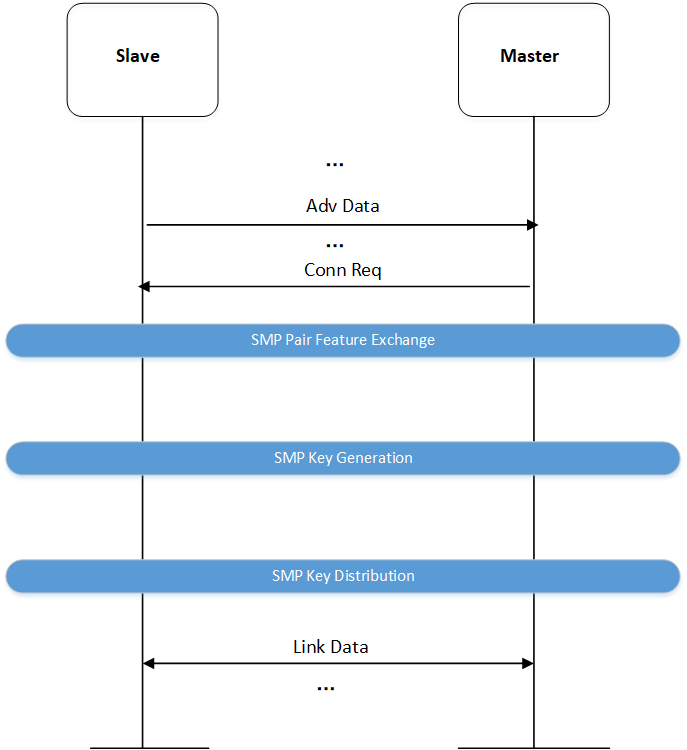
LE_Security_Mode_1_Level_3
// LE_Security_Mode_1_Level_3, authenticated pairing with encryption
#define SMP_TEST_LEGACY_PASSKEY_ENTRY_SDMI 4 //PK_Resp_Dsply_Init_Input
#define SMP_TEST_LEGACY_PASSKEY_ENTRY_MDSI 5 //PK_Init_Dsply_Resp_Input
#define SMP_TEST_LEGACY_PASSKEY_ENTRY_MISI 6 //PK_BOTH_INPUT, not test
#define SMP_TEST_LEGACY_PASSKEY_ENTRY_OOB 7 //OOB_Authentication, not test
LE_Security_Mode_1_Level_3 is both the authentication and encryption Legacy pairing method. According to the pairing parameter settings, it is divided into OOB, PassKey Entry, and Numeric Comparison. Currently the demo provides sample codes SMP_TEST_LEGACY_PASSKEY_ENTRY_SDMI only. The method is briefly introduced below.
SMP_TEST_LEGACY_PASSKEY_ENTRY_SDMI
The user needs to modify as follows in app_config.h:
#define LE_SECURITY_MODE_1_LEVEL_3 SMP_TEST_LEGACY_PASSKEY_ENTRY_SDMI
#define SMP_TEST_MODE LE_SECURITY_MODE_1_LEVEL_3
During the pairing process, the slave side needs to display the key and the master side enters the key. During initialization, a gap event related to pairing is registered. The pairing information will be notified to the app layer.
blc_gap_registerHostEventHandler( app_host_event_callback );
blc_gap_setEventMask( GAP_EVT_MASK_SMP_PAIRING_BEGIN | \
GAP_EVT_MASK_SMP_PAIRING_SUCCESS | \
GAP_EVT_MASK_SMP_PAIRING_FAIL | \
GAP_EVT_MASK_SMP_TK_DISPALY | \
GAP_EVT_MASK_SMP_CONN_ENCRYPTION_DONE | \
GAP_EVT_MASK_SMP_SECURITY_PROCESS_DONE);
The user needs to print the current key information when receiving the GAP_EVT_SMP_TK_DISPALY.
int app_host_event_callback (u32 h, u8 *para, int n)
{
u8 event = h & 0xFF;
switch(event)
{
…
case GAP_EVT_SMP_TK_DISPALY:
{
char pc[7];
u32 pinCode = *(u32*)para;
sprintf(pc, "%d", pinCode);
printf("TK display:%s\n", pc);
}
…
}
}
The process is shown as following:
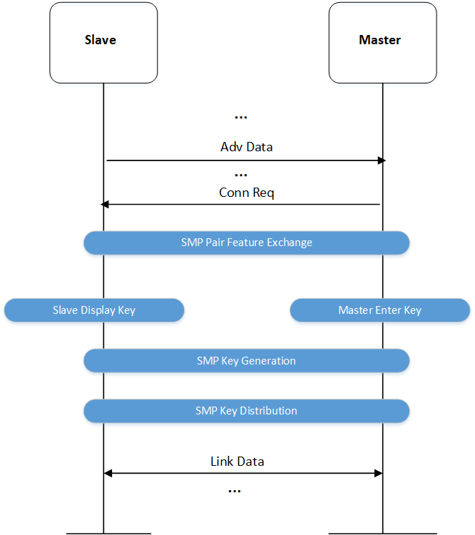
LE_Security_Mode_1_Level_4
// LE_Security_Mode_1_Level_4, authenticated pairing with encryption
#define SMP_TEST_SC_NUMERIC_COMPARISON 8 //Numric_Comparison
#define SMP_TEST_SC_PASSKEY_ENTRY_SDMI 9 //PK_Resp_Dsply_Init_Input
#define SMP_TEST_SC_PASSKEY_ENTRY_MDSI 10//PK_Init_Dsply_Resp_Input
#define SMP_TEST_SC_PASSKEY_ENTRY_MISI 11//PK_BOTH_INPUT, not test
#define SMP_TEST_SC_PASSKEY_ENTRY_OOB 12//OOB_Authentication, not test
LE_Security_Mode_1_Level_4 is both an authentication and encryption SC pairing method. According to the pairing parameter settings, it is divided into OOB, PassKey Entry, and Numeric Comparison. Currently the demo provides sample codes SMP_TEST_SC_PASSKEY_ENTRY_SDMI only. The method is briefly introduced below.
SMP_TEST_SC_PASSKEY_ENTRY_SDMI
The user needs to modify as follows in feature_security.c:
#define LE_SECURITY_MODE_1_LEVEL_4 SMP_TEST_SC_PASSKEY_ENTRY_SDMI
#define SMP_TEST_MODE LE_SECURITY_MODE_1_LEVEL_4
During the pairing process, the slave side needs to display the key and the master side enters the key. During initialization, a gap event related to pairing is registered. The pairing information will be notified to the app layer.
blc_gap_registerHostEventHandler( app_host_event_callback );
blc_gap_setEventMask( GAP_EVT_MASK_SMP_PAIRING_BEGIN | \
GAP_EVT_MASK_SMP_PAIRING_SUCCESS | \
GAP_EVT_MASK_SMP_PAIRING_FAIL | \
GAP_EVT_MASK_SMP_TK_DISPALY | \
GAP_EVT_MASK_SMP_CONN_ENCRYPTION_DONE | \
GAP_EVT_MASK_SMP_SECURITY_PROCESS_DONE);
The user needs to print the current key information when receiving the GAP_EVT_MASK_SMP_TK_DISPLAY message.
int app_host_event_callback (u32 h, u8 *para, int n)
{
u8 event = h & 0xFF;
switch(event)
{
…
case GAP_EVT_SMP_TK_DISPALY:
{
char pc[7];
u32 pinCode = *(u32*)para;
sprintf(pc, "%d", pinCode);
printf("TK display:%s\n", pc);
}
break;
…
}
}
The process is shown as following:
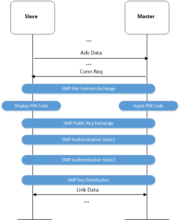
GATT Security Test Process
For example, the current pairing mode is LE_SECURITY_MODE_1_LEVEL_3, that is, there are both authentication and encryption Legacy pairing modes. So the current read and write permissions can be selected as follows.
#define SPP_C2S_ATT_PERMISSIONS_RDWR ATT_PERMISSIONS_AUTHEN_RDWR
The process is shown as following:
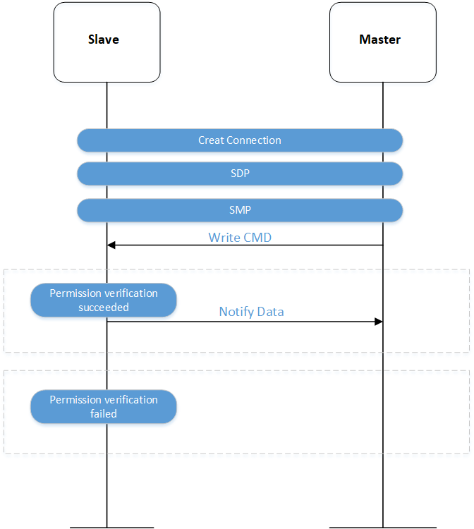
DLE Test
The DLE test mainly tests the long package. For the corresponding feature_config.h selection, the code is as follows:
#define FEATURE_TEST_MODE TEST_SDATA_LENGTH_EXTENSION
After programming, press reset, B80 as the slave side chooses to establish a connection with the master. After the connection is successful, the MTU and DataLength are exchanged.
blc_att_requestMtuSizeExchange(BLS_CONN_HANDLE, MTU_SIZE_SETTING);
blc_ll_exchangeDataLength(0x14 , ACL_CONN_MAX_TX_OCTETS);//LENGTH_REQ opcode: 0x14
After the exchange is successful, the slave will send a long packet of data to the master every 3.3s.
The test process is as follows:
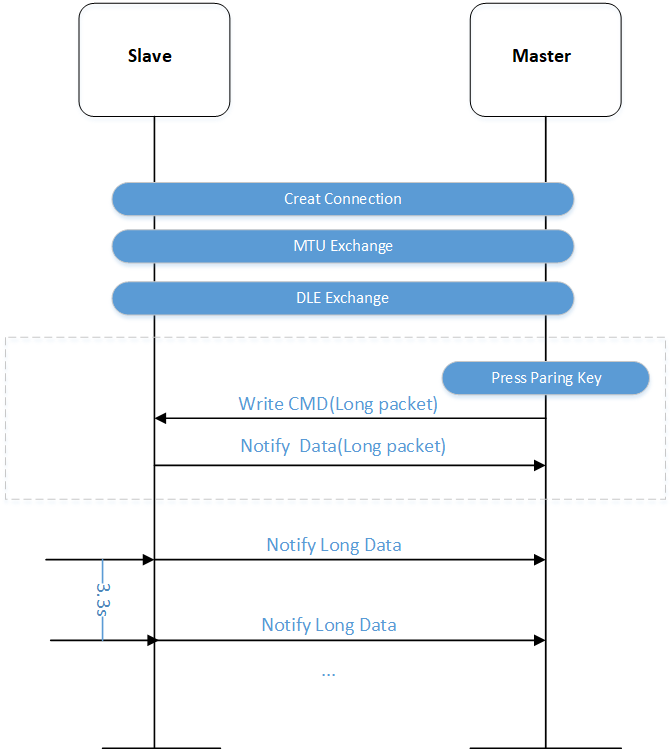
Note:
Note that when deepsleep retention is turned on, if the RX FIFO size and TX FIFO size are set to more than 200, there may not be enough ram, and the user needs to evaluate and modify.
Soft Timer Test
Please refer to the chapter of Software Timer.
EMI Test
The feature_emi is used to generate the required EMI test signals. This routine needs to be used with the EMI_Tool and "Non_Signaling_Test_Tool" tools.
Protocol
Please refer to "Telink SoC EMI Test User Guide" for the communication protocol.
Demo Introduction
EMI test in B80 supports carrieronly mode, continue mode, burst mode, and packet receiving mode.
Supported wireless communication methods include Ble1M, Ble2M, Ble125K, Ble500K, Zigbee250K.
For the introduction of each mode and functional function, users can refer to "Telink Driver SDK Developer Handbook".
Other Modules
24MHz Crystal External Capacitor
Refer to the position C3/C4 of the 24MHz crystal matching capacitor in the figure below.
The SDK defaults to use B80 internal capacitance (that is, the cap corresponding to ana_8a\<5:0>) as the matching capacitance of the 24MHz crystal oscillator. At this time, C3/C4 does not need to be soldered. The advantage of using this solution is that the capacitance can be measured and adjusted on the Telink fixture to make the frequency value of the final application product reach the best.
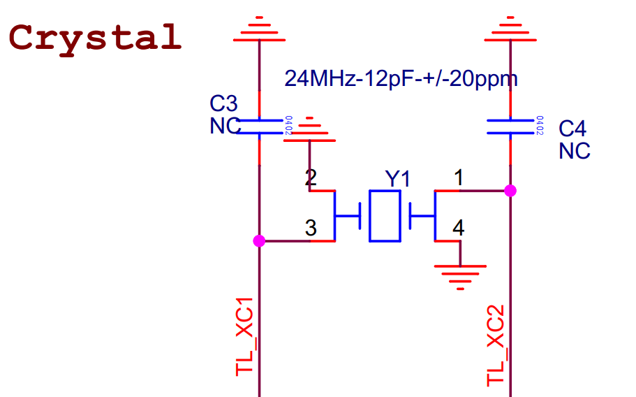
If you need to use an external welding capacitor as the matching capacitor (C3/C4 welding capacitor) of the 24MHz crystal oscillator, just call the following API at the beginning of the main function (must be before the blc_app_loadCustomizedParameters() function and after the cpu_wakeup_init function):
static inline void blc_app_setExternalCrystalCapEnable(u8 en)
{
blt_miscParam.ext_cap_en = en;
}
As long as the API is called before cpu_wakeup_init, the SDK will automatically handle all the settings, including disabling the internal matching capacitor, no longer reading the frequency bias correction value, etc.
32KHz Clock Source Selection
The SDK supports the use of either the MCU's internal 32k RC oscillator circuit (referred to as 32k RC) or an external 32k RC oscillator circuit (referred to as 32k Pad). The error of 32k RC is relatively large, so for applications with long suspend or deep retention time, the time accuracy will be worse. At present, the maximum long connection supported by 32k RC by default cannot exceed 3s. Once exceeding this time, ble_timing will have errors, resulting in inaccurate packet receiving time points, prone to receiving and sending packets retry, increased power consumption, and even disconnection. The error is much smaller when using the 32k Pad.
The user only needs to call the following API at the beginning of the main function (must be before the cpu_wakeup_init function):
Call 32k RC:
void blc_pm_select_internal_32k_crystal(void);
Call 32k Pad:
void blc_pm_select_external_32k_crystal (void);
Firmware Digital Signature
There is a method of malicious copying of products in the market. For example, if customer A develops a product using Telink's chip and SDK, customer A's competitor customer B, who also uses Telink's chip, gets the product and can copy the same hardware circuit design. If the product's data burn-in bus is not disabled, it is possible for customer B to read the complete firmware on the product's Flash, and customer B can copy the product using the same hardware and software.
To address these security risks, the SDK supports a software digital signature function. The principle is to take advantage of the fact that the chip's internal Flash has a unique UID. The product reads the 16 byte UID from the internal Flash during the fixture burn-in process and then performs a complex encryption operation with the contents of the Firmware to produce a set of checksum values called Signature, which are stored at the corresponding address in the Flash calibration area. Which is:
Signature = Encryption_function (Firmware, Flash_UID)
Signature is related to both Firmware and Flash_UID. The same calculation is done when the program is initialized on the SDK, the result is compared with the Signature burned on the fixture and if it does not match, the program is not legal and is prohibited from running.
It is important to emphasize that this feature involves a number of technical aspects, including the fitment of the jig, the corresponding configuration on the SDK, etc. Customers must confirm the details with Telink FAE in advance if required.
Below are some technical details of the implementation of this feature.
(1) The jig end must be correctly matched, including file configuration, writing scripts, etc. Please refer to the Telink testbench documentation and instructions for details.
(2) The Signature memory address is the Flash Calibration area offset address 0x180 continuous 16 byte.
(3) This feature is disabled by default on the SDK, to use it, enable the following macro in app_config.h.
#define FIRMWARES_SIGNATURE_ENABLE 1 //firmware check
Note:
There are only a few projects on the SDK that add Firmware digital signature verification to the initialization of the main function (see FIRMWARES_SIGNATURE_ENABLE by searching for it). If the customer is using a project that does not have this feature, please make sure to merge from another project to your own.
The code in the SDK is shown below and the program needs to be disabled when the digital signature does not match. The SDK uses the simplest while(1) to disable the program when the digital signature does not match, this is just a sample writeup, please evaluate for yourself if this method meets the requirements, if not you can use other methods such as putting the MCU into deepsleep, modifying various data, bss, stack segments etc. stack segments, etc.
void blt_firmware_signature_check(void)
{
unsigned int flash_mid;
unsigned char flash_uid[16];
unsigned char signature_enc_key[16];
int flag = flash_read_mid_uid_with_check(&flash_mid, flash_uid);
if(flag==0){ //reading flash UID error
while(1);
}
firmware_encrypt_based_on_uid (flash_uid, signature_enc_key);
//signature not match
if(memcmp(signature_enc_key, (u8*)(flash_sector_calibration + CALIB_OFFSET_FIRMWARE_SIGNKEY), 16)){
while(1); //user can change the code here to stop firmware running
}
}
(4) The calculation method for the digital signature, Encryption_function, is defined by Telink and takes into account both the Firmware content and the Flash_UID, using AES 128 encryption. The details of the calculation are not publicly available and are packaged in a sealed library. The above firmware_encrypt_based_on_uid function is implemented in libfirmware_encrypt.a.
If customers feel that the generic encryption algorithm is not secure enough and need to use their own encryption algorithm, they can contact Telink FAE to discuss the solution.
SDK Version
The function for obtaining version information has been added to facilitate users to obtain the version information of the current SDK and library.
unsigned char blc_get_sdk_version(unsigned char *pbuf,unsigned char number);
Users should get at least 5 bytes when calling this interface, the first 5 bytes show the SDK version, and the rest are reserved for the future.
For example, if the number you get after calling this API is {3,4,0,0,1}, it means the SDK version is 3.4.0.0 Patch 1.
Debug
Introduction to GPIO Simulation UART_TX Printing Method
To facilitate the user to print information when debugging, B80 supports gpio simulation printing printf(const char *format, ...),sprintf(char *buff, const char *format, ...), the relevant information needs to be defined in drivers/printf.h as follows.
#define DEBUG_MODE 1
#define DEBUG_BUS 1
#if(DEBUG_BUS==DEBUG_IO)
#define PRINT_BAUD_RATE 115200 //1M baud rate,should Not bigger than 1Mb/s
#define DEBUG_INFO_TX_PIN GPIO_PD3
#define TX_PIN_GPIO_EN() gpio_set_func(DEBUG_INFO_TX_PIN , AS_GPIO);
#define TX_PIN_PULLUP_1M() gpio_setup_up_down_resistor(DEBUG_INFO_TX_PIN, PM_PIN_PULLUP_1M);
#define TX_PIN_OUTPUT_EN() gpio_set_output_en(DEBUG_INFO_TX_PIN,1)
#define TX_PIN_OUTPUT_REG (0x503+((DEBUG_INFO_TX_PIN>>8)<<3))
#endif
The default baud rate here is 115200 and the TX_PIN is GPIO_PD3, the user can change the baud rate and TX_PIN according to the actual needs.
If the user wants to use a higher baud rate (greater than 115200, maximum support 1M), the user needs to increase the cclk, at least to 24MHz or more, change the cclk in app_config.h.
/////////////////// Clock /////////////////////////////////
/**
* @brief MCU system clock
*/
#define CLOCK_SYS_CLOCK_HZ 24000000
Note:
The information printed by printf may be interrupted by a garbled message, do not print in an interrupt!
Q&A
Q.How to create my own project in the SDK?
A.Generally, to ensure that the various settings in the project are in place, we usually build new projects based on a particular demo. For example, we use 8208_ble_sample as a base to complete a new project.
Step 1: Copy and paste the code and rename it. As shown below, we copy the code for 8208_ble_sample and newly name it Test_Demo.
Step 2: Right-click on the project, Properties -> Settings –> Manage Configurations, create a new project, for example: Test_Demo.
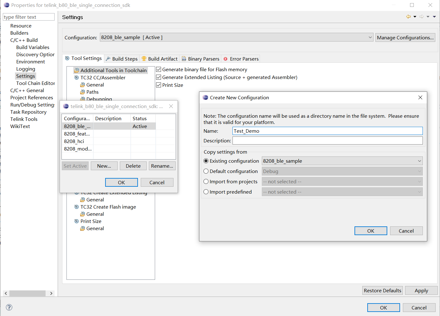
After clicking OK, you can see the new project in the project list, as shown below.
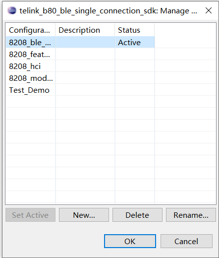
Step 3: Right-click on the Test_Demo folder, Resource Configurations -> Exclude from Build, tick all the items in Test_Demo's settings except for itself. And tick Test_Demo in the same settings for its copy source. This is shown as below.
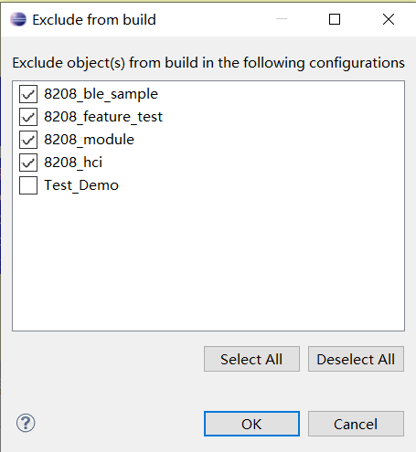
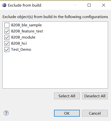
Step 4: Change the Setting-TC32 Compiler-symbols in the Test_Demo property to the new symbols and click Apply after the change, as shown below:
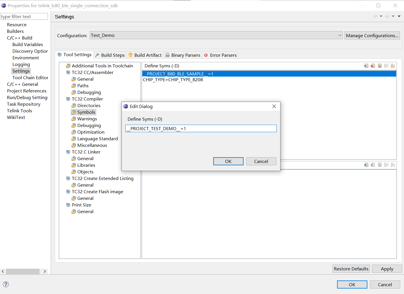
Step 5: In vender/common/user_config.h, add corresponding to the settings for the new code. As shown below:
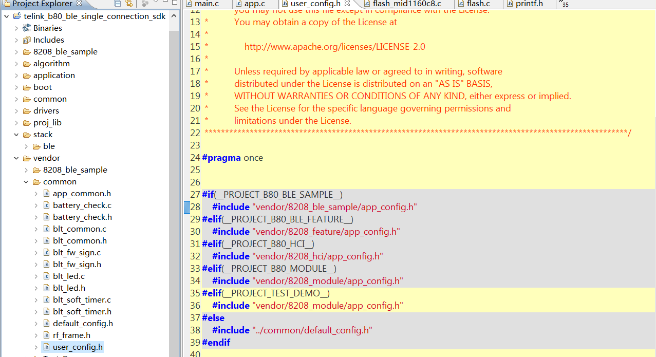
At this point, the new project has been built. You can now select the new project, clean it and build it for use.
Appendix
crc16 Algorithm
unsigned short crc16 (unsigned char *pD, int len)
{
static unsigned short poly[2]={0, 0xa001};
unsigned short crc = 0xffff;
unsigned char ds;
int i,j;
for(j=len; j>0; j--)
{
unsigned char ds = *pD++;
for(i=0; i<8; i++)
{
crc = (crc >> 1) ^ poly[(crc ^ ds ) & 1];
ds = ds >> 1;
}
}
return crc;
}