Telink Live Mic SDK Developer Handbook
Quick Start Guide
Overview
Document Purpose
Complete description of common SDK configuration, use and debugging methods, for users to quickly get started, and solve most of the problems encountered in the actual development process.
Glossary of Terms
TBD
Hardware Related
Hardware Block Diagrams
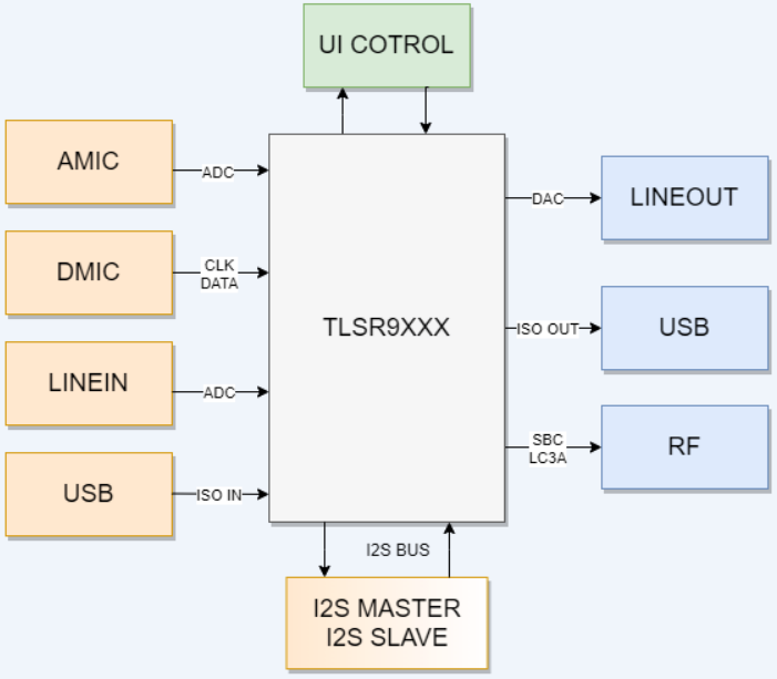
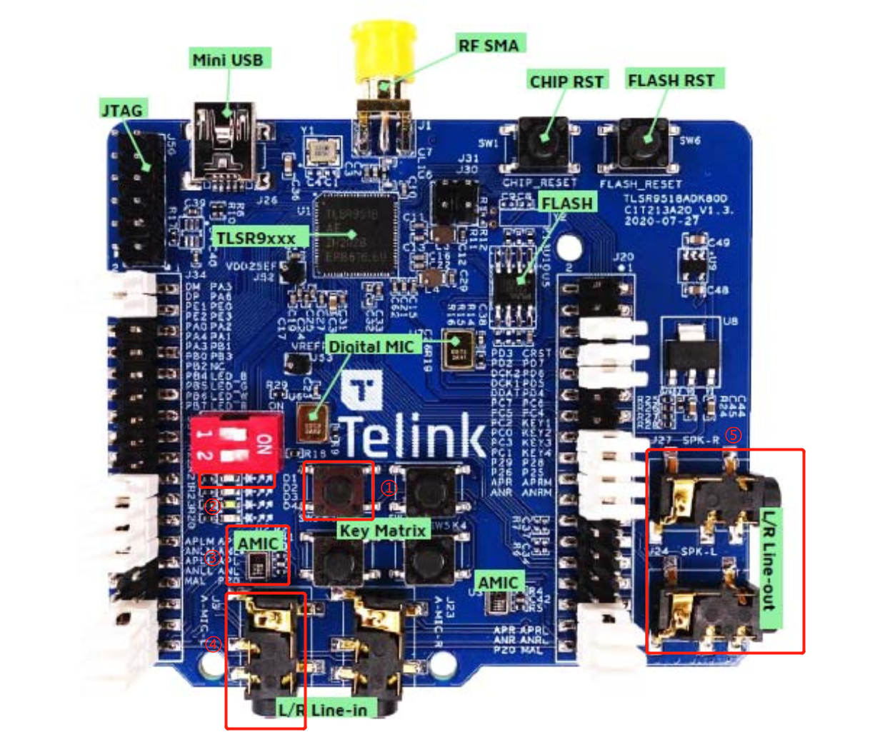
EVB Development Board
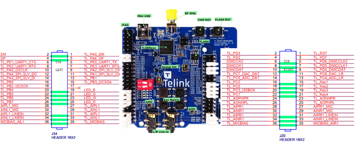
For details of EVB development board, please refer to "Telink TLSR9518A Generic Starter Kit Hardware Guide_internal_V1.0.pdf" document.
Line-in Input
There are left and right linein inputs, which can be single-ended or differential, and EVB defaults to differential connection.
Single left linein:
Short circuit
AIPL1_LINEIN(J34_32)--TL_AIPL1(J34_31)
AINL1_LINEIN(J34_34)--TL_AINL1(J34_33)
Turn off
AIPL1_MIC(J34_28)--TL_AIPL1(J34_27)
AINL1_MIC(J34_30)--TL_AINL1(J34_29)
MICBIAS_AIL1(J34_36)--TL_MICBIAS(J34_35)
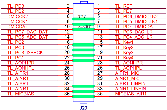
Single right linein:
Short circuit
AIPR1_LINEIN(J20_32)--TL_AIPR1(J20_31)
AIPR1_LINEIN(J20_34)--TL_AINL1(J20_33)
Turn off
AIPR1_MIC(J20_28)--TL_AIPR1(J20_27)
AINR1_MIC(J20_30)--TL_AINR1(J20_29)
MICBIAS_AIR1(J20_36)--TL_MICBIAS(J20_35)
AMIC Input
There are left and right AMIC inputs, which can be single-ended or differential, and EVB defaults to differential connection.
Single left AMIC:
Short circuit
AIPL1_MIC(J34_28)--TL_AIPL1(J34_27)
AINL1_MIC(J34_30)--TL_AINL1(J34_29)
MICBIAS_AIL1(J34_36)--TL_MICBIAS(J34_35)
Turn off
AIPL1_LINEIN(J34_32)--TL_AIPL1(J34_31)
AINL1_LINEIN(J34_34)--TL_AINL1(J34_33)
Single right AMIC:
Short circuit
AIPR1_MIC(J20_28)--TL_AIPR1(J20_27)
AINR1_MIC(J20_30)--TL_AINR1(J20_29)
MICBIAS_AIR1(J20_36)--TL_MICBIAS(J20_35)
Turn off
AIPR1_LINEIN(J20_32)--TL_AIPR1(J20_31)
AIPR1_LINEIN(J20_34)--TL_AINL1(J20_33)
DMIC Input
The DMIC requires only two signal traces: data and clk, with a fixed clock frequency of 3MHz for clk.
Dual-DMIC configuration requires a single data trace, which is shared between both DMICs, and two clk traces, which are synchronized. The primary DMIC captures data on the rising edge of the clk signal, and the secondary DMIC samples on the falling edge.
Short circuit
Common data shared by left and right Mic: DMICDAT (J20-10) -- TL_PD4_DMICDAT (J20-9)
Left Mic: DMICCK1(J20-8)--TL_PD6_DMICCLK1(J20-7)
Right Mic: DMICCK2(J20-6)--TL_PD6_DMICCLK2(J20-5)
USB Port
Short circuit
DM(J34-2)--TL_PA5_DM (J34-1)
DP(J34-4)--TL_PA6_DP (J34-3)
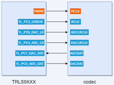
I2S Port
Support I2S master-slave mode, but it is recommended that TRLS9XXX I2S be the Master, and being the master does not require asynchronous resampling to reduce computational load.
Running Example
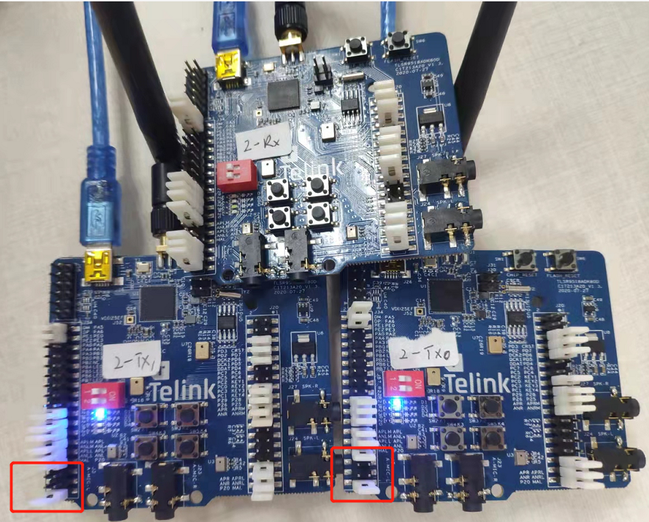
Hardware Preparation
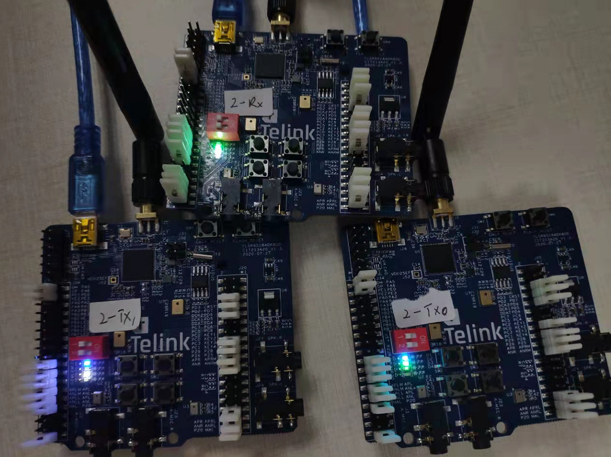
Three EVB boards and three USB cables are required.
Instructions:
Pairing button: short press to enter pairing status, double press to exit pairing status.
Connection status indicator: fast blinking for pairing status, slow blinking for reconnection status, and always on for connection status.
As shown above, the L Linein input and Lineout output are used, if an AMIC is used as input, the Tx side J34 needs to be short circuited as shown in the red box below.
Software Burning
Two EVBs as TX to burn img_proj_live_mic_tx.bin and one EVB as RX to burn img_proj_live_mic_rx.bin (firmware is in release_bin directory), the steps are as follows:
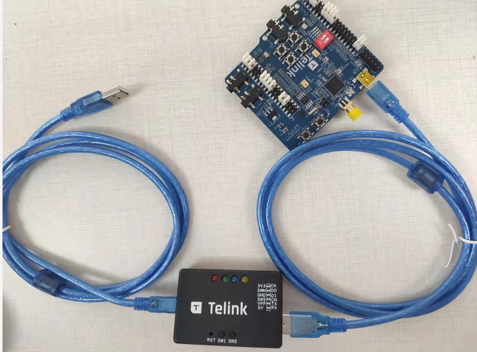
Step 1: Prepare the Telink burner and connect it as shown in the figure below.
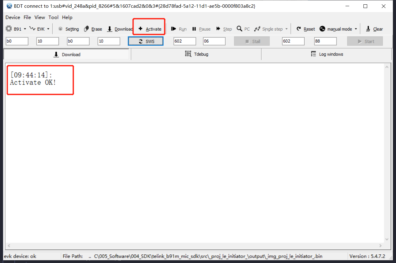
Step 2: Open the Telink BDT.exe program.
Step 3: Click Activate.
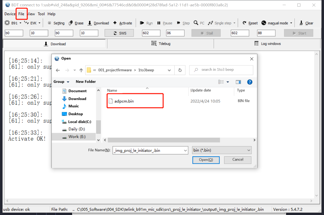
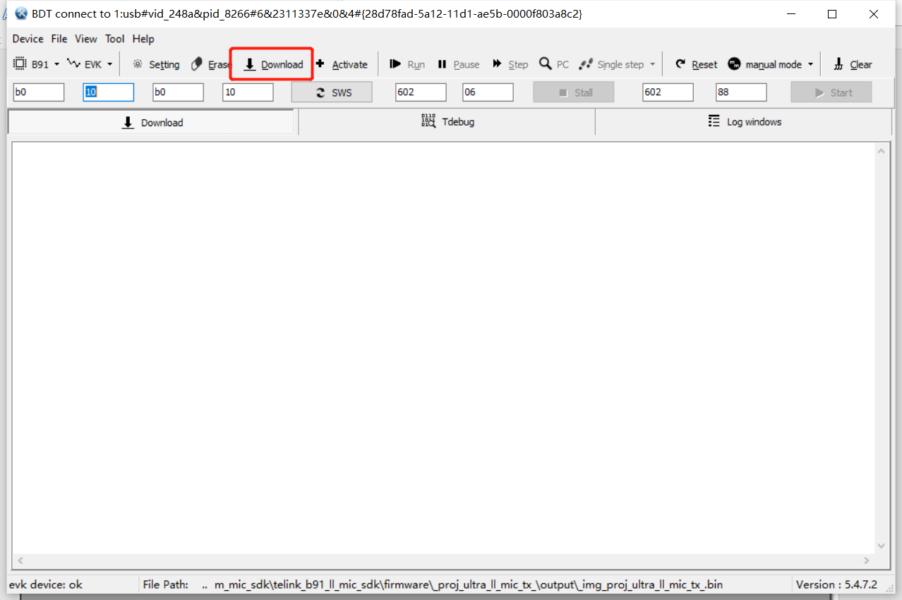
Step 4: Click File and in the drop down list click Open.
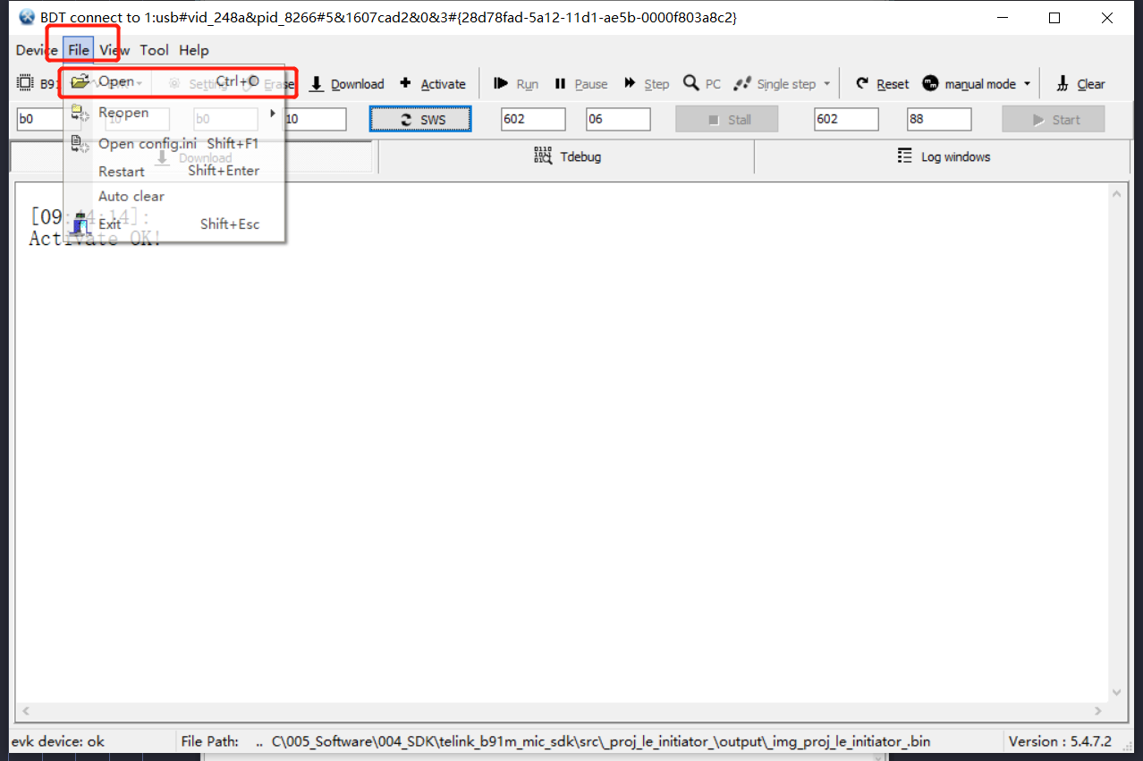
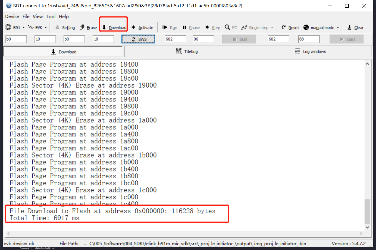
Select the firmware to be burned and click Download as shown below:
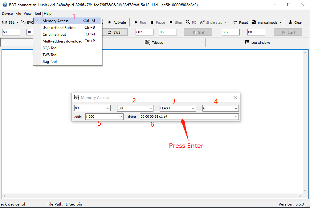
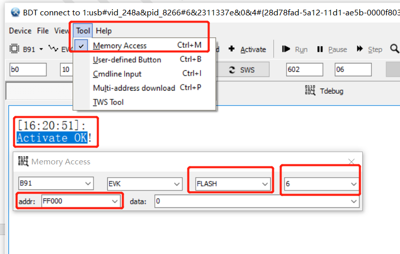
Step 5: Burn MAC address, open Memory Access, operate and fill in the MAC address as the numerical order in the following figure. To burn the MAC address as: 0xa4c138000000, fill in: 00 00 00 38 c1 a4, as shown below, after filling in, press Enter to burn. (For more operations of BDT tool, visit: http://wiki.telink-semi.cn/wiki/IDE-and-Tools/Burning-and-Debugging-Tools-for-all-Series/)
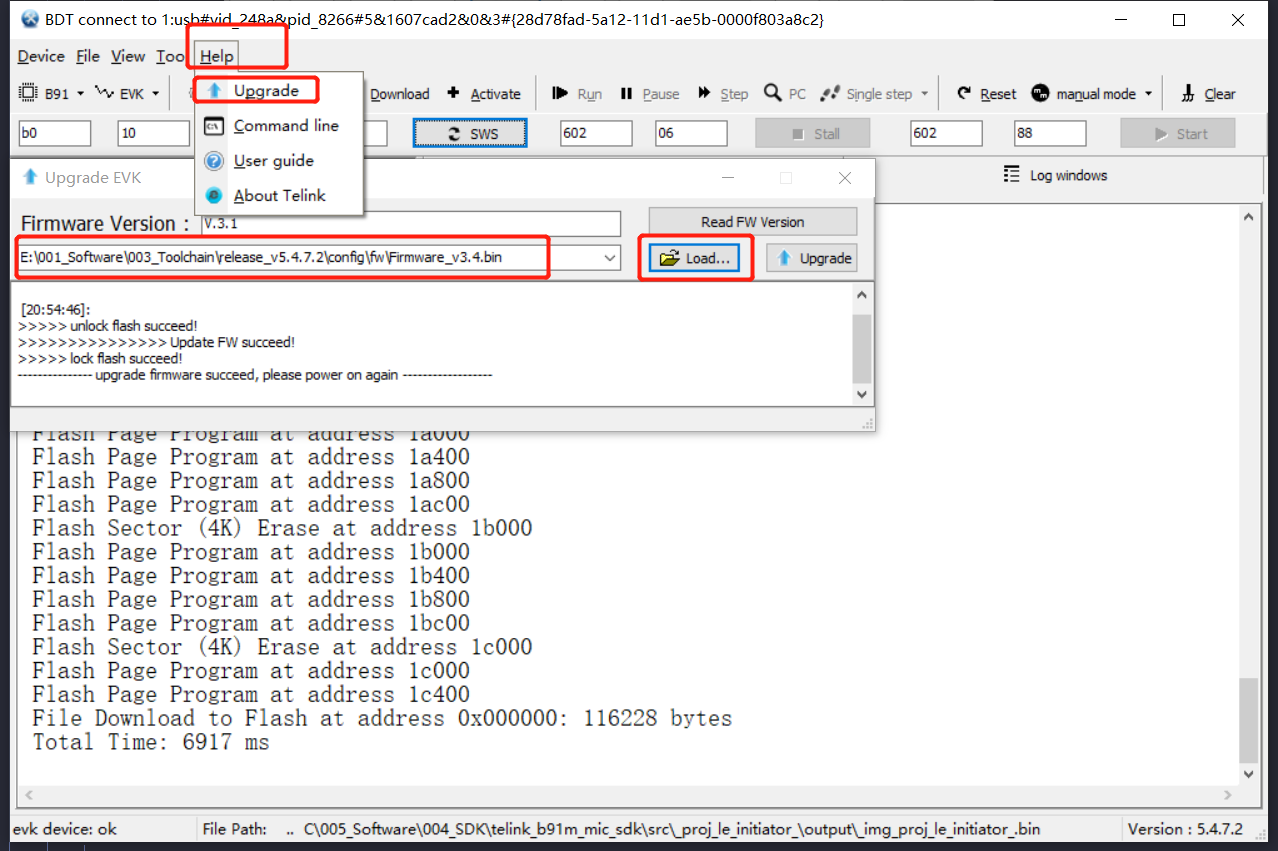
Note that when the burner fails to activate, it is needed to upgrade the firmware of the burner, as shown in the following figure, click Help, select Upgrade, load the firmware under the path of the burner software, and finally reseat the burner.
Running
After re-powering, short press the SW2 button on TX0 and RX respectively to pair TX0, and then press the SW2 button on TX1 and RX respectively to pair TX2. After successful pairing, the blue lights of TX0 and TX1 are always on, at the same time, the green and white lights indicating the channel will be on respectively while the green and white lights of Rx will light up at the same time, as shown in the figure:
Finally, audio can be monitored through the Lineout interface.
Note
- Lineout on the Tx side outputs the audio encoded and then decoded from the local AMIC pickup, while Lineout on the Rx side outputs the audio decoded from the encoded audio data sent from the far end, Tx0 and Tx1, respectively.
- Where Tx0 with a green light is the left channel and Tx1 with a white light is the right channel.
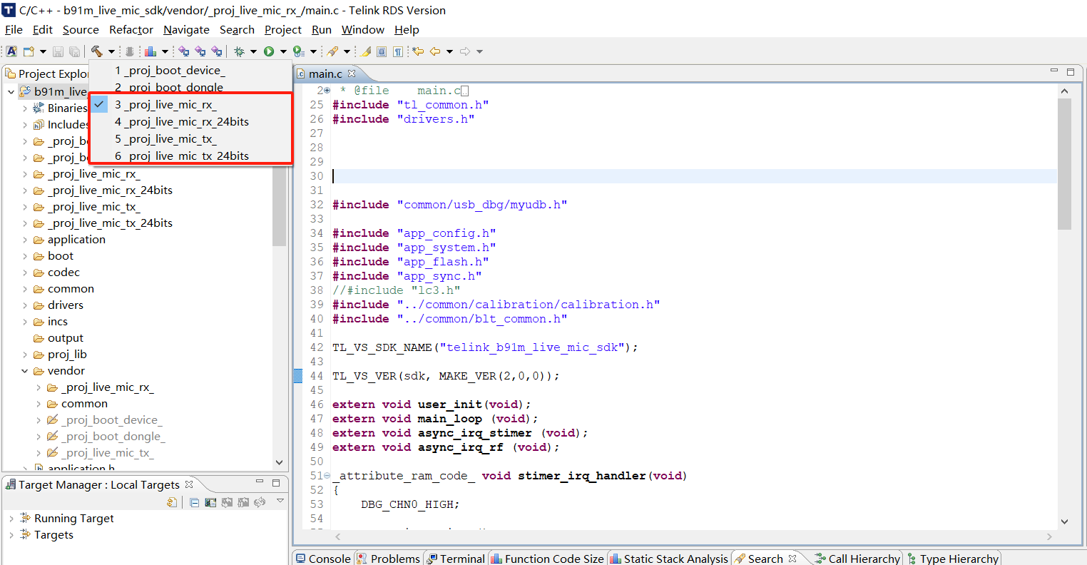
SDK Compiling
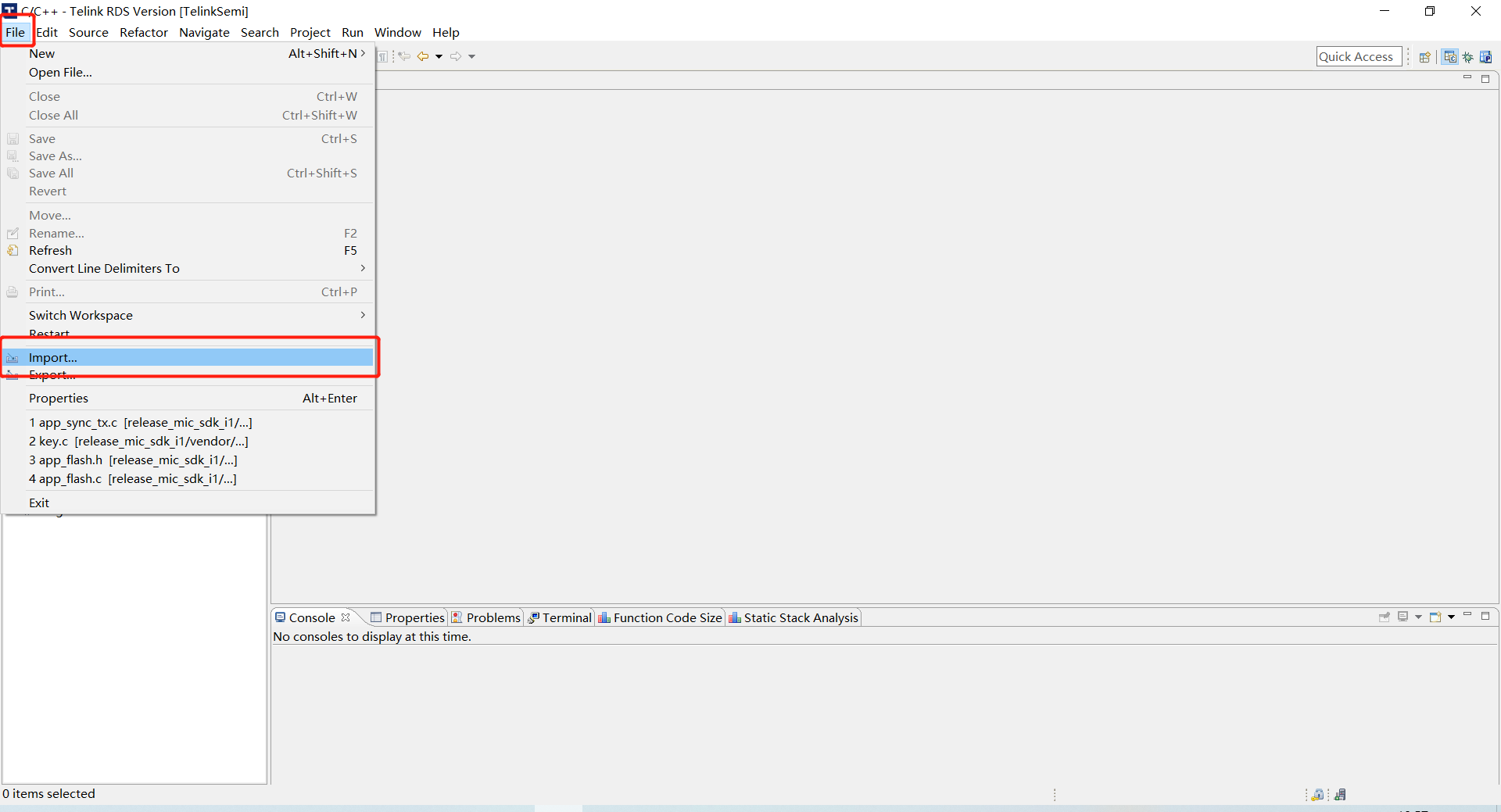
Import
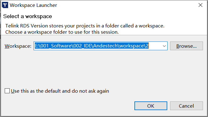
When opening AndeSight IDE for the first time, a dialog box for selecting a workspace will pop up, browse to select a directory as the workspace. Any directory can be selected as the workspace directory.
Select File -> Import, as shown below:
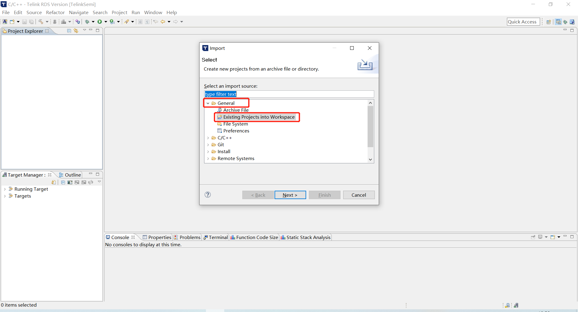
In the pop-up window, click General and select Existing Projects into Workspace.
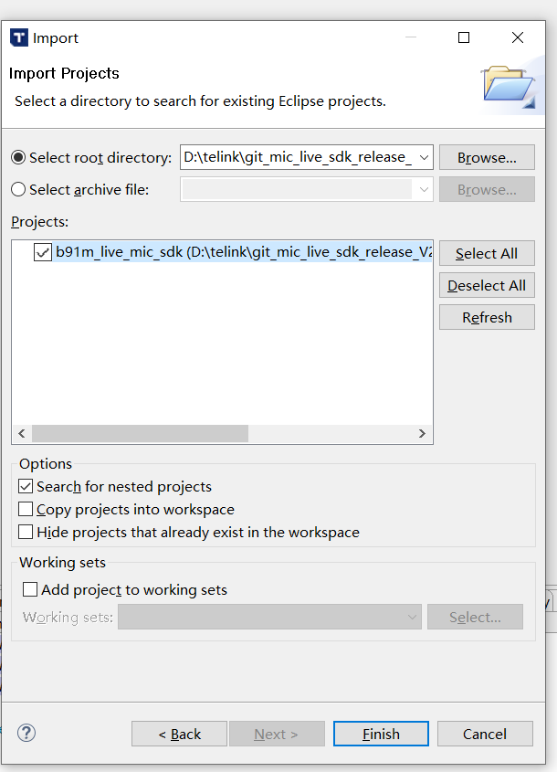
In the Select root directory box, enter the path where the SDK is located, or directly click Browse and select the directory where the SDK is located, then check the SDK, click Finish, then projects can be imported (Note: It is recommended that the IDE working path and the path where the SDK source code is located be different, so that it is easy to open multiple projects).
Compiling
The bin to be burned after compilation is the merged firmware (with img* header), including:
(1) Boot project with bootloader: used for program jump as well as ota.(proj_boot*)
(2) App project: the actual running software. (proj_live_mic*)
The IDE script will merge the above two projects into the firmware with img header automatically and save it to the app project generation directory like:
b91m_live_mic_sdk\proj_live_mic_tx\output\img_proj_live_mic_tx.bin
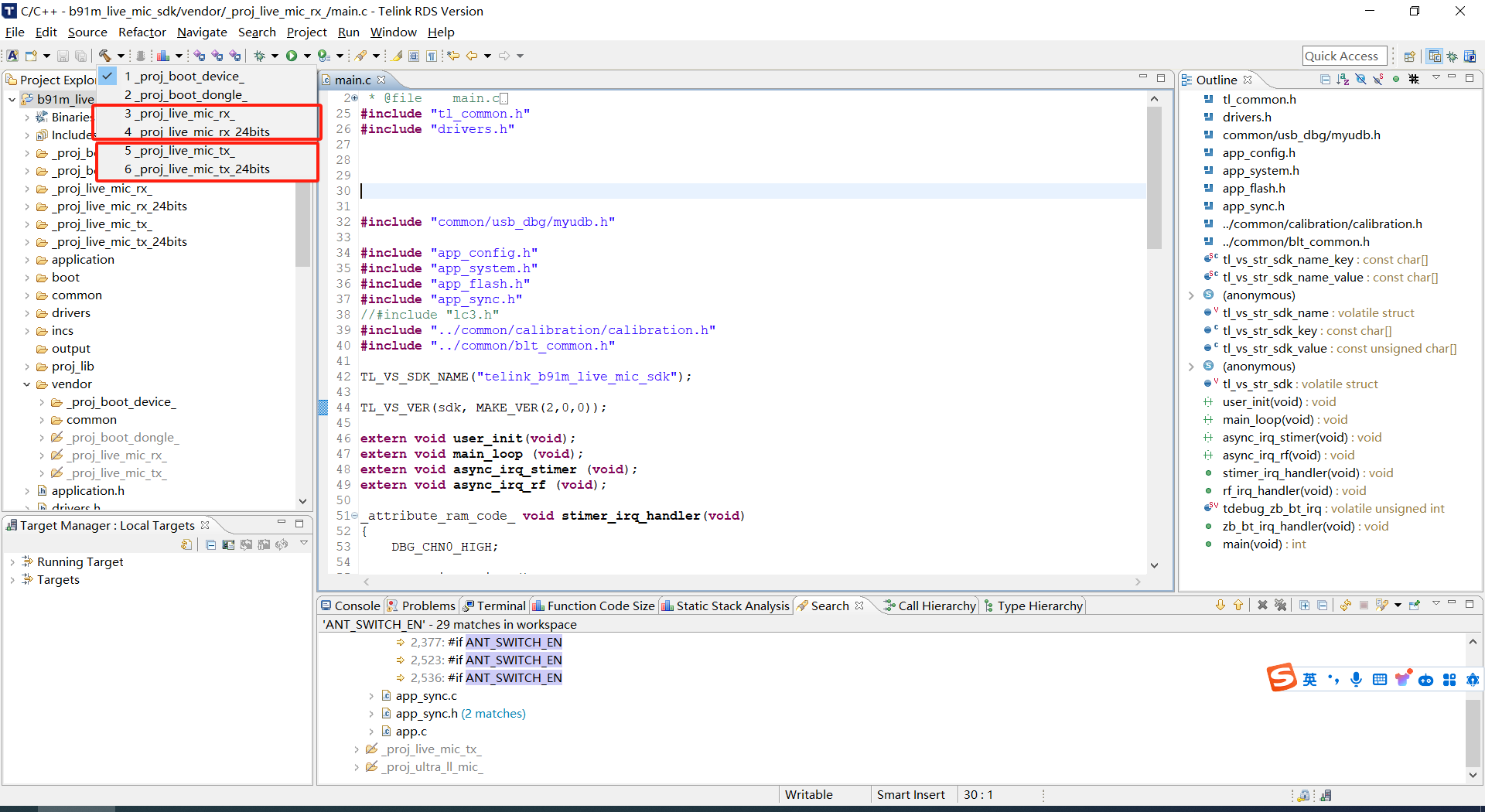
Therefore, when compiling the app project for the first time, it is needed to compile the proj_boot_device and proj_boot_dongle projects first, which will be used to generate the merged firmware later.
Note
- When compiling for the first time, it is needed to compile the two boot projects before compiling the whole project, otherwise there will be an error.
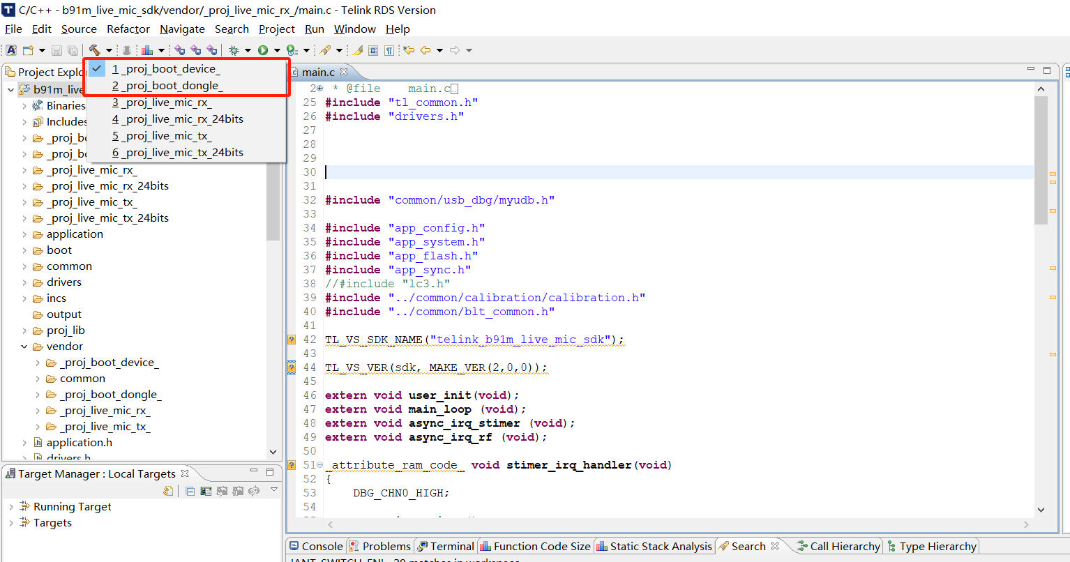
Then compile 3 (RX side 16bit) and 4 (RX side 24bit) or 5 (TX side 16bit) and 6 (TX side 24bit) projects.
Common Tools
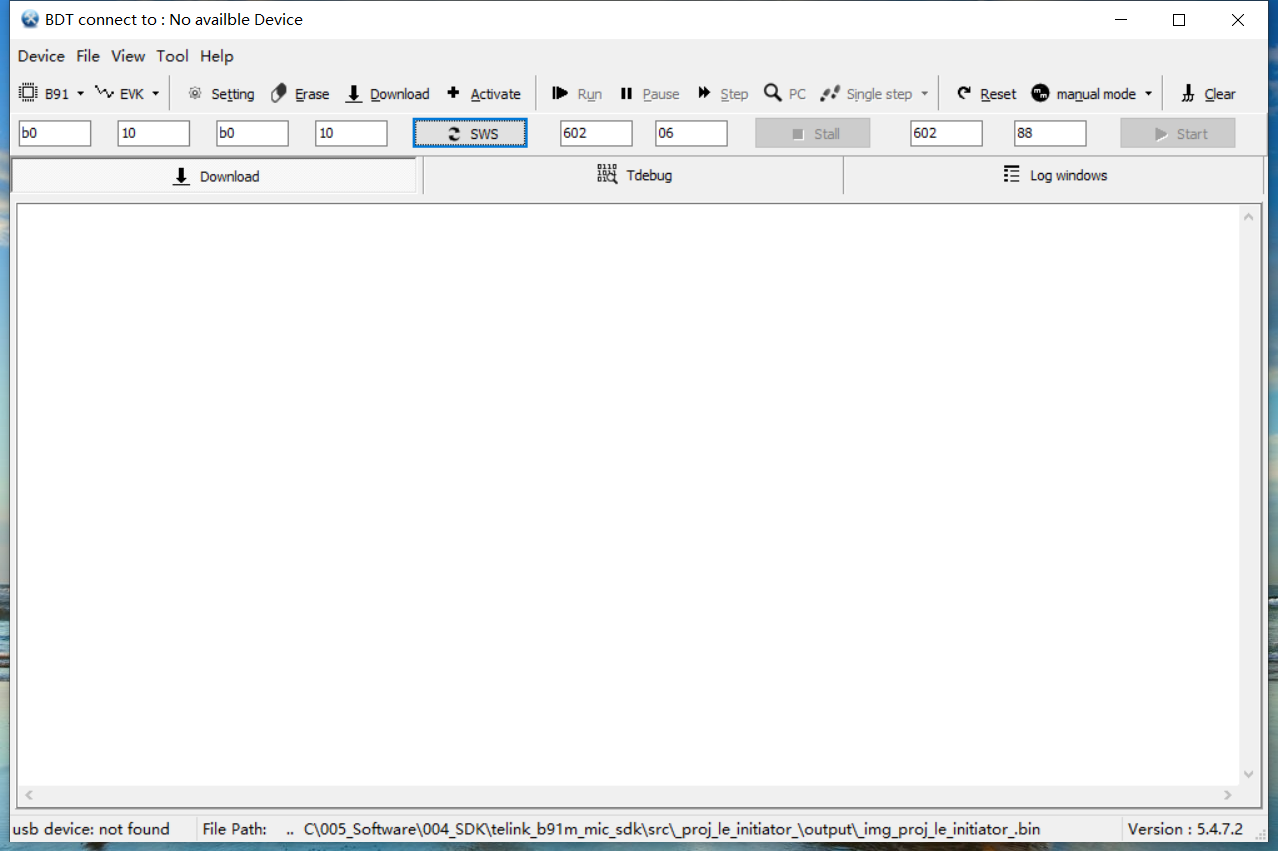
Telink BDT
Telink BDT tool's full name is Telink Burning and Debugging Tool and refer to the Tool User Guide document for its specific functions, listed below are a few common application scenarios.
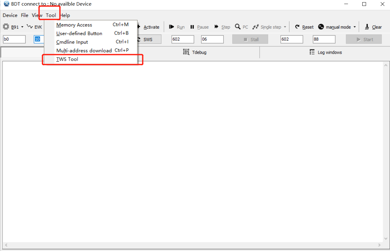
Multi-bin File Download Tool
Telink BDT is based on TWS and realizes the function of burning multiple bin files, which is also applicable to this SDK. The usage is as follows:
Step 1: Click Tool and select TWS Tool from the drop down menu.
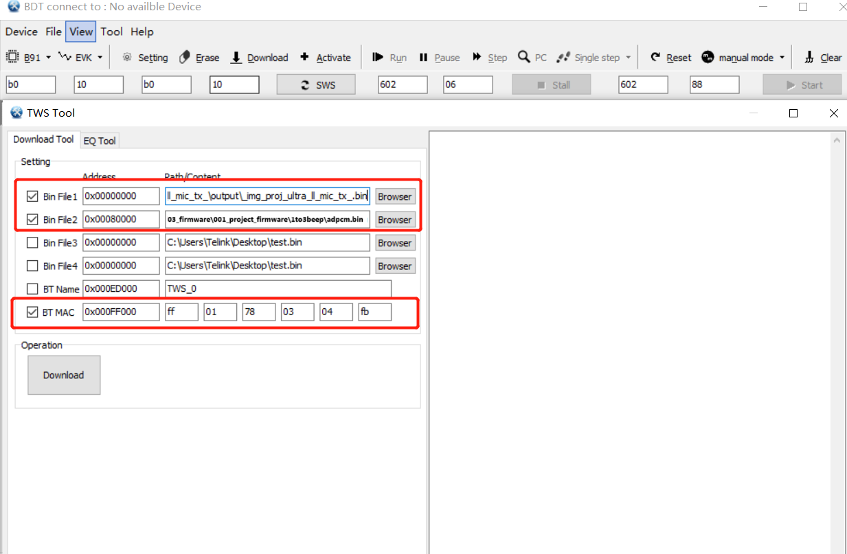
Step 2: Select Download Tool page, check Bin File1, Bin File2 and BT MAC respectively, and select the corresponding program firmware, beep file and fill in the MAC address, click Download to burn the program, beep and MAC address at the same time.
Independent Beep Burning
For the beep function the SDK supports by default, it is needed to burn the beep file at the specified address, the specific steps are shown below:
Step 1: Open Telink BDT, click Setting and enter 0x80000 at Download Addr in the pop-up window.
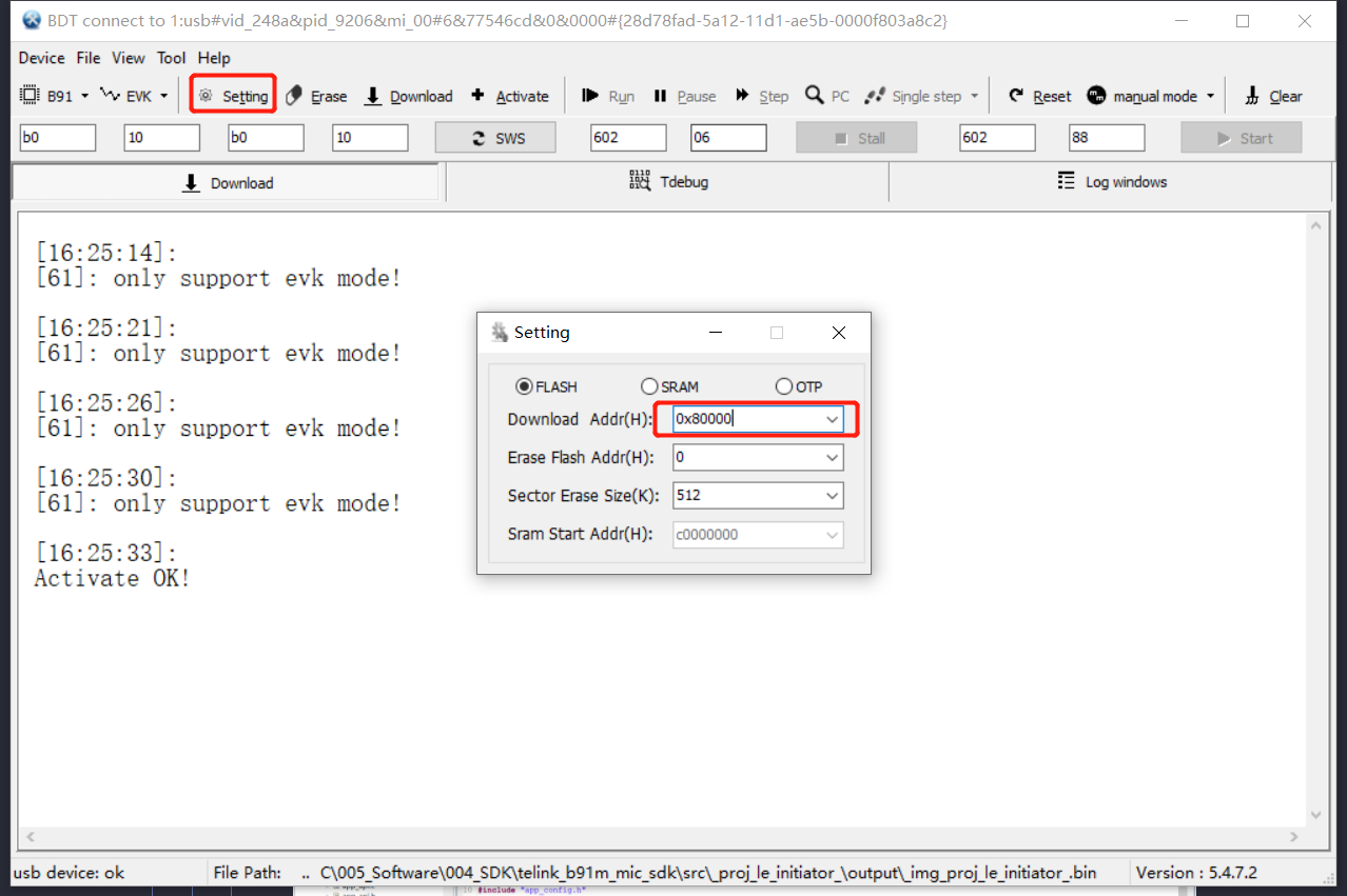
Step 2: Select the 48k ADPCM beep file.
Step 3: Click Download to burn the beep.
MAC Address Independent Read/Write
Interference may occur when the Mac addresses are the same on both Tx sides, so the Mac address can be read and written via the Telink BDT.
Step 1: Open Telink BDT, click Activate, in the case of Activate OK, click Tool, select Memory Access, in the pop-up window select Flash for Memory Type, enter 6 for size, and FF000 for addr.
Then press tab to read the MAC address stored at that address: e0 33 8e 8b 70 2b.
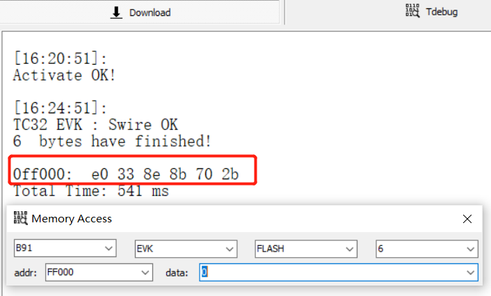
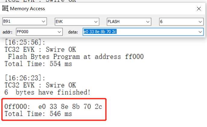
Step 2: Enter the Mac address to be modified in the DATA section: e.g. e0 33 8e 8b 70 2c and press enter to write it.
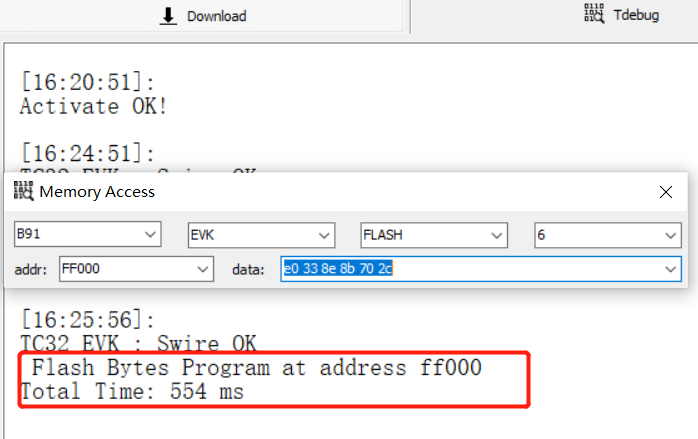
Press tab again to read the data at that address and ensure that the write was successful.
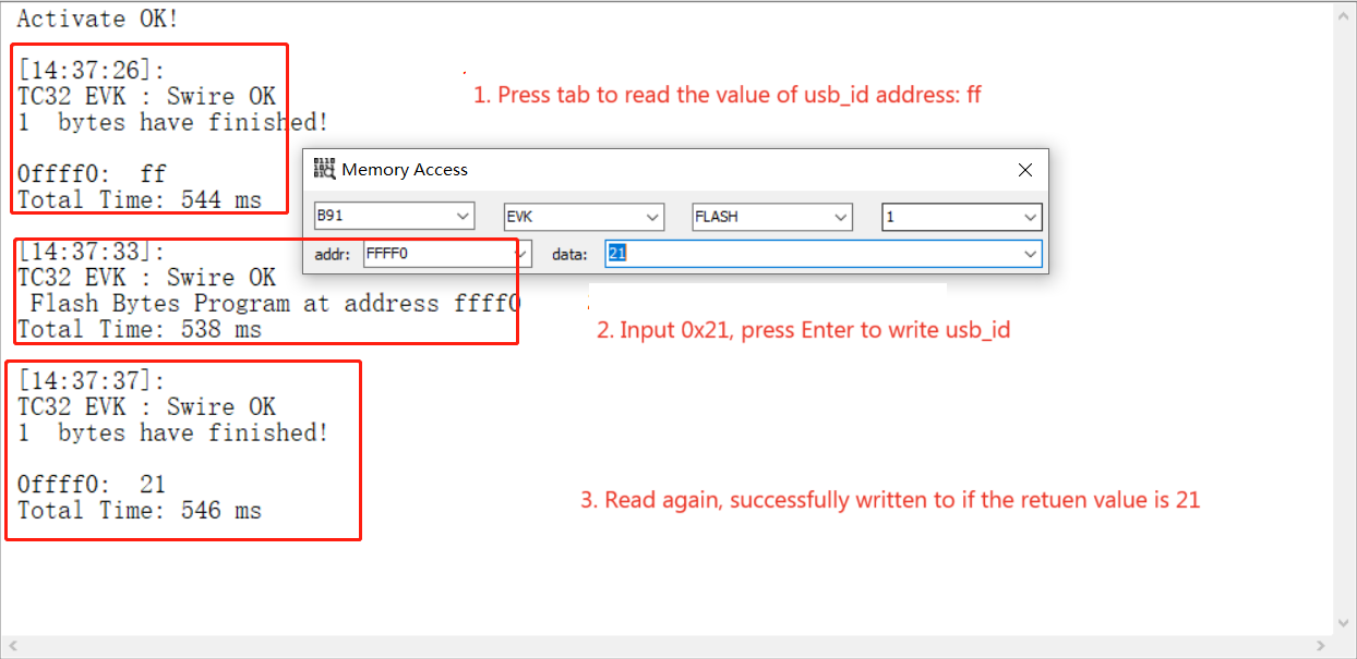
Burn Specified USB_ID to the TX Side
In 2-to-1 mode, the default starting address of the TX side is 0x120 (determined by the 0xFFFF0 address where Flash_SYS_USER_USBID_ADDR is located).
void user_init(void)
{
    ......
#if (APP_BUILD == APP_MIC_TX)
    uint16_t usb_id = 0x120;
    uint8_t flag = 0;
    app_Flash_read(Flash_SYS_USER_USBID_ADDR, sizeof(flag), (u8 *)&flag); //Flash_SYS_USER_USBID_ADD - 0x7FFF0
    if (flag != 0xFF) {
        usb_id = 0x100 + flag;
    }
    ......
}
To view logs of multiple TXs, it is needed to modify the addresses where the usb_id of the different TX sides are located to differentiate them, so as to be consistent with the pid configuration of the risc_v_tdb tool.
Then just synchronize the corresponding values in the pid configuration of the risc_v_tdb tool.
risc_v_tdb
USB Print and View
USB printing log can use the following function, whose parameter 'str' is for the string to be printed, 'ph' for the data to be printed, 'n' for the length of bytes. Set unnecessary parameters to 0 if you only need to print strings or data.
void usb_send_str_data (char *str, u8 *ph, int n);
The function has the following common wrappers:
void usb_send_str_data (char *str, u8 *ph, int n)
int usb_send_str_int (char *str,int w);
void usb_send_str_u32s (char *str, u32 d0, u32 d1, u32 d2, u32 d3);
#define my_dump_str_data(en,s,p,n)
#define my_dump_str_u32s(en,s,d0,d1,d2,d3)
Developers can call based on needs.
To support USB printing, configure APP_MODE to APP_MODE_DEBUG_ONLY or APP_MODE_DEBUG_HID in the app_config.h file first.(using the risc_v_tdb tool to view the log in APP_MODE_AUDIO_AUTO mode is not available, use the USB to serial port tool instead)
......
/////   4 different mode //////////

#if (APP_BUILD == APP_MIC_RX)
    #define     APP_MODE               APP_MODE_DEBUG_ONLY    //APP_MODE_AUDIO_AUTO
#else
    #define     APP_MODE               APP_MODE_DEBUG_ONLY    // APP_MODE_DEBUG_ONLY or APP_MODE_DEBUG_HID
#endif

//////////////////////////// APP Mode: setting //////////////////////////////
......
Then open different configurations based on different pids, where the default pid on the Tx side is 0x1209218, and the default pid on the Rx side is 0x1239218, which consists of usb_id and pid.
(1) Tx side usb_id
void user_init(void)
{
    ......
#if (APP_BUILD == APP_MIC_TX)
    uint16_t usb_id = 0x120;
    uint8_t flag = 0;
    app_Flash_read(Flash_SYS_USER_USBID_ADDR, sizeof(flag), (u8 *)&flag); //Flash_SYS_USER_USBID_ADD - 0x7FFF0
    if (flag != 0xFF) {
        usb_id = 0x100 + flag;
    }
    ......
}
Since Tx is divided into Tx0 and Tx1 in 2-to-1 mode, a usb_id definition is possible.
(2) Rx side usb_id
void user_init(void)
{
    ......
#elif(APP_BUILD ==APP_MIC_RX)
    uint16_t usb_id = 0x123;
#endif
    ......
}
Define the full pid in the app_usb_desc.c file.
#if (APP_MODE & FLAG_PRINTER_DEBUG)
    const USB_Descriptor_Device_t my_device_desc_audio  = MYDESC_DEVICE(0x0110, 0x248a, 0x9218);
Next create different configurations based on different pids: Tx0, Tx1, and Rx.
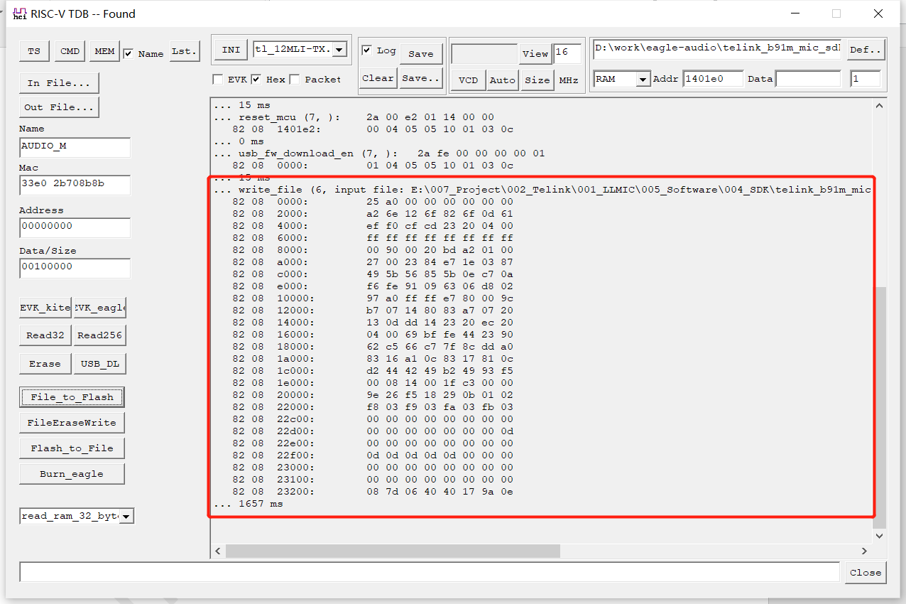
Flash Read/Write
(1) risc_v_tdb supports the function of writing to flash online, thus realizing the demand of directly upgrading the program online during the debugging process:
Step 1: Select the corresponding configuration, and after successful connection, click In File to select the firmware to be upgraded.(Note: Before writing to the firmware, the MAC address can be synchronized by modifying the MAC option box)
Step 2: Click File_to_Flash to write to the firmware.
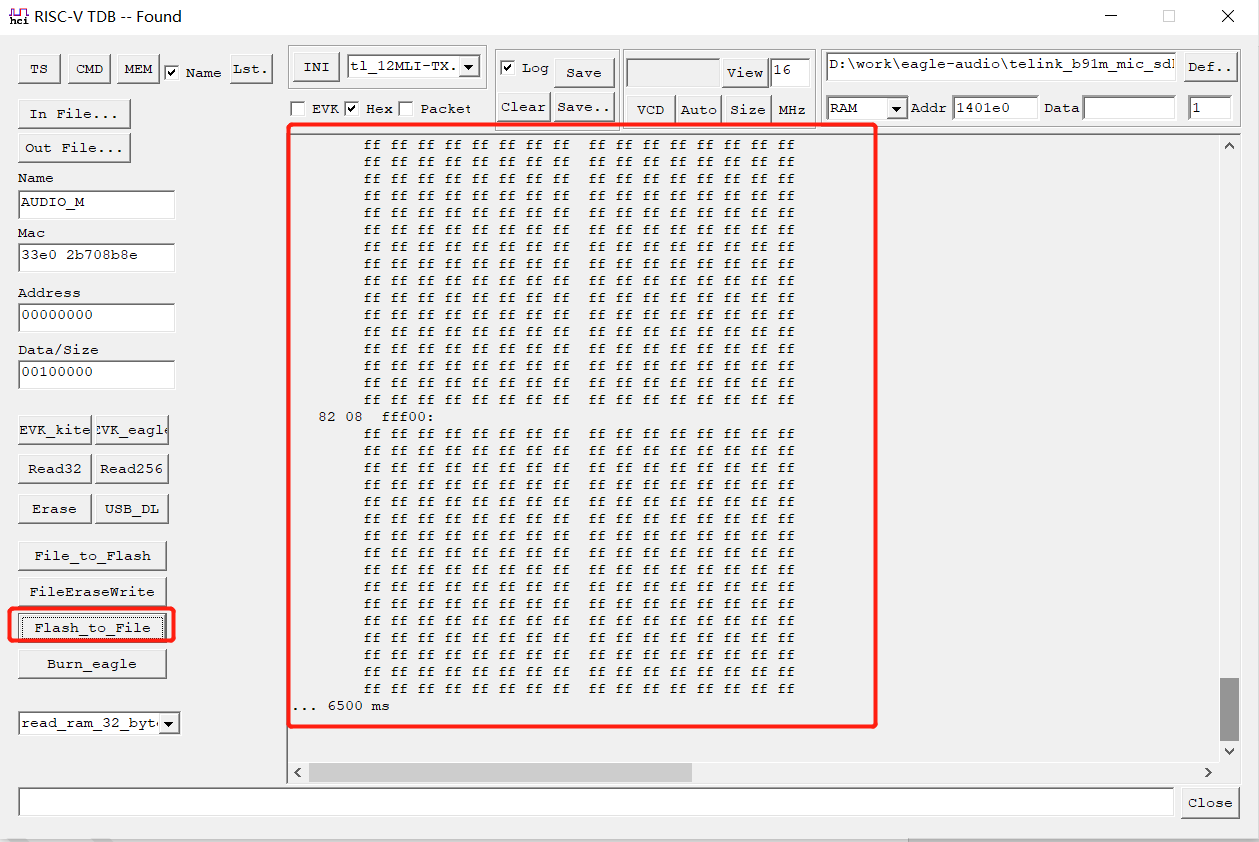
(2) In addition to this, risc_v_tdb supports reading flash and saving it as a file:
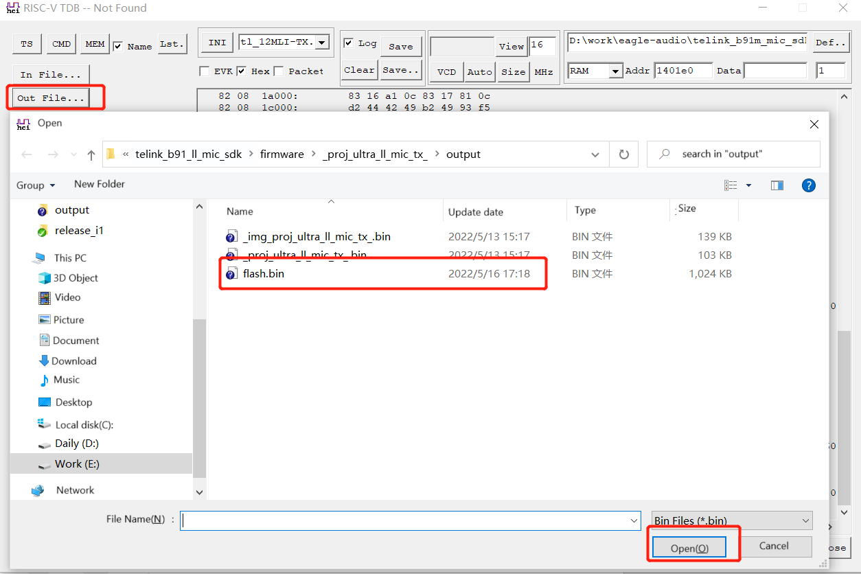
Step 1: Select a configuration that supports reading flash and saving it as a file.
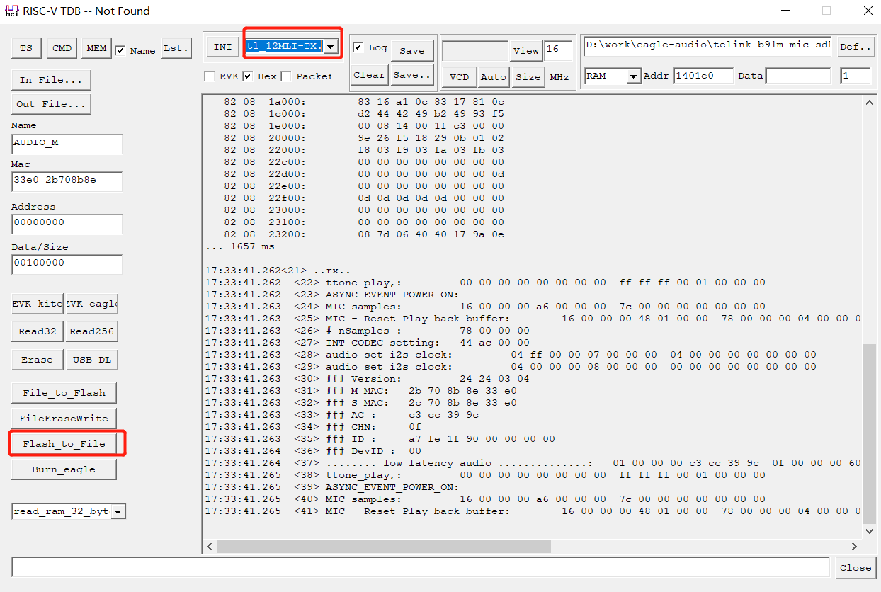
Step 2: Click Out File to select the bin file to be written to flash.
Step 3: Enter the start address of the flash to be read and the read length.
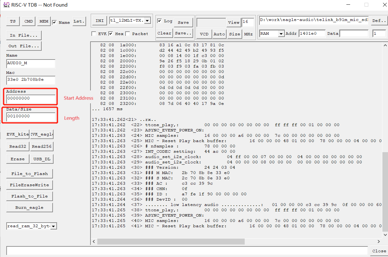
Step 4: Click Flash_to_File to save the read flash to a bin file.
Send Command
risc_v_tdb supports the function of sending commands to control the program: based on the USB Print mode, users can add the control function of the project in the my_usb_audio_debug interface, and the functions supported at present are: pairing test control, EMI test control, beep test control, data transmission test control, and noise reduction function test control.
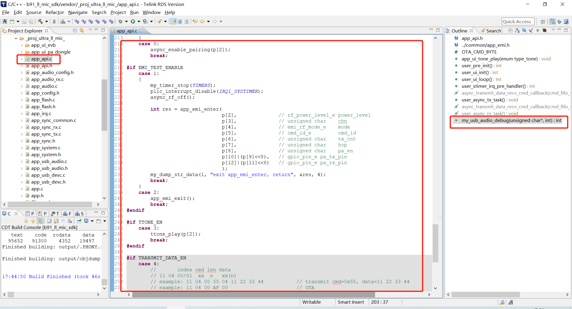
The specific control method is as follows:
Step 1: connect risc_v_tdb to the board and open the function to configure the corresponding macros: EMI_TEST_ENABLE, TTONE_EN, TRANSMIT_DATA_EN, APP_NS_ENABLE and so on.
Step 2: Enter the corresponding command in the command box, such as 11 00 20, and type Enter.
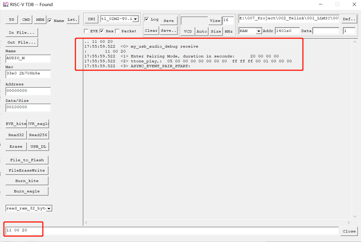
Where 11 is the command header, 00 is the value corresponding to the pairing test control, and 20 is the pairing test incoming parameter. Other test controls are as above.
VCD Waveform
VCD Basic Knowledge
Value Change Dump (VCD), an ASCII-based format for dump files generated by EDA logic simulation tools. In 1996, IEEE Std. 1364-1995, along with the Verilog hardware description language, defined the standard four-value VCD format. Six years later, the extended VCD format defined in IEEE Std. 1364-2001 supports the recording of signal strength and directionality. The simple and compact structure of the VCD format has made its use ubiquitous and extends it to non-Verilog tools, such as the VHDL simulator GHDL and various kernel tracers. One limitation of the format is that it cannot record values in memory.
The contents of the VCD file are divided into a title section, a variable definition section, a variable initialization section, and a value change section. The title section contains timestamp, simulator version number, and timescale, which maps the time increments listed in the value change section to simulated time units. The variable definition section contains scope information and a list of signals instantiated within a given scope. The initialization section contains the initial values of all dumped variables. The value change section contains a series of chronological value changes for the signals in a given simulation model.
VCD files are required in order to record value changes.
VCD Function Description
(1) Print event, this function will invert the value of the variable twice, and form a pulse. The function ID must be an event type variable, and the function will only output information about the value change, not the time information, and its value change will be followed by the most recent timestamp.
log_event(en,id)
e.g. log_event(1, SLET_timestamp)  //Will invert the value of SLEV_reserved twice, 0->1,1->0.
(2) Print event and time, this function will invert the value of the variable twice, and forms a pulse. The function ID must be a variable of type event with tick, and the function will output information about the value change and the time.
log_tick(en,id)
e.g. log_tick(1, SLET_timestamp)
(3) Print data, the following three functions are for printing 1/8/16bit data, en is enable, id is the variable name (the semaphore in the previous subsection, it is needed to use the variable name of 1/8/16bit data type), and b is the changed value. It will write the value change of the variable and the current time to the VCD file.
log_task(en,id,b) //print 1bit data
e.g. log_task(1, SL01_TX_EN,1)   //Change the value of SLET_timestamp to 1 at the current time point
log_task(1, SL01_TX_EN,0)   //Change the value of SLET_timestamp to 0 at the current time point

log_b8(en,id,d)   //print 8bit data
e.g. log_b8 (1, SL08_lmp_rx_code,1)
log_b16(en,id,d)  //print 16bit data
e.g. log_b16 (1, SL16_bt_CLKN_HS,1)
risc_v_tdb Generates VCD File to View Time Series
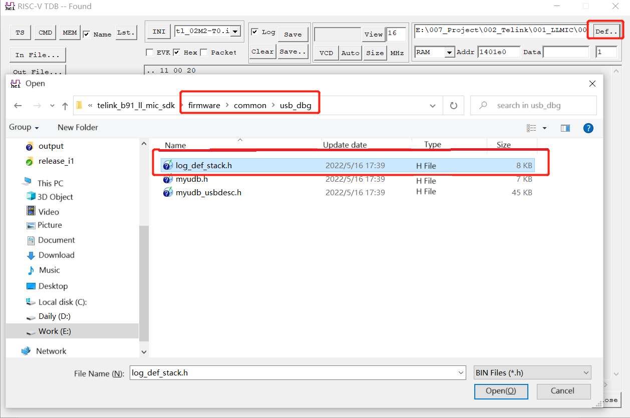
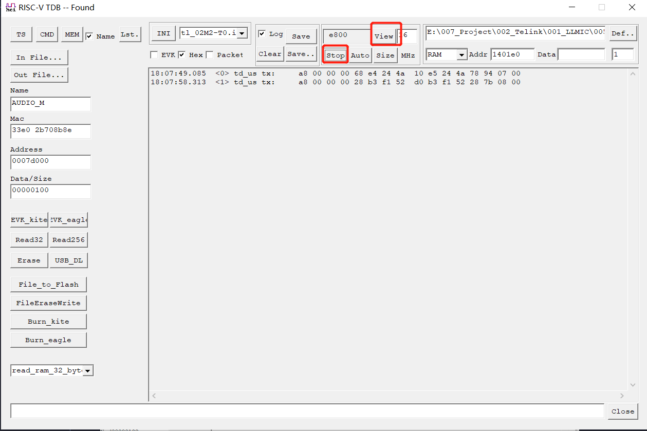
When APP_MODE is configured as APP_MODE_DEBUG_ONLY or APP_MODE_DEBUG_HID, risc_v_tdb supports the vcd waveforms viewing function of Telink's own protocol based on usb print, and it can view the execution status of each function, and the specific viewing steps are as follows:
Step 1: In the connected case, click Def and select the log_def_stack.h file under the path common\usb_dbg.
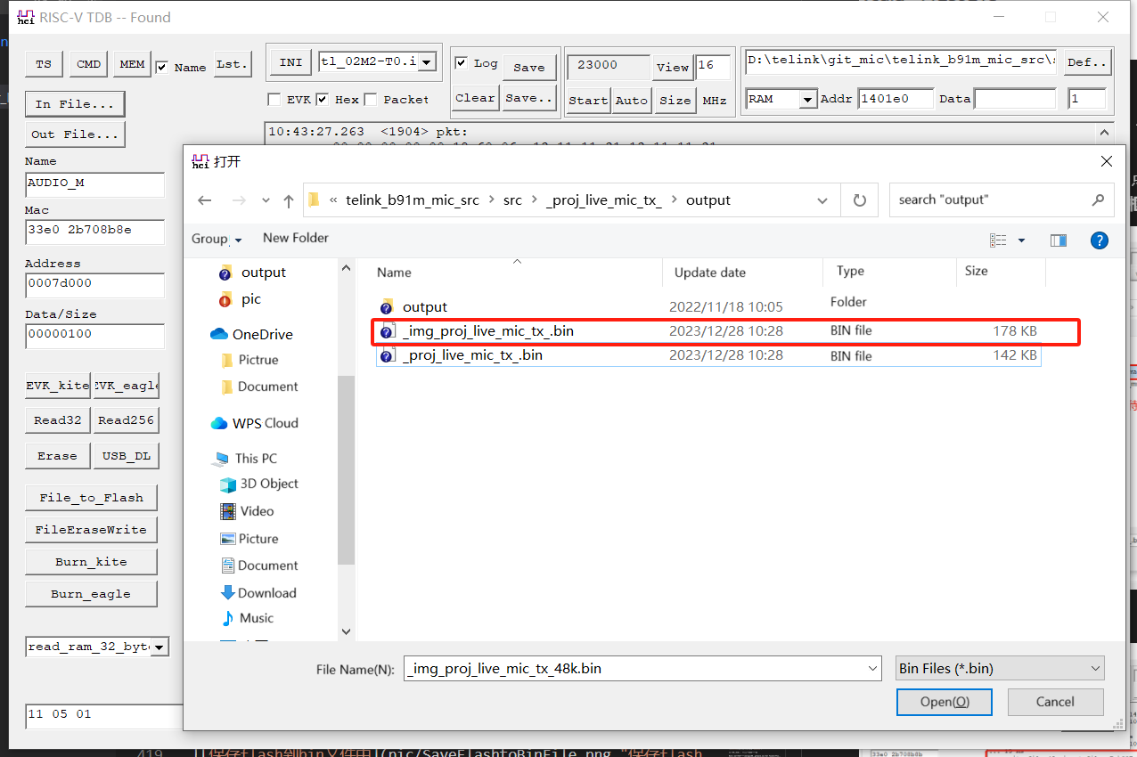
Step 2: Click In File and select the firmware generated under firmware\proj_live_mic_tx\output path (take proj_live_mic_tx as an example here).
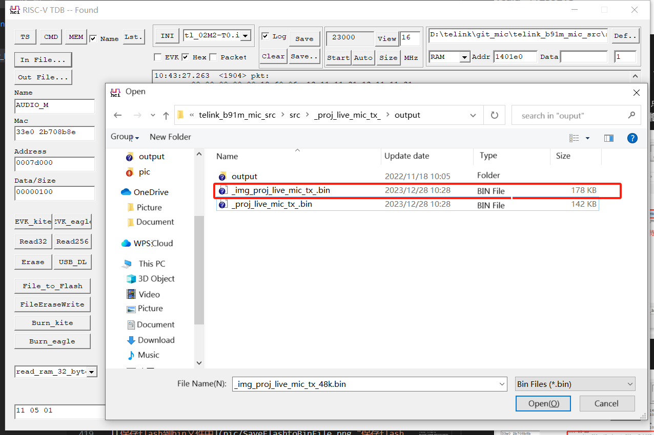
Step 3: Click on the VCD to capture:
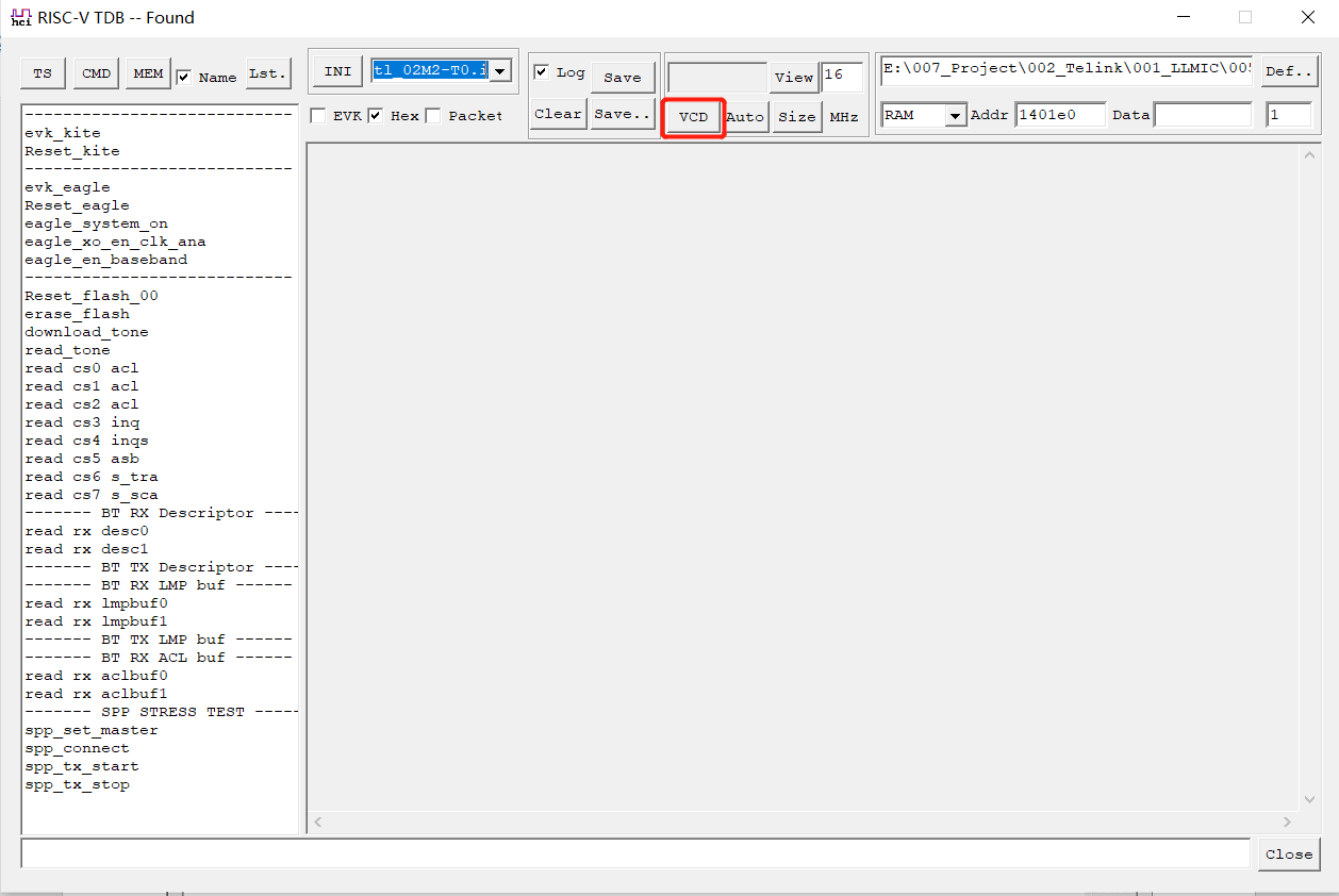
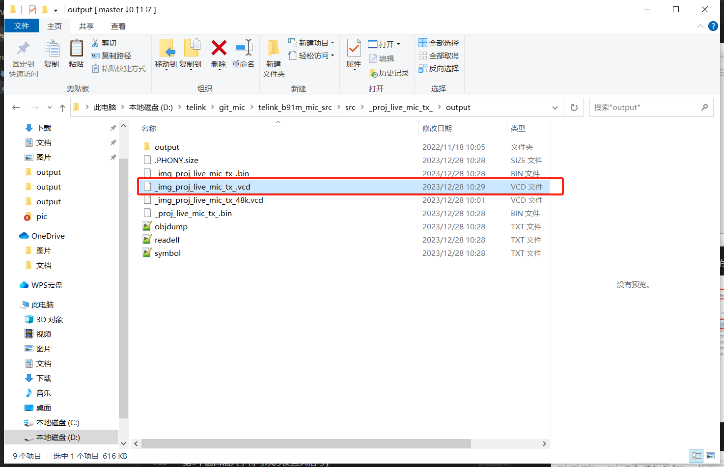
Click Stop after a certain amount has been collected, and the vcd file will be automatically saved to the corresponding output folder of the project.
Then click View and jump to the Waveform Viewing tool.
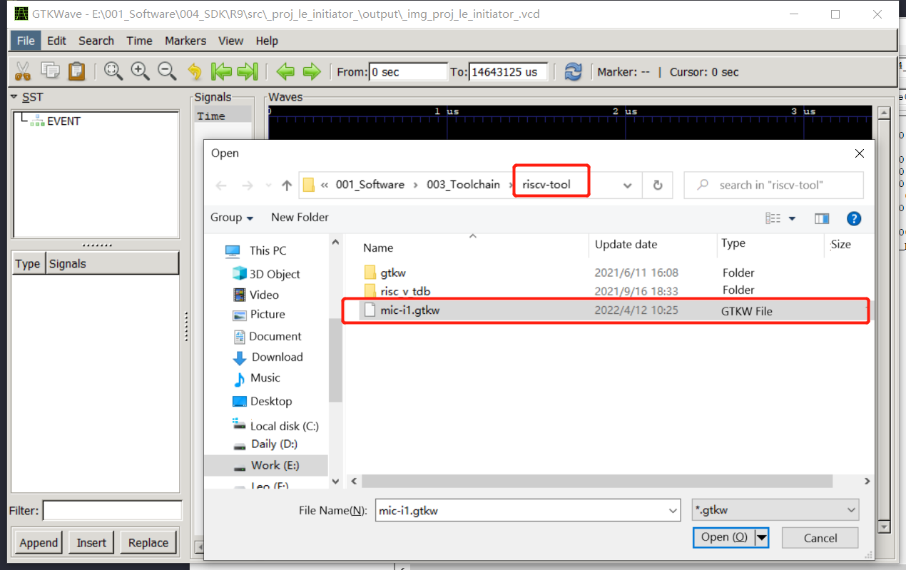
Step 4: In the tool that pops up, click File and select Read Save File.
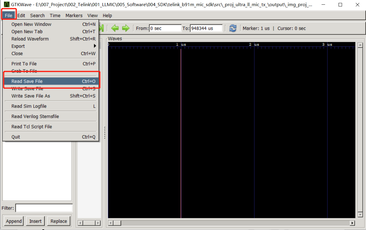
Select the mic-i1.gtkw file (stored directly by the editor in the document in the riscv-tool root directory, this file is used to add the waveforms that need to be viewed to the Waves window, or the user can manually drag and drop the desired signal to view it).
The waveform as shown in the figure can be seen.
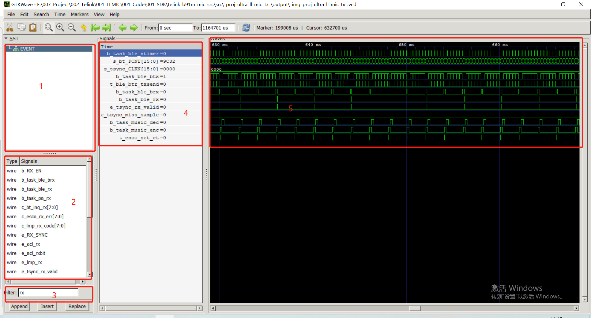
The entire gtkwave tool page is below:
Click EVENT in the first window;
The second window shows the captured signals;
Enter characters in the third window to find signals easily;
The fourth window is for the displayed signal (just double-click on the signal to be displayed in the 2nd window);
The fifth window is the display of the entire signal in terms of time series.
Serial Port VCD Assistant to Generate VCD File
When APP_MODE is configured as APP_MODE_AUDIO_AUTO, it is not possible to use the risc_v_tdb tool to generate a vcd waveform file, and the Serial Port VCD Assistant must be used to generate a VCD waveform file.
First enable the UART_VCD_EN macro in the app_config.h file.
The SDK will call the uart_vcd_init interface in user_init to initialize the corresponding serial port parameters for generating the vcd waveform, with a baud rate of 3000000 and a default TX pin of PD2.
void user_init(void)
{
    ......
#if UART_VCD_EN
    uart_vcd_init(UART0, 3000000, UART0_TX_PD2, UART0_RX_PD3, DMA7);
#endif
    ......
}
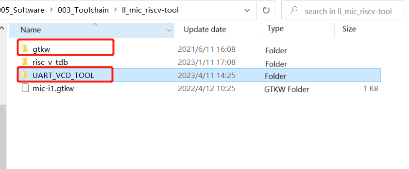
Next, the tool folder UART_VCD_TOOL needs to be placed in the same level directory as the waveform viewing tool gtkw folder (the editor here puts the UART_VCD_TOOL folder directly into the riscv folder).
Use the USB to serial port tool to connect the board and PC, open the serial port VCD assistant risc_v_tdb.exe, click scan, select the corresponding serial port, click open to start generating VCD waveform files.
Where clicking on the VCD is to start/stop grabbing the waveform.
Wave is to view VCD waveform (if log prints ..gtkwave.exe Not Found, the error is caused by the fact that UART_VCD_TOOL and gtkw are not in the same level directory).
Header is the VCD waveform capture header file.
Output is the generated VCD waveform file.
Generic Serial Port View Log
When APP_MODE is configured as APP_MODE_AUDIO_AUTO, it is not possible to use risc_v_tdb tool to view the log, and it is necessary to use usb to serial port tool to view it.
SDK calls app_set_usb_desc_task interface to initialize uart1 with baud rate 1000000 and default pins TX-PE0, RX-PE2.
void app_set_usb_desc_task (int reset)
{
    if (reset)
    {
        .......
        uart1_init(1000000);
        uart_set_tx_dma_config(UART1, DMA5);
        return;
        ......
    }
    ......
}
Use the USB to serial port tool to connect the board and PC, open the usb to serial port tool TL_UART_Log_Tool, click on scan, select the corresponding serial port, click on open to view the log. It is PE0 to output log in the SDK by default.
OTA Tools
OTA Introduction
The OTA function is implemented in BootLoader. After the chip is powered on, the BootLoader program is executed first, and the main flow of BootLoader program is as follows:
(1) Read the value of analog register 0x3c (set to: areg_v_0x3c, after power off and power on, areg_v_0x3c value will be 0x00).
(2) Determine whether areg_v_0x3c is equal to 0x4b. If not, verify APP code, if successfully, jump to execute APP code.
(3) Initialize USB, RF and other functional modules and run BootLoader function.
Support OTA in Two Ways
Mode one: There is a USB port on the RX side and no USB port on the TX side. Either Dongle+RX / Device+TX configuration can be used. By pressing a button, via USB HID, or through other interfaces, issue a command to force both TX and RX into BootLoader mode simultaneously, with RX connected to a computer via USB. The host computer can communicate with RX and upgrade RX through USB, and can upgrade TX through RX.
Mode two: There is no USB port on both RX side and TX side. Configure the Device as both RX and TX. Develop an upgrade board (e.g., using an EVB) to flash Dongle firmware. Upon powering the Dongle, TX or RX can receive commands via buttons/serial port to trigger bootloader entry on the Device. The Dongle will automatically connect to the Device, enabling PC-controlled OTA upgrades for TX and RX modules separately.
Dongle and Device Switching Method
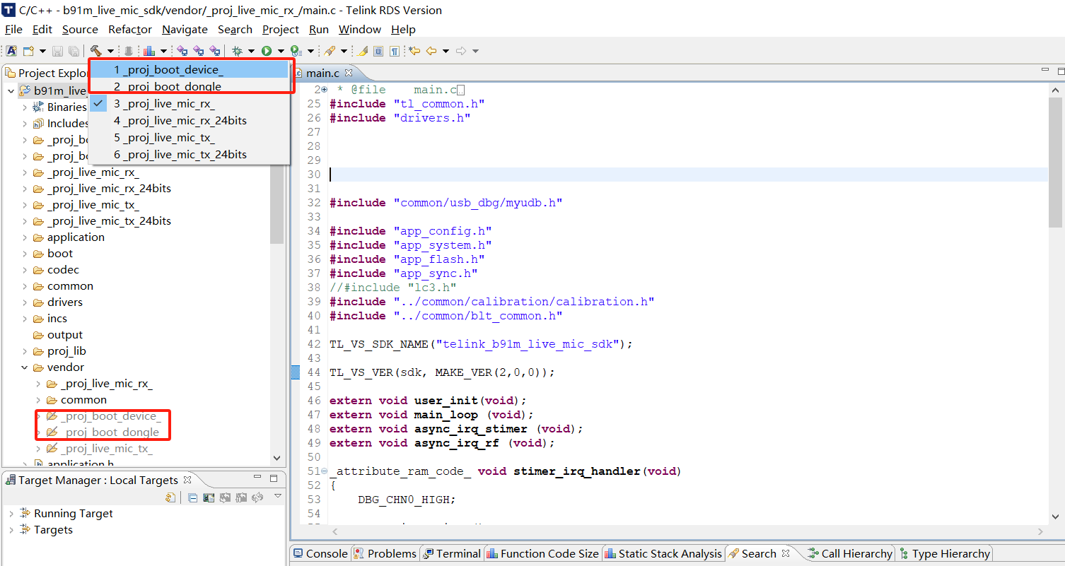
SDK set RX as Dongle and TX as Device by default, which can be changed by modifying the SDK project settings, as shown in the following figure, RX side as Dongle. To set RX as Device, change the red box in the following figure to "_proj_boot_device_\output\proj_boot_device", the same applies to the Tx side.
OTA Procedure
(1) Compile the proj_boot_device and proj_boot_dongle projects.
(2) Open the vendor/_proj_low_latency_mic/app_ui_EVB/app_ui.h file, find the TRANSMIT_DATA_EN macro (create one if there is none), set it to 1, and compile and burn TX and RX respectively.
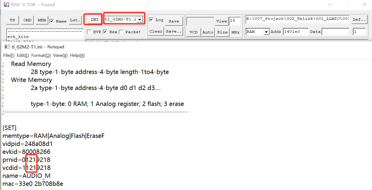
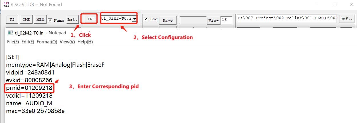
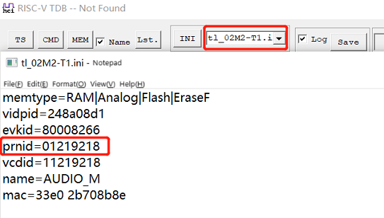
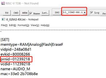
(3) Open 2 RISC-V-TDB tools, select the corresponding ini configuration file respectively, if there is no such file, select an ini file and click the INI button to modify the prnid and vcdid of TX and RX. prnid=01209218, vcdid=11209218 for TX; prnid=01239218, vcdid=11239218 for RX. After setting, reselect the ini file, if 'RISC-V-TDB -- Found' appears in the title bar, and the following log appears, indicating that the settings are correct.
(4) Press SW2 of TX0 and RX at the same time to turn on pairing. After successful pairing, the green or white lights of TX0, TX1 and RX will light up at the same time, indicating successful connection.
(5) As shown in the above figure, at the bottom of the RISC-V-TDB tool corresponding to RX, if the green lights of TX and RX is on, input the command 11 05 00 to upgrade TX0, if the white light is on, input the command 11 05 01 to upgrade TX1, press Enter to send the command, and TX and RX will enter BootLoader respectively after 1 second.
(6) Open usb_ota.exe tool, if the title bar of the tool shows 'DFU Found', it means the Dongle is successfully recognized. As shown in the figure below, if "Remote Device Connected" appears, indicating that the connection between Dongle and Device has been successfully established.
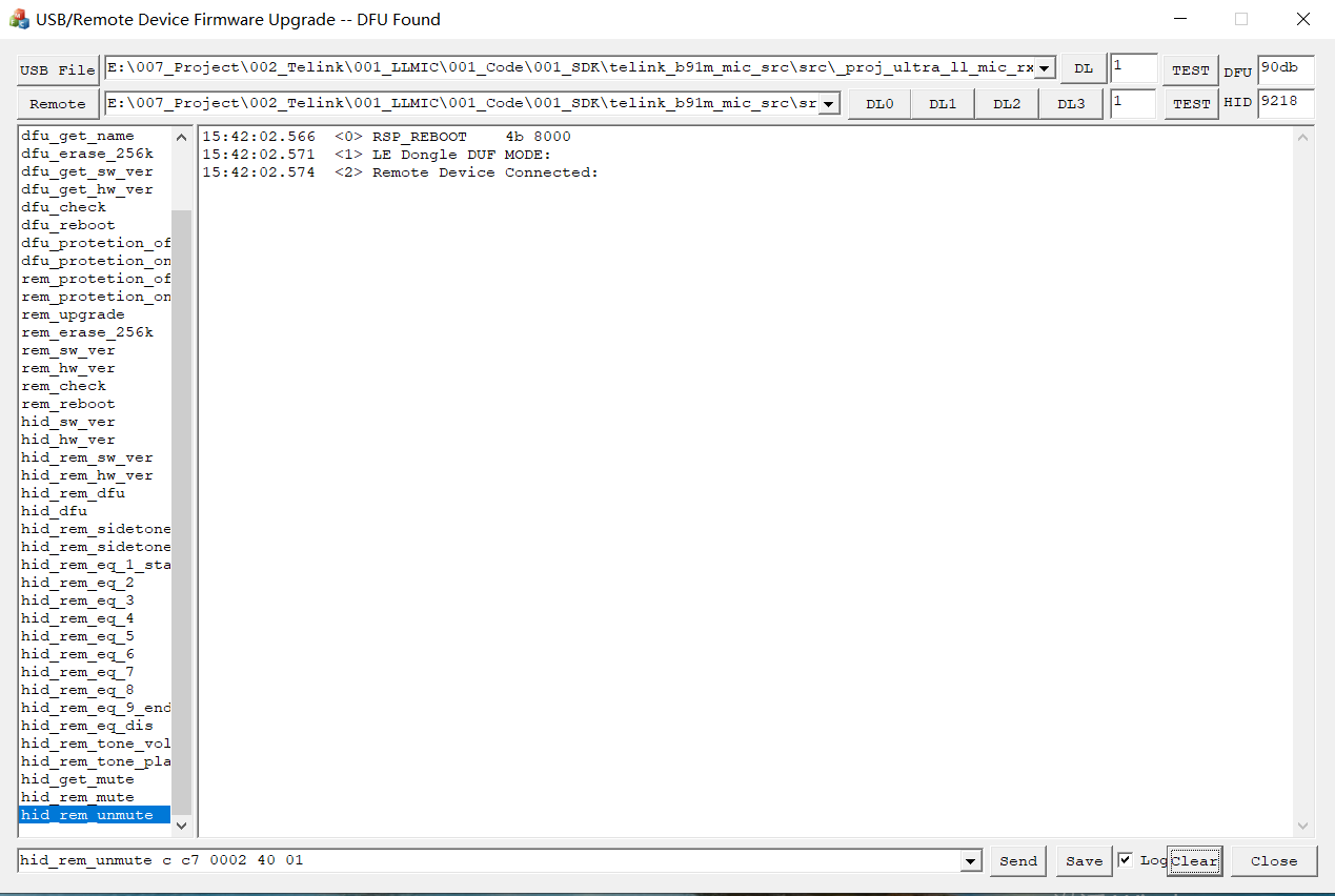
(7) Upgrade Dongle via USB port:
(a) Click the USB File button, and in the file selection box that pops up, select the firmware that needs to be upgraded for Dongle. (b) Click the corresponding DL button on the right side, the following log appears, indicating that Dongle upgrade is successful.
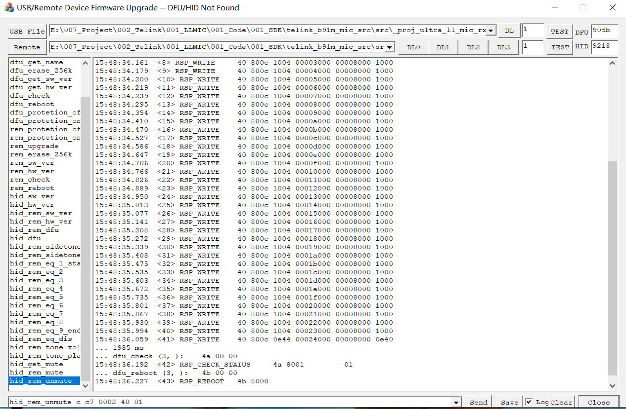
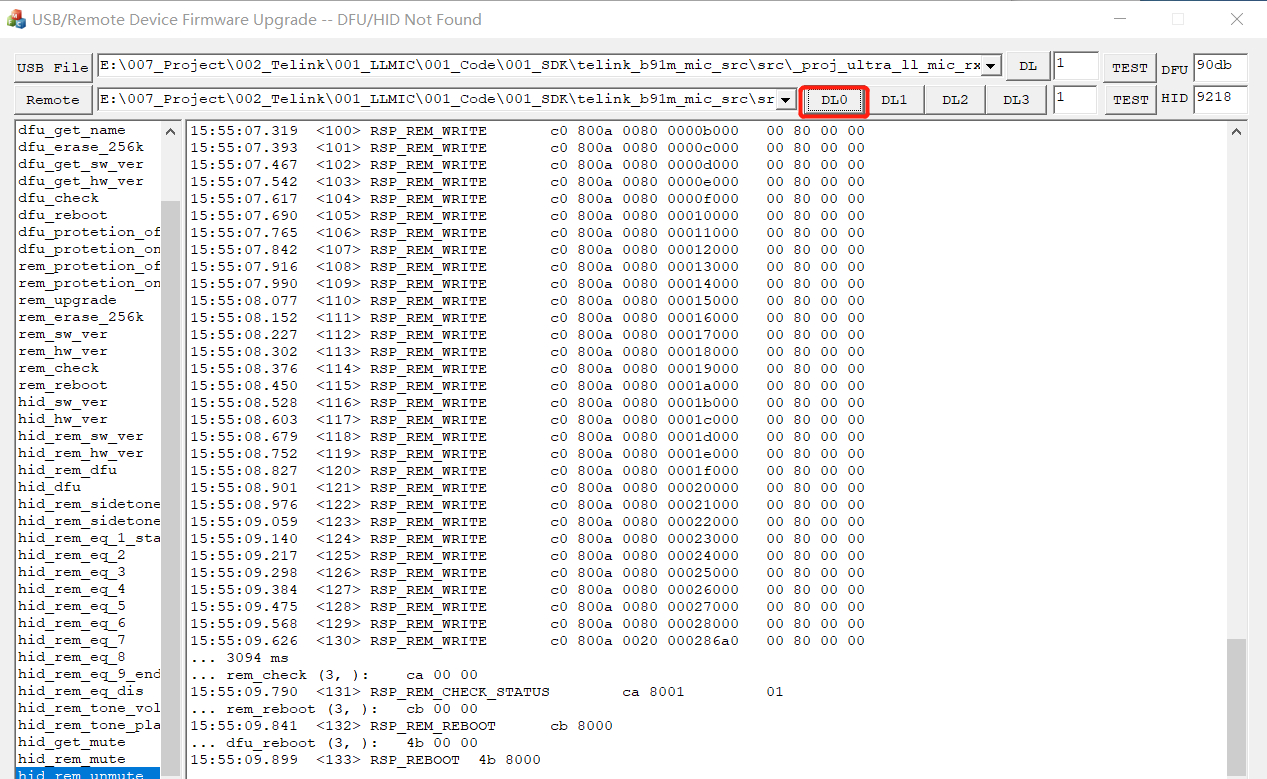
(8) Upgrade the Device (Tx0) via the USB interface:
(a) Click the Remote button, and in the file selection box that pops up, select the firmware that needs to be upgraded for Device. (b) Click the corresponding DL0 button to the right of the Remote button, the following log appears, indicating that the Device is upgraded successfully, then both Dongle and Device will reboot.
(9) To upgrade another TX (TX1):
(a) Burn firmware to TX1 and reset. (b) Re-execute step 4.
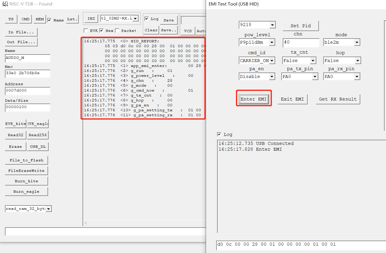
EMI Tool
Introduction to the EMI test tool: Based on USB HID, configure APP_MODE to APP_MODE_DEBUG_HID (the editor here uses this mode, thus combining with the log to explain) or APP_MODE_AUDIO_AUTO, and at the same time, turn on the EMI_TEST_ENABLE macro, in order to enable the EMI test function.
Step 1: Open the emi_test_hid_tool, if it shows USB Connected, the connection is successful.
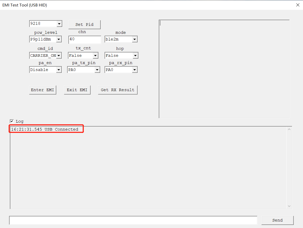
The default pid is 9218, if the pid of the device to be tested has changed, select the corresponding pid in the pid drop-down box and click Set Pid.
Step 2: Configure the EMI parameters, click Enter EMI, as shown in the figure, in the RISC-V TDB tool, it will print "the EMI test has been entered", and print the corresponding configuration parameters.
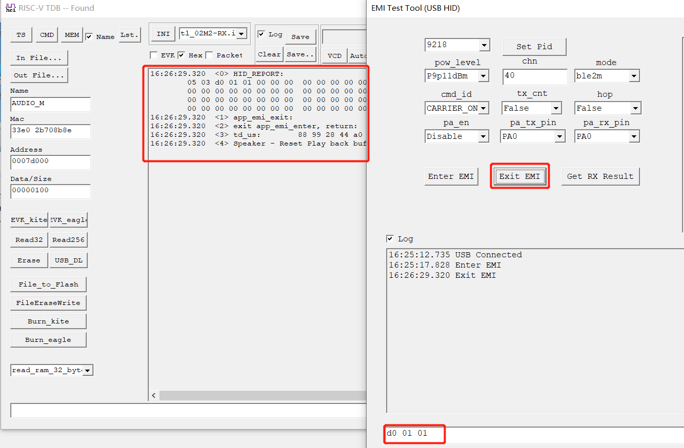
Step 3: Click Exit EMI to exit EMI mode (Note: To modify the configuration, click Exit EMI to exit EMI mode first, and then click Enter EMI to re-enter EMI, so as to realize the configuration modification).
Version Number Tool
SDK will add version number information to the generated BIN based on the version number script during the compilation process, developers can check the version number of the corresponding BIN with the version number tool.
tl_version.h Introduction
MAKE_VER(major, minor, revision) //Used to configure a 24-bit version number, such as 0.0.0

TL_VS_SDK_NAME(str) //Used to refer to the SDK, must be referenced or an error will be reported.

TL_VS_VER(name, value) //Used to configure the version number for the module, optional, generally used for version number definition of algorithm module and codec module.

TL_VS_STRING(name, str) //Used to configure string, optional.

TL_VS_INT(name, value) //Used to configure decimal variables, optional.

TL_VS_HEX(name, value) //Used to configure hexadecimal variables, optional.

TL_VS_BYTE_ARRAY(name, ...) //Used to configure array variables, separated by commas, optional.
Application
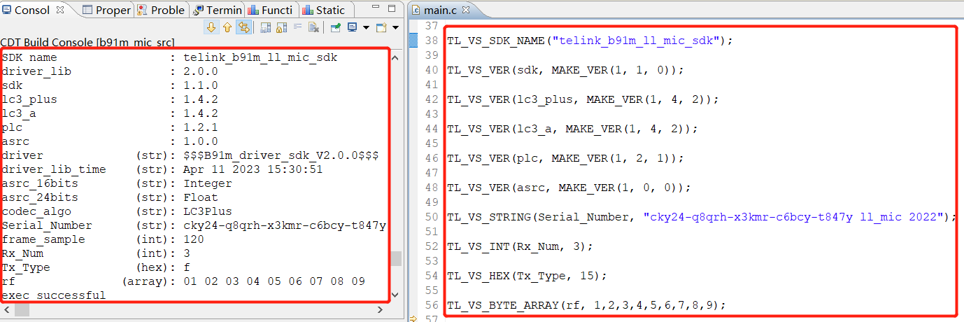
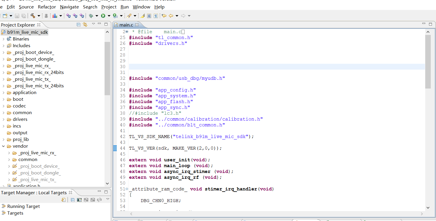
Add the following code to the main.c file in any project:
TL_VS_SDK_NAME("telink_b91m_ll_mic_sdk");

TL_VS_VER(sdk, MAKE_VER(1, 1, 0));

TL_VS_VER(lc3_plus, MAKE_VER(1, 4, 2));

TL_VS_VER(lc3_a, MAKE_VER(1, 4, 2));

TL_VS_VER(plc, MAKE_VER(1, 2, 1));

TL_VS_VER(asrc, MAKE_VER(1, 0, 0));

TL_VS_STRING(Serial_Number, "cky24-q8qrh-x3kmr-c6bcy-t847y ll_mic 2022");

TL_VS_INT(Rx_Num, 3);

TL_VS_HEX(Tx_Type, 15);

TL_VS_BYTE_ARRAY(rf, 1,2,3,4,5,6,7,8,9);
After compiling, version-related information can be displayed in the Compile Options box:
Example
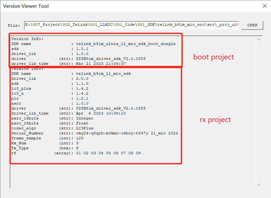
Open the generated bin file such as img_proj_live_mic_rx.bin, the tail address of the hex view is as follows, it can be seen that the version related information are stored to the tail of the bin file:
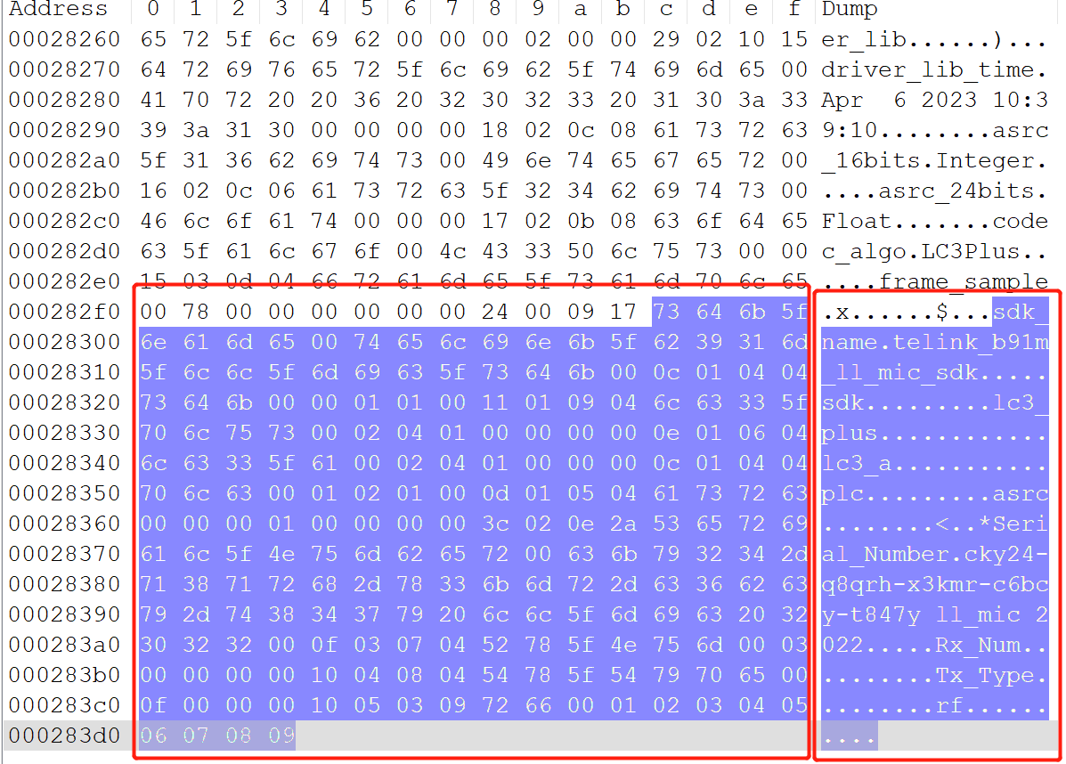
Open VersionViewerTool.exe, click OPEN to select the bin file or directly drag and drop the bin file into the tool box (the first of the two Info appearing is the version number information of the boot project, the second is the version number information of the corresponding project):
Beep Tool
The SDK supports the beep function with ADPCM decoding, so it is needed to convert the customized beep to ADPCM format file by the beep tool.
Users only need to place the customized beep file in WAV format into the tone_tool directory and execute the pcm2adpcm.exe program to generate the beep file tone_adpcm.bin in the sibling directory.
SDK Introduction
Overview
Microphone SDK is generally divided into receiving end and transmitting end based on its functions, hereinafter referred to as TX, RX. Usually TX is the signal sampling end. After sampling, the data will be compressed/encoded, and then sent through the wireless 2.4GHz signal. Take the ultra-low latency SDK as an example, the corresponding projects are _proj_live_mic_tx and _proj_live_mic_240_tx. RX is to receive the data sent from TX side via 2.4GHz signal, decode/decompress the data, and output the audio via USB Audio or Line-out. Take Live Mic SDK for example, the corresponding projects are _proj_live_mic_rx and _proj_live_mic_240_rx.
Software Organization Structure
After the SDK project is imported into the IDE, the file organization is displayed as below. There are 10 top-level folders: algorithm, application, boot, common, drivers, incs, proj_lib, stack, vendor.
algorithm: Algorithm related programs, aes_ccm, crypto, ecc.
application: Provides some general-purpose application handlers, such as print, keyboard, and so on.
boot: Provides the chip's software bootloader, i.e. the assembly process after MCU power on or deepsleep wakeup, to build the environment for the running of the C language program later.
codec: Codec-related algorithms such as filter, resample, etc.
common: Provides some general cross-platform processing functions, such as memory processing functions, string processing functions and so on.
drivers: Provides hardware settings and peripheral drivers that are closely related to MCU, such as clock, flash, I2C, USB, GPIO, UART, and so on.
incs: Public header file directory.
proj_lib: Stores library files necessary for SDK operation (e.g. libB91_driver_i2.a). Files such as the BLE protocol stack, RF driver, PM driver, etc., are encapsulated in the library files, and the user cannot see the source files.
stack: Stores header files related to BLE/BT protocol stack. The source files are compiled into library files that are not visible to the user.
vendor: Stores user application layer code.
boot: Stores the cstartup_9518.S file. cstartup_9518.S: Perform initialization and copying of retention_reset, aes_data, retention_data, ramcode, data, sbss, bss, and stack; initialize flash; set up interrupt vector entries; and implement certain functions that must be written in assembly.
bootlink: The memory layout file, which describes different code sections, placed in flash, I-SRAM, and D-SRAM.
boot.link: The bootlink corresponding to the _proj_boot_xx project.
boot-36k.link: In the vendor's reference project, the configuration difference in this boot linker script is that both the SRAM and corresponding flash addresses are offset by 0x9000 (36KB).
main.c
This file includes the main function entry, system initialization functions, and the infinite loop while(1) writing. It is recommended that this file not be modified in any way and that it be written in its original style (some unimportant code has been omitted).
_attribute_ram_code_ int main(void)
{
    sys_init(DCDC_1P4_LDO_1P8, VBAT_MAX_VALUE_GREATER_THAN_3V6);
    user_read_Flash_value_calib();
    clock_init(PLL_CLK_192M, PAD_PLL_DIV, PLL_DIV2_TO_CCLK, CCLK_DIV2_TO_HCLK, HCLK_DIV2_TO_PCLK, PLL_DIV4_TO_MSPI_CLK);

#if WATCHDOG_ENABLE
    wd_set_interval_ms(15*1000);
    wd_start();
#endif

    clock_cal_24m_rc();

    clock_32k_init(CLK_32K_RC);
    clock_cal_32k_rc(); //6.68ms


    user_init();
    while(1)
    {

        main_loop();
#if WATCHDOG_ENABLE
        wd_clear_cnt();
#endif
    }
    return 0;
}
Configuration File
(1) app_config.h
Application function configuration file for configuring the application function parameters of the entire system, including 2.4GHz-related functions, USB-related functions, audio input functions, and algorithm-related functions.
(2) app_audio_config.h
Audio function configuration file for configuring audio function parameters, including the configuration of encoder, frame length, gain and other related functions.
(3) app_ui.h
UI function configuration file for configuring the UI function parameters, including the configuration of key, led, power detection, beep and other related functions.
The meaning of each parameter in the configuration file will be explained in detail when each module is introduced later.
BootLoader Introduction
BootLoader Projects including TX and RX are proj_boot_device and proj_boot_dongle. They detect the APP firmware integrity after power on and jump to APP execution. Also accessing BootLoader for OTA operation by calling function in APP firmware is available. OTA's operation method can be viewed in OTA Tools.
Telink Live MIC SDK Introduction
SDK Overview
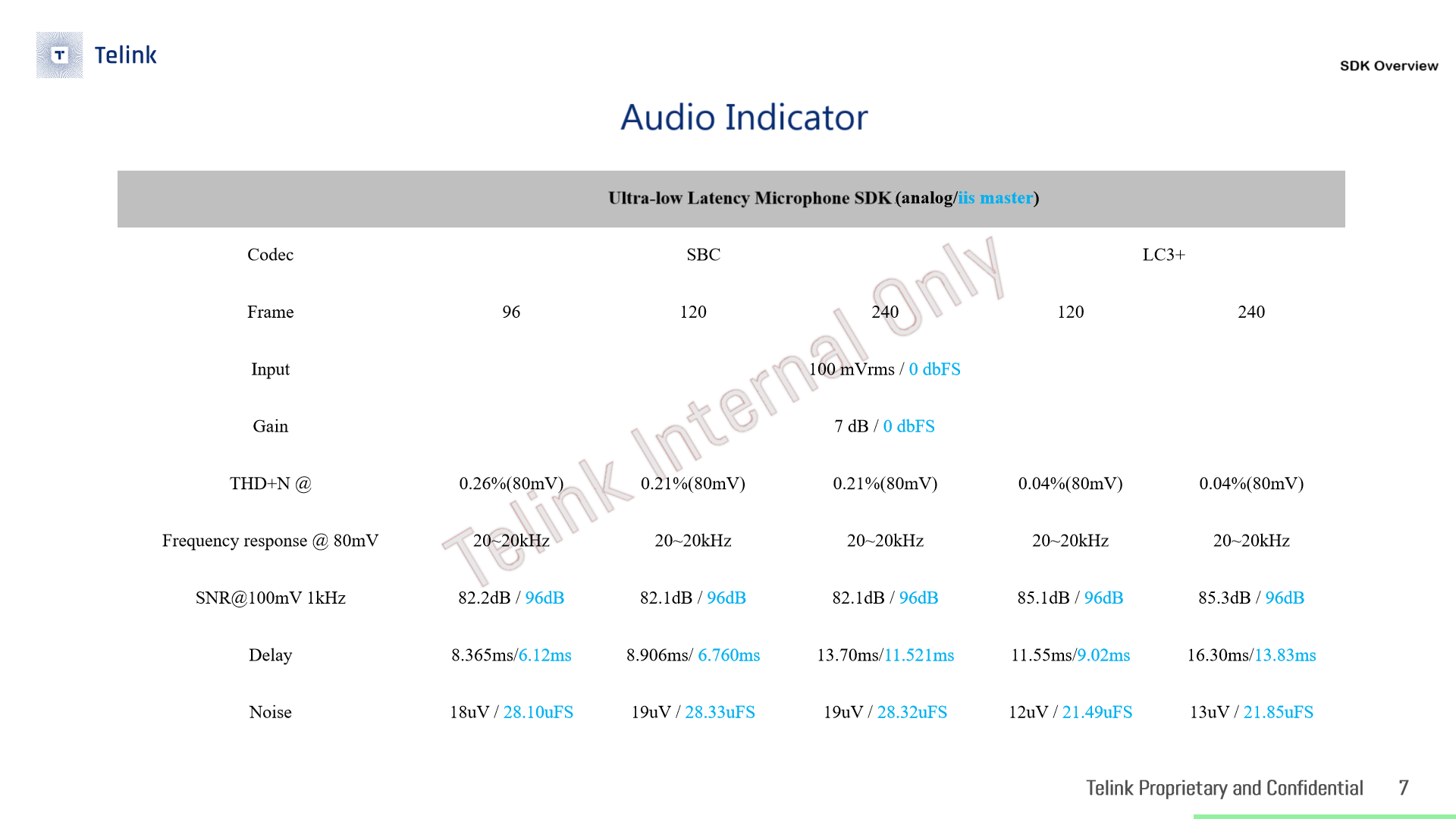
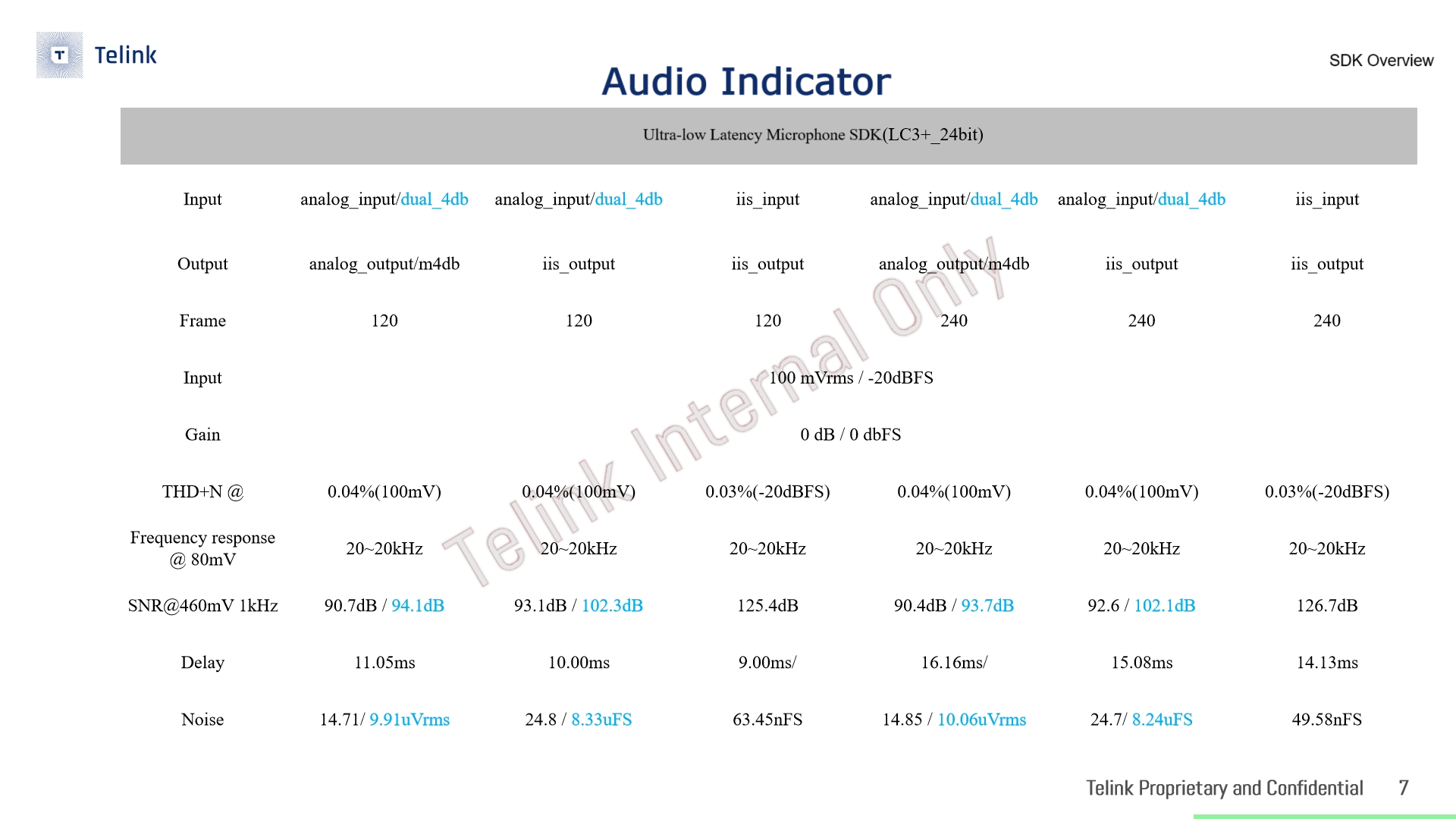
Live MIC supports 2-to-1 and 1-to-1, with low latency, strong anti-interference and other features. Working distance is related to the product form and the number of transmissions, and needs to be tested according to the actual specific product. Typical 2-to-1 audio performance is as follows:
Analog I/O: Latency as low as 17ms (LC3+codec), frequency response 20 ~ 20kHz, THD+N as low as 0.04%, SNR up to 93dB (144dB for 24bit).
IIS I/O: Latency as low as 15ms (LC3+codec), frequency response 20 ~ 20kHz, THD+N as low as 0.04%, SNR up to 96dB (144dB for 24bit).
The SDK provides two project examples, namely: _proj_live_mic_ and proj_live_mic_24bits, as shown below:
The two projects not only differ in size(16bits and 24bits), but also differ in the consumption of some algorithms as well as their functions, as follows:
| Project | _proj_live_mic_ | _proj_live_mic_24bits_ |
|---|---|---|
| LC3+encoding time consuming | 1295 microseconds | 1577 microseconds |
| LC3+decoding time consuming | 993 microseconds | 1269 microseconds |
| USB function | 16bits for both direction | 24bits for uplink only |
The 16bits AP indicators are as follows:
The 24bits AP indicators are as follows (where the blue word dual_4db is the indicator to enable the MIC_DUAL_INPUT_EN function):
SDK Function Introduction
The specific functions of the TX side are as follows:
(1) Supported application-related functions.
(a) USB module: USB HID, USB Debug; (b) Watchdog module; (c) Algorithm module: Include EQ, noise reduction algorithm, resampling algorithm, DRC algorithm; (d) OTA module; (e) EMI module: Support the EMI test command; (f) 2.4GHz module: RF related: 2.4GHz Tx, launch power adaptive, frequency hopping; wireless related: manual pairing, back-connect.
(2) Supported audio-related functions.
(a) Code: LC3+; (b) Audio Input: AMIC, DMIC/AMIC/Line-in or I2S. Audio Output: I2S or Line-out.
(3) Supported UI-related functions.
(a) KEY:Short press, long press, double tap; (b) LED; (c) Power detection.
The UI function of the RX side is the same as that of the TX side, and other functions are as follows:
(1) Supported application-related functions:
(a) USB module: USB Audio upstream and downstream, USB HID, USB Debug; (b) Watchdog module; (c) OTA module: OTA upgrade; (d) EMI module: support EMI fixed frequency testing; (e) 2.4GHz module: RF related: 2.4GHz Rx, frequency hopping, packet error correction; wireless related: manual pairing, reconnect, auto pairing, 1-to-1, 1-to-2, pairing ID filtering.
(2) Supported audio-related functions.
(a) Codec: LC3+; (b) Audio Input: DMIC/AMIC/Line-in or I2S. Audio Output: I2S or Lineout, USB Audio.
Introduction to Key Macros
Many functions of the SDK are controlled by macro switches. The following is a brief introduction to app_config.h, app_audio_config.h, and app_ui.h.
Application-Related Configuration
MIC_TX_NUM:
Default value: 2;
Function description: Control the number of Tx;
Note: The default 2-to-1 mode can be modified to 1-to-1 mode, the time slot becomes shorter and the number of Tx retransmissions increases accordingly.
RF_ERROR_CORRECTION_EN:
Default value: 0;
Function description: Packet error correction function.
APP_MODE:
Default: APP_MODE_DEBUG_ONLY;
Function description: USB mode selection;
Note: The default PRINTER debugging mode can be adjusted to USB HID mode as well as USB Audio.
USB_SPEAKER_ENABLE:
Default value: 1;
Function description: Enable USB Audio downstream;
Note: On by default, can be turned off individually.
USB_MIC_ENABLE:
Default value: 1;
Function description: Enable USB Audio upstream;
Note: On by default, can be turned off individually.
WATCHDOG_ENABLE:
Default value: 1;
Function description: Enable watchdog.
EMI_TEST_ENABLE:
Default value: 0;
Function description: Enable EMI function.
ANT_SWITCH_EN:
Default value: 0;
Function description: Enable Dual antenna switching.
FIELD_STRENGTH_DETECT:
Default value: 0;
Function description: Enable enhancing the anti-interference capability by detecting the environmental signal strength.
OUT_OF_BAND_EN:
Default value: 0;
Function description: Enable out-of-band frequency operation.
APP_NS_ENABLE:
Default value: 0;
Function description: Enable noise reduction function.
APP_WB_NS_ENABLE:
Default: FS_16K_NS_EN;
Function description: The noise reduction function adopts the default mode and supports FS_16K_NS_EN for now.
APP_NS_MODE:
Default value: 1;
Function description: The noise reduction function uses the WebRTC algorithm.
APP_EQ_ENABLE:
Default value: 0;
Function description: Enable EQ function.
ADC_DRC_EN:
Default value: 0;
Function description: Enable DRC function.
UI-Related Configuration
LED_ENABLE:
Default value: 1;
Function Description: Enable LED;
Note: LED_BLUE, LED_GREEN, LED_WHITE, LED_RED are defined respectively.
KEY_ENABLE:
Default value: 1;
Function Description: Enable KEY.
ENABLE_BATT_CHECK:
Default value: 0;
Function description: Enable power detection;
Note: PB3 pin is used by default and can be changed at bat_check_init interface initialization.
Audio-Related Configuration
MIC_DUAL_INPUT_EN:
Default value: 0;
Function description: When it is turned on, the PCM data of left and right mic will be fused and processed, which can obtain better dynamic input, SNR, noise floor and other parameters.
Note: It is needed to merge the left mic input to the right mic in hardware to realize two inputs.
CODEC_DAC_MONO_MODE:
Default value: 1;
Function description: 1: Mono, 0: Stereo;
Note: Lineout on the Tx side is used to monitor the input audio, it is on by default and can be turned off.
CODEC_ALGORITHM_SEL:
Default Value: CODEC_ALGORITHM_LC3A;
Function description: codec selection;
Note: Only LC3+ codec is supported.
LC3A_BIT_RATE:
Default value: 80000;
Function description: LC3+ bitrate;
Note: 96000 80000 are available, the bigger the better the sound quality, the transmission time will be longer and the retransmission will be less.
MIC_SAMPLING_RATE:
Default value: 48000;
Function description: mic sample rate;
Note: Default 48k.
MIC_SAMPLES_PER_PACKET:
Default value: 240 (only 240 is supported);
Function description: mic sample;
Note: Default sampling is 5ms, so one mic sample Samples = 5*48000/1000= 240.
MIC_SLOT_NUM:
Default value: 12;
Function description: The number of times the Tx sends audio packets;
Note: In the 1-to-2 case (1-to-1 is 12), the Tx side retransmits the audio data 12/2 = 6 times per packet, the exact value is affected by the time slot and encoding.
AUDIO_INTERFACE:
Default value: AUDIO_I2S_CODEC;
Function description: CODEC audio source selection;
Note: Default is internal codec input/output, if change to AUDIO_I2S_GPIO, then switch to I2S input/output.
AUDIO_IN_MODE:
Default value: LINE_INPUT;
Function description: Internal codec input source selection;
Note: When AUDIO_INTERFACE is configured as AUDIO_I2S_CODEC, internal codec input source selection can be performed by this macro, which supports AMIC, DMIC, Linein.
AUDIO_INTERFACE_ROLE:
Default value: AUDIO_I2S_AS_MASTER;
Function description: External pin input source master-slave selection;
Note: When AUDIO_INTERFACE is configured as AUDIO_I2S_GPIO, the I2S role can be configured as master/slave with this macro.
CODEC_IN_A_GAIN:
Default value: CODEC_IN_A_GAIN_0_DB;
Function description: Analog input gain;
Note: Used to configure the analog input gain on the Tx and Rx sides.
CODEC_IN_D_GAIN:
Default value:CODEC_IN_D_GAIN_0_DB;
Function description: Digital input gain;
Note: Used to configure the digital input gain on the Tx and Rx sides.
CODEC_OUT_A_GAIN:
Default value:CODEC_OUT_A_GAIN_0_DB;
Function description: Analog output gain;
Note: Used to configure the analog output gain of the Tx and Rx sides.
CODEC_OUT_D_GAIN:
Default value:CODEC_OUT_D_GAIN_0_DB;
Function Description: Digital output gain;
Note: Used to configure the digital output gain of the Tx and Rx sides.
Audio Related
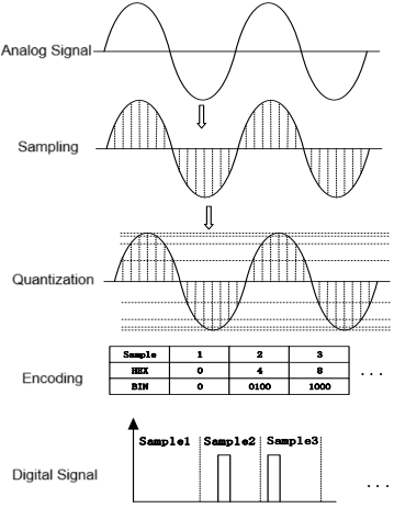
Sampled Audio Basic Concepts
Sampling: Sample the analog signal at regular time intervals.
Quantization: Add a scale to the vertical coordinates and take integer values based on the approximation so that the values of the sample points are all integers.
Encoding: Encode the integer values obtained by quantization in binary.
Digital Signal: Turn the sequence of 0s and 1s obtained by encoding into a high and low level signal.
Pulse Code Modulation (PCM): As seen in the analog-to-digital conversion process above, the content stored in a PCM file is the raw encoded sequence.
Sampling Frequency: Sampling is the digitization of an analog signal on the time axis, and according to Nyquist's theorem (Sampling Theorem), samples are taken (AD converted) at a frequency that is more than twice the highest frequency of the sound. Sounds with frequency between 20Hz ~ 20kHz are recognizable by the human ear. Therefore, the sampling frequency is generally about 40kHz, and common sampling rate for music is 44.1kHz (44,100 samples/s), 48kHz, etc. The sampling rate of telephone is 8kHz.
Number of Sampling Bits: The range of data that each sample point can represent. The number of sampling bits is usually 8bits or 16bits, the larger the number of sampling bits, the more detailed the degree of variation of the recorded sound, and accordingly the larger the amount of data. 16bit is the most common sampling precision.
Number of Channels: The number of channels refers to the independent audio streams that can support different voices, commonly used number of channels are mono, stereo (left and right channels).
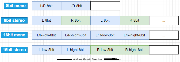
PCM Format
PCM is the uncompressed audio data after sampling and quantization, which is converted from analog signal to standard digital audio data after sampling, quantization and encoding. If it is a mono audio file, the sampled data is stored in chronological order (if it is a dual-channel then it is stored in the LRLR mode), and the storage is also related to the machine's endianness. The little-endian mode is shown in the following figure:
Encoding and Decoding
Supported codec: LC3Plus.
LC3Plus is used for compression and decompression of over-the-air audio transmission.
MCU/SDK Related Functions
Flash Address Space Allocation
Flash stores information in the size of a sector (4KB) as the basic unit, because flash erasure is done also in sector (the erase function is Flash_erase_sector). Theoretically, information of the same type needs to be stored in one sector, and information of different types needs to be in different sectors (to prevent erasing information from other classes by mistake). Therefore, it is recommended that users follow the principle of "different types of information in different sectors" when using flash to store customized information.
The chip supports 1MB of flash as program memory by default. The SDK defines "Flash_SIZE" as 1MB at the end of the boot.link file and determines if "BIN_SIZE" <= "Flash_SIZE", If the user uses flash larger than 1MB, the description needs to be modified accordingly.
Flash is divided into Locked and Unlocked areas according to its function, storing data that does not need to be changed and data that can be changed at any time, respectively. Data that will be changed, such as pairing information, is stored in the Unlocked area, while data that will not be changed, such as firmware, version information, USB_ID, beeps, DRC parameters, EQ parameters, etc., is stored in the Locked area.
(1) The sector 0xFF000 ~ 0xFFFFF stores the MAC address. In fact, the 6 bytes of the MAC address are stored in 0xFF000 ~ 0xFF005, with high byte address stored in 0xFF005, and low byte address in 0xFF000. For example, the contents of flash 0xFF000 to 0xFF005 are 0x11 0x22 0x33 0x44 0x55 0x66 in that order, so the MAC address is 0x665544332211.
Telink's mass production fixture system will burn the MAC address of the actual product to the address 0xFF000, which corresponds to the SDK. If the user needs to change this address, make sure that the fixture system burn-in address is changed accordingly. The SDK will read the MAC address from the CFG_ADR_MAC_1M_Flash address of the flash in the user_init function, this macro can be changed in /vendor/common/blt_common.h.
#ifndef             CFG_ADR_MAC_1M_Flash
#define             CFG_ADR_MAC_1M_Flash              0xFF000
#endif
(2) The two sectors 0xEA000 and 0xEB000 are occupied by the 2.4GHz protocol stack and are used to store pairing information.
(3) In sector 0x00000 ~ 0x3FFFF, 256KB space is used as program space by default. 0x00000 ~ 0x3FFFF totals 256KB for Firmware Storage Space, and 0x40000 ~ 0x7FFFF totals 256KB for storing new firmware during OTA update, i.e. the supported firmware space is theoretically 256KB. For some special reasons, the space at the high address of 0x40000 ~ 0x7FFFF can only be used for 254KB, and the last 4KB cannot be used.
Note
- Actually all of the last 4KB of the high address space cannot be used.
(4) 0xDF000 is the MAC address of the mass production, which is used by default for the MAC address, and only reads the address where 0xFF000 is located if no data is stored at 0xDF000.
(5) 0xDC000 is the EQ data storage address.
(6) 0xDA000 is the USB PID VID storage address.
(7) 0xD9000 is the DRC algorithm data storage address.
(8) 0x80000 is the beep storage address.
(9) 0xFFFF0 is the USB_ID storage address.
(10) All the remaining flash space is used as data storage space for users.
User Flash Management Function
When users need to develop flash-related functions that are frequently read and written, such as volume, shutdown time and other SDK pairing information, it is recommended to use the flash management function provided by SDK, which can open a section of the specified address dedicated to user-defined flash content management, and can achieve the following advantages:
(1) Flash Management: When writing data within the user-specified address region, the system starts from the beginning. Upon reaching the end of the region, it erases the entire area and resumes writing from the start again. This cyclic process enhances flash lifespan and utilization efficiency while reducing erase operations.
(2) Same data will not be written: when calling the write flash interface of the flash management module, it will compare the written content in the flash, and if it is the same, it will not be written.
(3) Data verification: data will be verified before written, if the verification does not pass, it will not be written to prevent wrong writing.
(4) Data Backup Function: When Flash_STORAGE_BACKUP_EN is on (default off), half of the specified flash area will be used for backup, to prevent data loss problems caused by power down when flash is erased and ready to be written.
Introduction to Flash Management Main Functions
Flash_storage_init (Flash_storage_t *fs, u32 addr, u8 *item_ptr, u16 item_size): Initialisation function for flash read/write functions. In addition to initializing the flash read/write functions, it will also read the flash data into a customized data structure. The first parameter is the address of a structure associated with this function, the second parameter is the flash address to be read and written to, the third parameter is the address of the customized data structure, and the fourth parameter is the length of the customized data structure.
Flash_storage_write (Flash_storage_t *fs): Function interface that writes to flash. Called to write data from a customized structure to flash. The parameter is the address of a structure associated with this feature.
Flash_storage_read (Flash_storage_t *fs): Function interface that reads flash. Since Flash_storage_init calls this function when itself is called, i.e. the initialisation will read the flash data into a customized data structure. So this function is not needed to call in general.
Operation Flow of Flash Management Function
Above is the introduction of the functions related to flash read/write, below takes the SDK pairing information as an example to introduce how to operate.
(1) Firstly, define a pairing information Flash_storage_t structure (global variable) fs_pair_info. Next, define the pairing information pair_info_s structure (divided into TX and RX) pair_info as follows:
typedef struct {
    u32 access_code;
#if APP_BUILD == APP_MIC_RX
    u32 slave_ids[REMOTE_DEVICE_NUM_MAX];                     //<! for RX
    u8  remote_mac[REMOTE_DEVICE_NUM_MAX][LOCAL_MAC_LEN];     //<! for RX
    u8  lp_dev_id;                                            //<! for RX, last paired dev id.
#else
    u8  remote_mac[LOCAL_MAC_LEN];                            // for TX
    u8  dev_id;
#endif
    u8  connect_chn;
    u8  valid;
} pair_info_s;

pair_info_s pair_info;
Flash_storage_t fs_pair_info;
(2) Call Flash_storage_init (four-byte alignment) in the app_user_data_init interface for fs_pair_info initialisation and pair_info binding as follows:
void app_user_data_init(void)
{
    ......
    Flash_storage_init(&fs_pair_info, Flash_SYS_USER_BASE, (u8 *)&pair_info, sizeof(pair_info));
    if (!pair_info.valid) {
        tmemset(&pair_info, 0, sizeof(pair_info));
    }
    ......
}
This step reads the pairing information stored in the flash at the address corresponding to Flash_SYS_USER_BASE into pair_info (when initialised for the first time, the contents of the flash are all FF, and since the valid value in the pair_info_s structure is not legal, all the values in pair_info are set to 0).
(3) When TX and RX complete the pairing process, regardless of TX or RX, pair_info will be updated accordingly, and finally call Flash_storage_write in the app_user_data_update interface to write the updated initial value of the pair_info with the header of Flash_storage_header_s to the flash, as shown below:
typedef struct {
    u16 version;                                         /**< Version of data. */
    u16 length;                                          /**< Length of data, exclude header(version, length, verify). */
    u32 verify;                                          /**< Verify of data. */
} Flash_storage_header_s;

void app_user_data_update(void)  // user data information changed, call this func write to flash
{
    pair_info.valid = PAIR_INFO_VALID_BYTE;
    Flash_storage_write(&fs_pair_info);     /* push buffer into flash */
}
(4) Take the pairing process of TX0 (mac address: 22 11 22 33 44 55), TX1 (mac address: 11 11 22 33 44 55) and RX (mac address: 33 11 22 33 44 55) as an example:
After TX0 and RX are paired for the first time, the contents of the 0xEB000 address are read through the risc-v tool as follows.
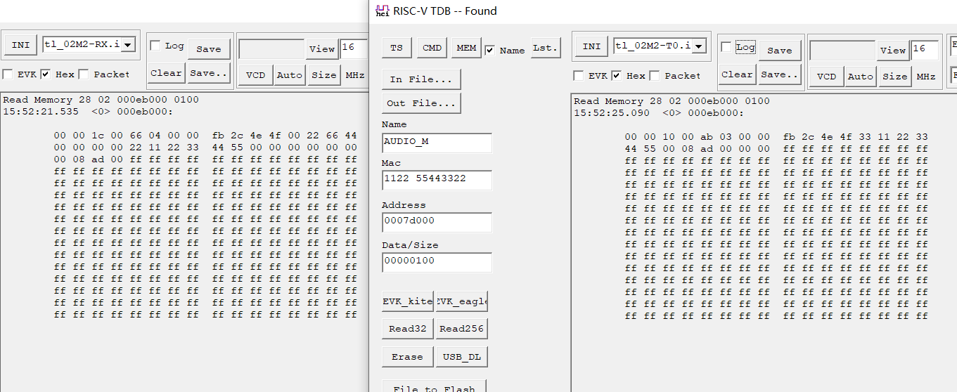
In the TX0 pairing information:
- 0~1 bytes: version in Flash_storage_header_s, refers to the data version number, currently undefined, default is 0x0000.
- 2~3 bytes: length in Flash_storage_header_s, refers to the length of the pairing information stored by TX0 as 0x0010, which is 16 bytes.
- 4~7 bytes: a 4-byte verify in Flash_storage_header_s, refers to the checksum value of the entire storage information as 0x000003ab.
- 8~11 bytes: access_code value is 0x4f4e2cfb.
- 12~17 bytes: remote_mac, refers to the corresponding mac address of the paired RX device as 33 11 22 33 44 55.
- 18 byte: dev_id value is 0x00, refers to TX0 current device id.
- 19 byte: connect_chn value is 0x08 and refers to the sequence value corresponding to the paired channel.
- 20 byte: valid value is 0xad, legal.
- 21~23 bytes: for four-byte alignment.
In the RX pairing information:
- 0~1 bytes: version in Flash_storage_header_s, refers to the data version number, currently undefined, default is 0x0000.
- 2~3 bytes: length in Flash_storage_header_s, refers to the length of the pairing information stored by Rx as 0x001c, which is 28 bytes.
- 4~7 bytes: a 4-byte verify in Flash_storage_header_s, refers to the checksum value of the entire storage information as 0x00000466.
- 8~11 bytes: access_code, value is 0x4f4e2cfb.
- 12~15 bytes: slave_ids of TX0, refers to the corresponding slave id of the paired TX0 device as 0x44662200.
- 16~19 bytes: slave_ids of TX1, refers to the corresponding slave id of the paired TX1 device, the value is 0x00000000 since it is unpaired.
- 20~25 bytes: remote_mac of TX0, refers to the corresponding mac address of the paired TX0 device as 22 11 22 33 44 55.
- 26~31 bytes: remote_mac of TX1, refers to the corresponding mac address of the paired TX1 device, the value is 0x00000000 since it is unpaired.
- 32 byte: lp_dev_id, refers to the last paired device id as 0x00 (the device id of TX0 is stored here).
- 33 byte: connect_chn value is 0x08 and refers to the sequence value corresponding to the paired channel.
- 34 byte: valid value is 0xad, legal.
- 35 byte: for four-byte alignment.
Pairing TX1 and RX on the basis that TX0 and RX are already paired. Due to the addition of Tx1-related information in RX pairing information pair_info, the pairing information in the flash is updated, that is, on the basis of the pairing information corresponding to the previous TX0, offset to the next address, read the 0xEB000 address through the risc-v tool as follows:
In the TX1 pairing information:
- 0~1 bytes: version, default is 0x0000.
- 2~3 bytes: length, refers to the length of the pairing information stored by TX1 as 0x0010, which is 16 bytes.
- 4~7 bytes: verify, 0x000003ac.
- 8~11 bytes: access_code value is 0x4f4e2cfb.
- 12~17 bytes: remote_mac, refers to the corresponding mac address of the paired RX device as 33 11 22 33 44 55.
- 18 byte: dev_id value is 0x01, refers to current TX1 device id.
- 19 byte: connect_chn value is 0x08 and refers to the sequence value corresponding to the paired channel.
- 20 byte: valid value is 0xad, legal.
- 21~23 bytes: for four-byte alignment.
In the RX pairing information:
- 36~37 bytes: version, default is 0x0000.
- 38~39 bytes: length, refers to the length of the pairing information stored by Rx as 0x001c, which is 28 bytes.
- 40~43 bytes: verify, refers to the checksum value of the entire storage information as 0x00000665.
- 44~47 bytes: access_code, value is 0x4f4e2cfb.
- 48~51 bytes: slave_ids of TX0, refers to the corresponding slave id of the paired TX0 device as 0x44662200.
- 52~55 bytes: slave_ids of TX1, refers to the slave id corresponding to the paired TX1 device as 0x44552233.
- 56~61 bytes: remote_mac of TX0, refers to the corresponding mac address of the paired TX0 device as 22 11 22 33 44 55.
- 62~67 bytes: remote_mac of TX1, refers to the corresponding mac address of the paired TX1 device as 11 11 22 33 44 55.
- 68 byte: lp_dev_id, refers to the last paired device id of 0x01 (the device id of TX1 is stored here).
- 69 byte: connect_chn value is 0x08, refers to the sequence value corresponding to the paired channel.
- 70 byte: valid value is 0xad, legal.
- 71 byte: for four-byte alignment.
Note
- The Flash_storage_t structure fs_pair_info is bound to the pairing information structure pair_info after initialization. It is the pair_info that operates on the data, and it is only when the Flash_storage_write interface is called after a change in the pair_info (comparing the information stored in flash) that the Flash_storage_t structure fs_pair_info undergoes address offset and eventually writes the updated pair_info to the offset address in the flash.
Wireless Audio Transmission
LE 2M Phy is used in the SDK application. The physical layer transmission rate is 2M bit/s, i.e., it takes 4µs to transmit a byte. LinkLayer users need to have a certain understanding of telink's RF driver. However, because the RF peripheral content is too much, this chapter only outlines the RF interface function used in sdk. Please refer to the driver handbook through the telink wiki for more information.
Audio Streaming Procedure
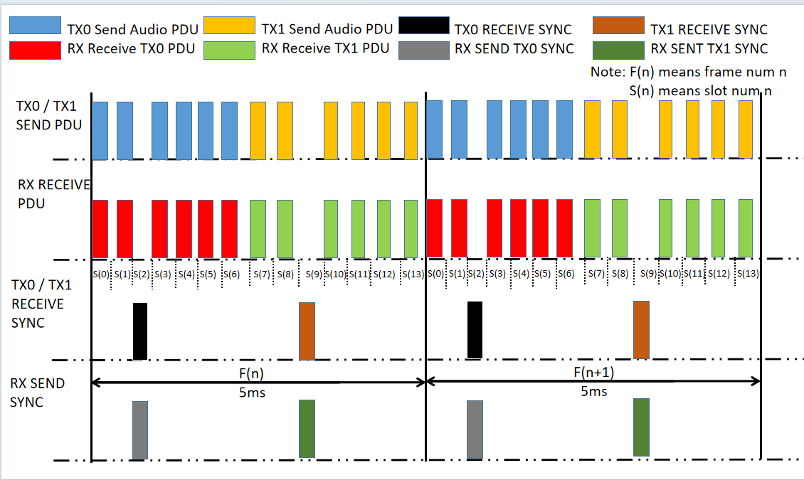
The entire audio stream is broadcast + ACK mechanism. TX will send 2 audio packets first, RX will return a normal ACK when it receives the packets, if TX can't receive that ACK, it will continue to send the remaining audio packets, which do not need ACK. Using 5ms for a frame data, and then divide into N slot interval for sending and receiving packets in each frame data. 2 to 1 and 1 to 1 examples are configured with different N values, such as _proj_live_mic_projects using LC3 + coding configuration of N for 12/2 = 6. When coding and decoding, RX will decode the previously received audio packets at a fixed slot, and TX will encode the current audio packet at a fixed slot, which ensures that the transmission delay of the entire audio data stream remains unchanged.
(1) 5ms frame length, LC3+, 2-to-1 mode
1 frame is 5ms, and a further 14 slot intervals are divided in each frame for sending and receiving packets (12 audio packets).
Where slot 2 is a synchronisation channel for RX transmission of information such as TX hopping frequency table, pairing/reconnection, other control commands, and so on.
slot 0 ~ slot 1 and slot 3 ~ slot 6 are TX0 packet sending slot.
Where slot 2 is the synchronization packet reception slot for TX0.
Slot 7 ~ slot 8 and slot 10 ~ slot 13 are TX1 packet sending slot.
where slot 9 is the synchronization packet reception slot for TX1.
(2) 2.5ms frame length, LC3+, 1-to-1 mode
1 frame is 5ms, and 13 more slot intervals are divided in each frame for sending and receiving packets (12 audio packets).
slot 0 ~ slot 1 and slot 3 ~ slot 13 are TX0 packet sending slot.
where slot 2 is the synchronization packet reception slot for TX0.
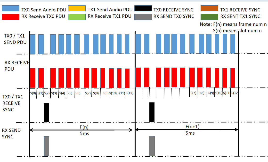
Note
- Compared to the 2-to-1 mode, in the 1-to-1 mode, the number of TX retransmissions is 6 times more because there is only 1 transmitter, but the decoding position is adjusted to the decoding position of TX1 in the 2-to-1 mode, so the transmission distance becomes farther while the latency is increased by about 2.5ms.
RF Main Function Description
async_init: Initialise system timer, initialise RF, frequency hopping, timing parameters and individual interrupts;
async_stx_start: RF packet sending function;
async_srx_start: RF packet receiving function;
async_irq_rf: RF interrupt handler function.
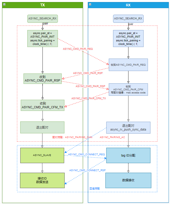
Scanning and Connection Process
Pairing Process
Low Power Management
The MCU is in working mode when it executes the programme normally, and the working current is between 3 ~ 7mA at this time. Enter the low power mode to save power consumption.
Low power mode, also known as sleep mode, consists of three types: suspend mode, deepsleep mode and deepsleep retention mode.
Deepsleep Mode
SDK currently supports deepsleep mode, in which the programme stops running, most of the MCU hardware modules are powered off, and the PM hardware modules keep working. In deepsleep mode IC current is less than 1µA, if the standby current of the built-in flash is around 1µA, it may cause the measured deepsleep current to be 1 ~ 2µA. When deepsleep mode is wake_up, the MCU will restart, similar to the effect of powering up, and the program will restart to initialise. The program will restart to initialise.
In Deepsleep mode, except for a few registers on the analog register that can save the state, all other Sram, digital register and analog register are powered down and lose their state.
PM module specialized non-volatile analog register: The DEEP_ANA_REG defined in drivers/B91/pm.h, as shown in the following code:
#define PM_ANA_REG_POWER_ON_CLR_BUF0    0x39 // initial value 0x00. [Bit0][Bit1] is already occupied. The customer cannot change!
#define PM_ANA_REG_POWER_ON_CLR_BUF1    0x3a // initial value 0x00
#define PM_ANA_REG_POWER_ON_CLR_BUF2    0x3b // initial value 0x00
#define PM_ANA_REG_POWER_ON_CLR_BUF3    0x3c // initial value 0x00
#define PM_ANA_REG_POWER_ON_CLR_BUF4    0x3d // initial value 0x00
#define PM_ANA_REG_POWER_ON_CLR_BUF5    0x3e // initial value 0x00
#define PM_ANA_REG_POWER_ON_CLR_BUF6    0x3f // initial value 0x0f
#define PM_ANA_REG_POWER_ON_CLR_BUF7    0x38 //initial value =0xff
The registers above 0x3f will only recover their initial values on power down. Note that users are not allowed to use ANA_REG_0x39, this analog register is reserved for use for the underlying stack. If the application level code uses this register, it needs to be modified to ana_3a ~ ana_3f. Because there is limited analog retention registers, it is recommended that users use each bit to indicate a different status bit information.
0x38 register can be initialised in three cases: hardware/software reset, power down and watchdog, it should be noted that bit0 has been used by stack, users need to avoid this bit when using it.
Users can use the return value of API pm_get_mcu_status(void) after sys_init(power_mode_e power_mode) to determine from which state the cpu is returning, the return value is as follows:
typedef enum{
MCU_STATUS_POWER_ON = BIT(0),
MCU_STATUS_REBOOT_BACK = BIT(2), //the user will not see the reboot status.
MCU_STATUS_DEEPRET_BACK = BIT(3),
MCU_STATUS_DEEP_BACK = BIT(4),
MCU_STATUS_REBOOT_DEEP_BACK = BIT(5), //reboot + deep
}pm_mcu_status;
Low-Power Wake-Up Source
suspend/deepsleep/deepsleep retention can all be woken up by GPIO PAD and timer. This SDK only focuses on 2 kinds of wakeup sources, as shown below (note that the definitions of PM_TIM_RECOVER_START and PM_TIM_RECOVER_END in the code are not wakeup sources):
typedef enum {
Telink B91 BLE Single Connection SDK Developer Handbook
AN-20111001-C2 217 Ver.0.2.0
PM_WAKEUP_PAD = BIT(3),
PM_WAKEUP_TIMER = BIT(5),
}SleepWakeupSrc_TypeDef;
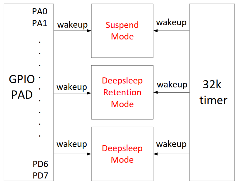
As shown above, deepsleep mode has 2 wake-up sources in hardware: TIMER, GPIO PAD.
The wakeup source PM_WAKEUP_TIMER comes from the hardware 32k timer (32k RC timer or 32k Crystal timer). 32k timer has been initialised correctly in the SDK and it is not needed to configure anything to use it, just set this wakeup source in cpu_sleep_wakeup().
The wake-up source PM_WAKEUP_PAD comes from the GPIO module, and the high and low levels of all GPIOs (PAx/PBx/PCx/PDx/PEx) except the 4 MSPI pins have wake-up functions.
Configure the API for GPIO PAD wake-up sleep mode:
typedef enum{
    WAKEUP_LEVEL_LOW        = 0,
    WAKEUP_LEVEL_HIGH       = 1,
}pm_gpio_wakeup_level_e;
void pm_set_gpio_wakeup (gpio_pin_e pin, pm_gpio_wakeup_Level_e pol, int en);
#define cpu_set_gpio_wakeup pm_set_gpio_wakeup
Pin is the GPIO definition.
Pol is the wake-up polarity definition: Level_High means high level wake-up, Level_Low means low level wake-up.
EN: 1 means enable, 0 means disable.
Example:
cpu_set_gpio_wakeup (GPIO_PC2, Level_High, 1); //Enable GPIO_PC2 PAD wakeup, high-level wakeup
cpu_set_gpio_wakeup (GPIO_PC2, Level_High, 0); //Disable GPIO_PC2 PAD wakeup
cpu_set_gpio_wakeup (GPIO_PB5, Level_Low, 1);  //Enable GPIO_PB5 PAD wakeup, low-level wakeup
cpu_set_gpio_wakeup (GPIO_PB5, Level_Low, 0);  //Disable GPIO_PB5 PAD wakeup
Meanwhile, in the UI definition of the EVB, within the app_key_scan_init interface of the app_key.c file, pm_set_gpio_wakeup is called to configure all key-corresponding pins with wake-up enabled, using a high level for wake-up:
void app_key_scan_init(void)
{
    ......
    for(int i=0;i<MATRIX_ROW_COUNT;i++) {
        gpio_pin_e pin = matrix_row_pins[i];
        gpio_set_input_en(pin, 1);
        gpio_set_output_en(pin, 0);
        gpio_setup_up_down_resistor(pin, PM_PIN_PULLDOWN_100K);
    pm_set_gpio_wakeup(pin, WAKEUP_LEVEL_HIGH, 1);
    }
    ......
}
Low Power Mode Entry and Wake-Up
Set the API for the MCU to go to sleep and wake up as:
typedef int (*cpu_pm_handler_t)(SleepMode_TypeDef sleep_mode, SleepWakeupSrc_TypeDef wakeup_src, unsigned int
wakeup_tick);
cpu_pm_handler_t cpu_sleep_wakeup;
The first parameter sleep_mode: there are 4 choices to set the sleep mode, which are suspend mode, deepsleep mode, deepsleep retention 32K Sram, and deepsleep retention 64K Sram.
typedef enum {
//available mode for customer
SUSPEND_MODE = 0x00,
DEEPSLEEP_MODE = 0x30,
DEEPSLEEP_MODE_RET_SRAM_LOW32K = 0x21, //for boot from sram
DEEPSLEEP_MODE_RET_SRAM_LOW64K = 0x03, //for boot from sram
DEEPSLEEP_MODE_RET_SRAM = 0x21,
//not available mode
DEEPSLEEP_RETENTION_FLAG = 0x0F,
}SleepMode_TypeDef;
The second parameter wakeup_src: set the current wakeup source for suspend/deepsleep, the parameter can only be one or more of PM_WAKEUP_PAD, PM_WAKEUP_TIMER. If wakeup_src is 0, then it cannot be woken up after entering low power sleep mode.
The third parameter wakeup_tick: When PM_WAKEUP_TIMER is set in wakeup_src, it is needed to set wakeup_tick to determine when the timer will wake up the MCU. If PM_WAKEUP_TIMER wakeup is not set, this parameter is meaningless. The value of wakeup_tick is an absolute value, which needs to be set according to the System Timer tick introduced earlier in this document. When the value of System Timer tick reaches the set wakeup_tick, sleep mode is woken up. The value of wakeup_tick needs to add the absolute time converted from the time needed to sleep based on the current System Timer tick value, in order to effectively control the sleep time. If the wakeup_tick is set directly without considering the current System Timer tick, the timing of the wakeup is uncontrollable. Since wakeup_tick is an absolute time and must be within the range that a 32bit System Timer tick can represent, the maximum sleep time that this API can represent is limited. The current design is that the maximum sleep time is 7/8 of the largest corresponding time of the System Timer tick that can be represented by the 32bit. The maximum time System Timer tick can represent is about 268s, so the longest sleep time is 268*7/8=234s, i.e., the following delta_Tick can't be more than 234s, and user can call long sleep function if longer sleep time is needed.
cpu_sleep_wakeup(SUSPEND_MODE, PM_WAKEUP_TIMER, clock_time() + delta_tick);
The return value is the set of wake-up sources of the current sleep mode, and the wake-up source indicated by each bit of the return value is:
typedef enum {
WAKEUP_STATUS_COMPARATOR = BIT(0),
WAKEUP_STATUS_TIMER = BIT(1),
WAKEUP_STATUS_CORE = BIT(2),
WAKEUP_STATUS_PAD = BIT(3),
WAKEUP_STATUS_MDEC = BIT(4),
STATUS_GPIO_ERR_NO_ENTER_PM = BIT(7),
STATUS_ENTER_SUSPEND = BIT(30),
}pm_wakeup_status_e;
(a) When WAKEUP_STATUS_TIMER bit is 1, indicating that the current sleep mode is woken up by Timer.
(b) When WAKEUP_STATUS_PAD bit is 1, indicating that the current sleep mode is woken up by GPIO PAD.
(c) When both WAKEUP_STATUS_TIMER and WAKEUP_STATUS_PAD are 1, indicating that both Timer and GPIO PAD wake-up sources are active at the same time.
(d) STATUS_GPIO_ERR_NO_ENTER_PM is a specific status indicating that a GPIO wake-up error has occurred, where a GPIO PAD configured for high-level wake-up is already at a high level when the cpu_sleep_wakeup function is called to enter suspend mode and the PM_WAKEUP_PAD wake-up source is enabled, causing the system to fail to enter suspend mode and the MCU to immediately exit the cpu_sleep_wakeup function, thus returning the value STATUS_GPIO_ERR_NO_ENTER_PM.
The following forms of sleep control are generally used:
cpu_sleep_wakeup (SUSPEND_MODE , PM_WAKEUP_TIMER, clock_time() + delta_Tick);
The delta_Tick is a relative time (e.g. 100* CLOCK_16M_SYS_TIMER_CLK_1MS), which becomes absolute when added to the current clock_time().
Example of cpu_sleep_wakeup usage:
cpu_sleep_wakeup (SUSPEND_MODE , PM_WAKEUP_PAD, 0);
The programme enters suspend mode when executing this function and can only be woken up by the GPIO PAD.
cpu_sleep_wakeup (SUSPEND_MODE , PM_WAKEUP_TIMER, clock_time() + 10* CLOCK_16M_SYS_TIMER_CLK_1MS);
When the programme executes this function, it enters suspend mode and can only be woken up by Timer, the wake-up time is the current time plus 10ms, so the suspend time is 10ms.
cpu_sleep_wakeup (SUSPEND_MODE , PM_WAKEUP_PAD | PM_WAKEUP_TIMER,clock_time() + 50* CLOCK_16M_SYS_TIMER_CLK_1MS);
When the programme executes this function, it enters suspend mode and can be woken up by GPIO PAD and Timer, and the time for Timer to wake up is set to 50ms. If the wake-up action of GPIO is triggered before the end of 50ms, the MCU will be woken up by GPIO PAD; if there is no action of GPIO within 50ms, the MCU will be woken up by Timer.
cpu_sleep_wakeup (DEEPSLEEP_MODE, PM_WAKEUP_PAD, 0);
The programme enters deepsleep mode when executing this function and can be woken up by the GPIO PAD.
cpu_sleep_wakeup (DEEPSLEEP_MODE_RET_SRAM_LOW32K , PM_WAKEUP_TIMER, clock_time() + 8*
CLOCK_16M_SYS_TIMER_CLK_1S);
The programme enters deepsleep retention 32K Sram mode when executing this function, and can be woken up by Timer, the wake-up time is 8s after executing this function.
cpu_sleep_wakeup (DEEPSLEEP_MODE_RET_SRAM_LOW32K , PM_WAKEUP_PAD | PM_WAKEUP_TIMER,clock_time() + 10*
CLOCK_16M_SYS_TIMER_CLK_1S);
When the programme executes this function, it enters deepsleep retention 32K Sram mode, and can be woken up by GPIO PAD and Timer, and the Timer wake-up time is 10s after executing this function. If the GPIO action is triggered before the end of 10s, MCU can be woken up by GPIO PAD; if there is no GPIO action within 10s, MCU can be woken up by Timer.
Operation Flow after Low-Power Wake-Up
When the user calls the API cpu_sleep_wakeup, the MCU enters sleep mode; when the wakeup source triggers the MCU to wake up, the software operation flow of the MCU varies for different sleep modes.
The following describes in detail the MCU operation flow after deepsleep is woken up. Please refer to the following figure.
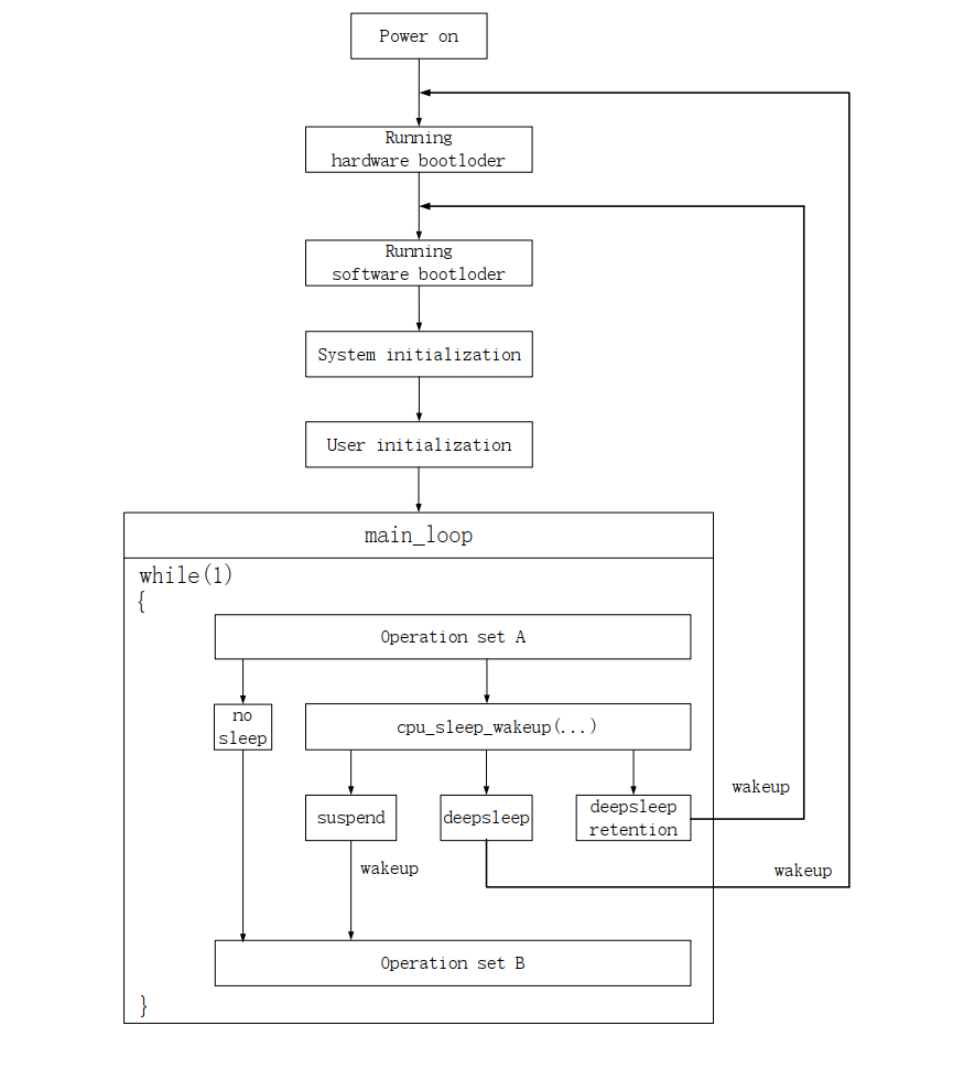
After the MCU is powered on, processes are as follows:
(1) Run hardware bootloader
The MCU hardware performs a set of fixed operations that are hardwired and cannot be modified by software.
A few examples are provided to illustrate these operations, for example: chip power on/deep back: determine the firmware memory address (offset address 0x00000/0x20000/0x40000/0x80000) that should be running by reading the boot flag "TLNK" of the flash. Then jump to the corresponding address of flash (base address 0x20000000 + offset address 0x00000/0x20000/0x40000/0x80000) to start executing the software bootloader.
(2) Run software bootloader
After the hardware bootloader has finished running, the MCU starts running the software bootloader. The software bootloader is the vector side (corresponding to the assembler program inside cstartup_B91.S), as described earlier.
The software bootloader is used to set up the memory environment for the C program to run later, which can be understood as the initialization of the whole memory.
(3) System initialization
System initialisation corresponds to the initialization of each hardware module (including sys_init, rf_drv_init, gpio_init, clock_init) from sys_init to user_init in the main function, and sets the state of digital/analog registers of each hardware module.
(4) User initialization
User initialisation corresponds to the function user_init in the SDK.
(5) main_loop
After User initialization is complete, enter main_loop controlled by while(1). The series of operations before entering sleep mode in main_loop is called "Operation Set A", and the series of operations after waking up from sleep mode is called "Operation Set B".
If the cpu_sleep_wakeup function is called to enter deepsleep mode, when deepsleep is woken up, the MCU will revert to Run hardware bootloader.
It can be seen that deepsleep wake_up shares almost the same process as Power on, and all the hardware and software initialization have to be redone again.
After the MCU enters deepsleep, all Sram and digital/analog registers (with the exception of a few analog registers) are powered down, so power consumption is very low and MCU current is less than 1µA.
Low Battery Detection
The expression "low battery detect" is used consistently throughout this document.
The Importance of Low Battery Detection
As battery gradually declines, when the voltage reaches a certain value, battery-powered products can have many problems:
(1) The B91 operating voltage ranges from 1.8V to 4.3V. When the voltage falls below 1.8V, stable operation can not be guaranteed.
(2) When the battery voltage is low, due to the unstable power supply, the "write" and "erase" operations of the flash may be at risk of errors, resulting in abnormal modification of program firmware and user data, and ultimately causing the product failure. Based on previous mass production experience, the low voltage threshold for this possible risk is set at 2.0V.
Based on above description, products powered by batteries must be set to a secure voltage, and the MCU is allowed to continue operation only when the voltage is higher than this secure voltage. Once the voltage falls below the secure voltage, the MCU stops running and needs to be shutdown immediately (this is done by entering deepsleep mode on the SDK).
The safety voltage (also termed alarm voltage) is currently set to 2.2V by default in the SDK. If user has a suboptimal harware design that leads to deterioration in the stability of the power supply network, the secure voltage value needs to be further increased, such as 2.3V, 2.4V, etc.
For product beyond development phase, as long as it is powered by battery, low battery detection must be a real-time task throughout the life cycle of the product, in order to ensure the stability of the product.
Realization of Low Battery Detection
Low battery detection requires the use of an ADC to measure the supply voltage. Please refer to the relevant ADC chapter in the Driver SDK Developer Handbook to get knowledge of the ADC module first.
The realization of the low battery detection is illustrated with the realization given in the SDK project example "proj_live_mic_tx", refer to the files bat.c and bat.h.
Make sure that the macro "ENABLE_BATT_CHECK" is turned on in the app_config.h file. This macro is turned off by default, so take care when using the low battery detection function.
#define ENABLE_BATT_CHECK 1
Considerations for Low Battery Detection
Low battery detection is a basic ADC sampling task, and there are some issues to be aware of when using an ADC to sample the supply voltage, as explained below.
Recommended GPIO Input Channel
Sampling can be done by Vbat or GPIO analog signal input, but the sampling accuracy of the Vbat channel is lower, and it is recommended to sample by external GPIO for occasions requiring high sampling accuracy.
The available GPIO input channels are the input channels corresponding to PB0~PB7, PD0 and PD1.
typedef enum{
    ADC_GPIO_PB0 = GPIO_PB0 | (0x1<<12),
    ADC_GPIO_PB1 = GPIO_PB1 | (0x2<<12),
    ADC_GPIO_PB2 = GPIO_PB2 | (0x3<<12),
    ADC_GPIO_PB3 = GPIO_PB3 | (0x4<<12),
    ADC_GPIO_PB4 = GPIO_PB4 | (0x5<<12),
    ADC_GPIO_PB5 = GPIO_PB5 | (0x6<<12),
    ADC_GPIO_PB6 = GPIO_PB6 | (0x7<<12),
    ADC_GPIO_PB7 = GPIO_PB7 | (0x8<<12),
    ADC_GPIO_PD0 = GPIO_PD0 | (0x9<<12),
    ADC_GPIO_PD1 = GPIO_PD1 | (0xa<<12),
}adc_input_pin_def_e;
Use of GPIO input channel for power voltage ADC sampling is as follows: directly connect the power supply to the GPIO input channel in the hardware circuit design. When initializing ADC, set GPIO to a high resistance state (ie, oe, output all set to 0), at this time, the voltage on the GPIO is equal to the power voltage, and ADC sampling can be done directly.
When initialisation, leave all states (ie, oe, output) to default without any special changes, the project example selects PB3 as the GPIO input channel by default.
Differential Mode Only
Although the ADC input mode supports both Single Ended Mode and Differential Mode, for some specific reasons, Telink specifies that only Differential Mode can be used and Single Ended Mode is not allowed.
The input channels of Differential mode is divided into positive input channel and negative input channel, and the measured voltage is the voltage difference between the positive input channel voltage and the negative input channel voltage.
If the ADC samples only one input channel, when using Differential mode, set the current input channel as positive input channel and GND as negative input channel, so that the voltage difference between the two is equal to the positive input channel voltage.
The SDK uses Differential mode for low voltage detection with the following function interface.
adc_set_diff_input(pin >> 12, GND);
ADC Tasks Switching Requirement
Low-voltage detection, as one of the most basic ADC sampling, uses the Misc channel. Users with ADC tasks other than low-voltage detection also need to use the Misc channel. Low-voltage detection cannot be run at the same time as other ADC tasks, and switching must be used to achieve such tasks.
Use of Low Battery Detection
In the SDK project examples, both proj_live_mic and proj_live_mic_240 have realized the low battery detection function, and user needs to turn on the low battery detection function in app_ui.h for use.
Low Battery Detection Initialisation
The default initialisation in the SDK is:
bat_check_init(ADC_GPIO_PB3, 0, 1, 2200, 2300);
The first parameter pin: set the pin for low battery detection, SDK defaults to PB3.
The second parameter res_up and the third parameter res_down: power detection voltage division factor. Because the low battery detection is based on GPIO, when the detection value is more than 3.5V, the value will start to deviate, so if the detection voltage is more than 3.5V, user needs to configure the voltage division factor manually. The SDK defaults to no voltage division, i.e., the value of res_up is 0 and res_down is 1. The specific calculation address is in the bat_get_voltage_mv interface in the bat.c file:
int bat_get_voltage_mv(void)
{
    ......
    adc_buf[adc_buf_index++] = vol *
            (bat_check_info.res_up + bat_check_info.res_down) / bat_check_info.res_down;
    ......
}
The fourth parameter bat_low_mv: safe voltage, SDK defaults to 2200mv.
The fifth parameter bat_nor_mv: normal voltage, SDK defaults to 2300mv. From bat_low_mv and bat_nor_mv is the transition phase, which is to prevent frequent switching between low battery and normal state.
Also the bat_check_info variable is a low battery detection structure.
typedef struct {
    adc_input_pin_def_e pin;
    int res_up;
    int res_down;
    int bat_low_mv;
    int bat_nor_mv;

    u32 tick_debounce;
    u32 debounce_time;

    u32 tick_check;
    u32 check_interval;

    int bat_state_curr;
    int bat_state_last;

    int bat_low;
    int bat_vol_mv;
} bat_check_info_s;
The first five variables are low battery detection initialisation in-parameters.
The sixth variable tick_debounce: low battery state switching timer, default is 1000 in microseconds, used to switch low battery state periodically.
The seventh variable debounce_time: low battery state switching timing, default is 1000 in microseconds.
The eighth variable tick_check: bat_check_task task execution timer for periodic execution of the low battery detection.
The ninth variable check_interval: bat_check_task task execution timing, default is 1000 in microseconds.
The tenth variable bat_state_curr: current low battery state.
The eleventh variable bat_state_last: last low battery state. Determined by comparing with the current low battery state, if the current low battery state is not consistent with the last one, start updating the low battery state parameter.
The twelfth variable bat_low: low battery state parameter, 0 is non-low battery state, 1 is low battery state, user can judge whether it is low battery state by getting the state of this variable.
The thirteenth variable bat_vol_mv: current power in mv.
Low Battery Detection Processing
Low battery detection processing can be achieved by calling bat_check_task() in ui_loop.
The variable tick_check is used to control the frequency of the low power detection execution, which in the project example is every 20ms. The developer can modify this value according to needs. When the operating voltage changes from more than 2300mv to less than 2200mv, the value of bat_state_last is 0 and bat_state_curr becomes 1. The current battery level is not the same as the last one, so it starts to update the low battery state variable, and assigns the bat_state_curr value of 1 to bat_low, thus realizing the switching of the low battery state.
USB Port
USB Audio Related Macro Description
APP_MODE: Set the USB function, the following three setting items are supported:
(1) APP_MODE_DEBUG_ONLY: Supports USB Log, VCD, and command input;
(2) APP_MODE_DEBUG_HID:Supports USB Log, VCD, command input, and HID communication;
(3) APP_MODE_AUDIO_AUTO: Supports USB Speaker, USB MIC, HID communication.
When APP_MODE == APP_MODE_AUDIO_AUTO, the USB Audio function is enabled, and the following macros can be set:
(a) USB_SPEAKER_ENABLE enables USB Speaker (USB Downstream) (b) USB_MIC_ENABLE enables USB MIC (USB Upstream) (c) USB_MIC_CHANNEL: 1: USB MIC/upstream in mono; 2: USB MIC/upstream in stereo
Among them, USB Speaker and USB MIC can be turned on independently or at the same time; USB Speaker only supports stereo.
USB Audio Descriptor Name Initialisation
The USB Audio descriptor name initialisation configuration is in the app_config.h file:
......
#define STRING_PRODUCT                     L"Live MIC"
#else
#define STRING_PRODUCT                     L"USB Speaker"
#endif
......
The default value is in the default_config.h file, it is recommended to change it in app_config.h.
......
#ifndef STRING_VENDOR
#define STRING_VENDOR       L"Telink"
#endif
#ifndef STRING_PRODUCT
#define STRING_PRODUCT      L"2.4G Wireless Audio"
#endif
#if (MCU_CORE_TYPE == MCU_CORE_9518)
    #ifndef STRING_SERIAL
    #define STRING_SERIAL       L"TLSR9518"
    #endif
#else
    #ifndef STRING_SERIAL
    #define STRING_SERIAL       L"TLSR9518"
    #endif
#endif
......
Algorithms
SDK supports multiple algorithms.
Where the audio stream on the TX side is as follows:
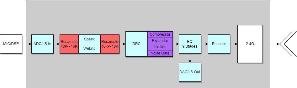
The audio stream on the RX side is as follows:
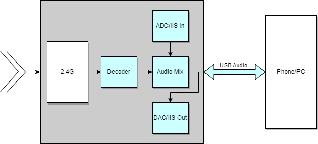
Resampling Algorithm
Resampling Algorithm Initialisation
Calling "my_resample48to16_init" and "my_resample16to48_init" in the app_audio_init interface of the app_audio.c file corresponds to downsampling (48k-16k) and upsampling (16k-48k) initialisation, respectively.
void app_audio_init (void)
{
    ......
    #if RESAMPLE_48_TO_16_EN
    my_resample48to16_init();
    #endif

    #if RESAMPLE_16_TO_48_EN
    my_resample16to48_init();
    #endif
    .....
}
Resampling Algorithm Processing
The current resampling algorithm processing is mainly applicable to sampling rate adjustment in noise reduction algorithm processing project.
(1) In default noise reduction mode:
Downsampling before noise reduction and upsampling after noise reduction on Tx side;
On the Rx side, there is no resampling processing.
(2) In long distance noise reduction mode:
Downsampling before noise reduction on the Tx side, then encoding;
Upsampling first after decoding on the Rx side.
EQ
EQ is enabled by enabling the APP_EQ_ENABLE macro.
EQ Initialisation
#if(APP_BUILD == APP_MIC_TX) && APP_EQ_ENABLE
    eq_inf_load(0x20000000 + Flash_USER_EQ_BASE);
    myudb_register_hci_eq_cb(my_debug_eq);
    audio_codec_flag_set(CODEC_FLAG_EQ_VOICE_MIC_EN, 1);
#endif
eq_inf_load(0x20000000 + Flash_USER_EQ_BASE): Used to read eq data, if no eq data is stored at this address, the default eq parameter in the eq.c file is used:
float32_t coeff_eq_voice_mic_left[5 * NSTAGE_EQ_VOICE_MIC_MAX]={
    0.983146317605274,-1.896277815330497,0.925516368712182,1.896277815330497,-0.908662686317456,//800Hz

    1.018304336102112,-1.823726756975888,0.907922907437080,1.823726756975888,-0.926227243539192,//2300Hz

    1.382406919700922,-0.529089646178078,0.000170953890723,0.529089646178078,-0.382577873591645,//3000Hz

    1.018304336102112,-1.823726756975888,0.907922907437080,1.823726756975888,-0.926227243539192,//2300Hz
};
myudb_register_hci_eq_cb(my_debug_eq): Used to register the EQ online debugging interface.
audio_codec_flag_set(CODEC_FLAG_EQ_VOICE_MIC_EN, 1): used to enable EQ of codec.
EQ Processing
Perform EQ processing in the app_audio_task interface:
_attribute_ram_code_ void app_audio_task ()
{
    ......
#if APP_EQ_ENABLE
    if (audio_codec_flag_get(CODEC_FLAG_EQ_VOICE_MIC_EN))
    {
        g_eq_para.eq_type        = EQ_TYPE_VOICE_MIC;
        g_eq_para.eq_sample_rate = EQ_SAMPLE_RATE_48K;

        g_eq_para.eq_channel = EQ_CHANNEL_LEFT;
        g_eq_para.eq_nstage = instance_eq_voice_mic_left.nstage;
        eq_proc(g_eq_para, pcm, pcm, samples, 0);
    }
#endif
    ......
}
EQ processing is performed by executing the eq_proc function.
EQ Tool
EQ Tool is a tool used by Telink for debugging EQ, the EQ Tool is described below:
First open the Telink BDT tool, click on Tool and in the drop down menu, select TWS Tool.
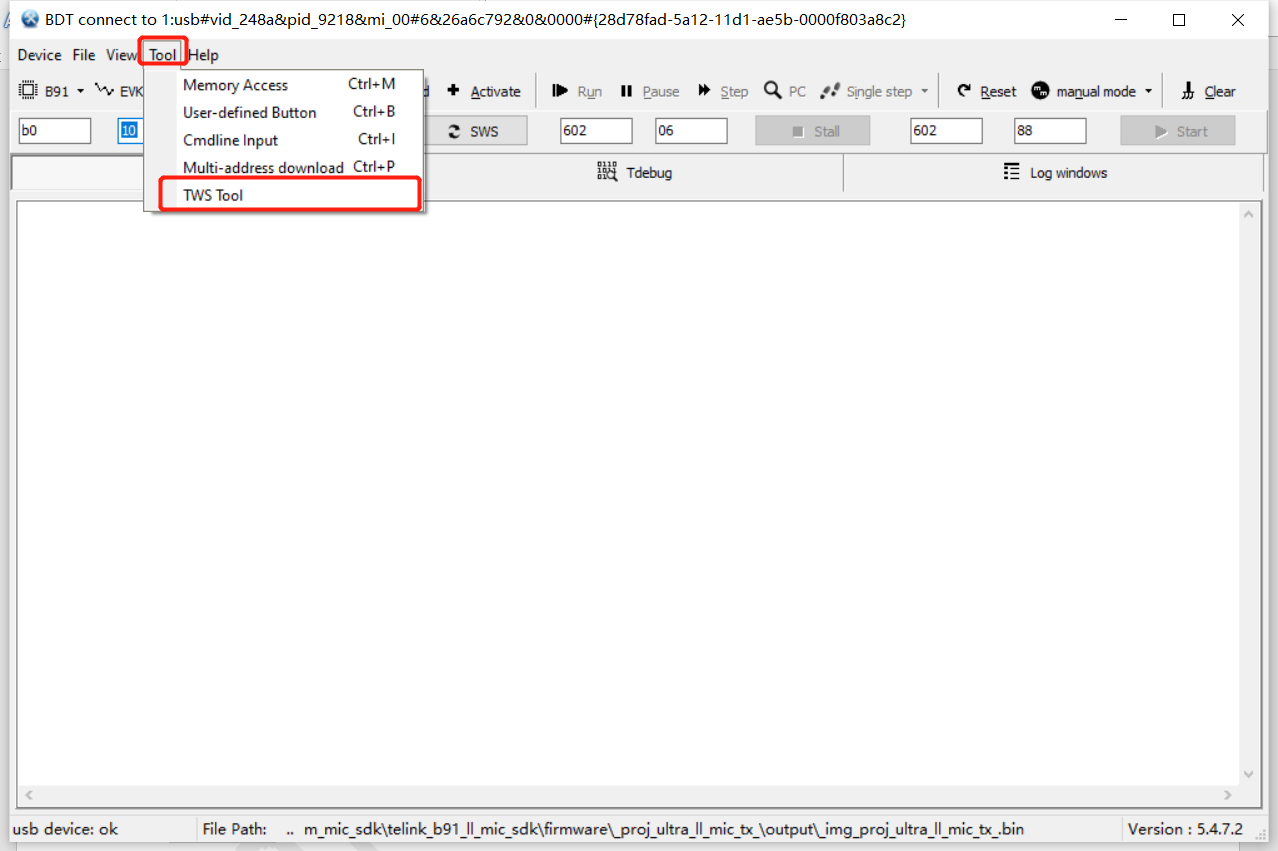
Select EQ Tool, which is divided into 5 main areas, which are:
(1) Visualisation area: Used to visualise the EQ parameters for debugging purpose.
(2) Configuration area: Used to configure the EQ initialisation configuration. Among them,
(a) FreqSmp:Sample rate, the SDK defaults to 48k; (b) Channel:Left and right as well as stereo are supported, the SDK defaults to left channel; (c) Stages:The number of frequency points, the default supports 4 frequency points; (d) Mode:EQ mode, the SDK defaults to Speech Mic; (e) Gain:Decrease the gain of all frequency points in the range of -10 ~ 0.
(3) Debug area: For debugging EQ parameters. Among them,
(a) Type:Filter Type; (b) Q:Slope; (c) Fc(Hz):Frequency point; (d) dB:Gain.
(4) Operation area: Used to update EQ parameters online, save EQ parameter bin files, and generate EQ parameter codes.
(5) Parameter generation area: Used to display log and to generate EQ parameters.
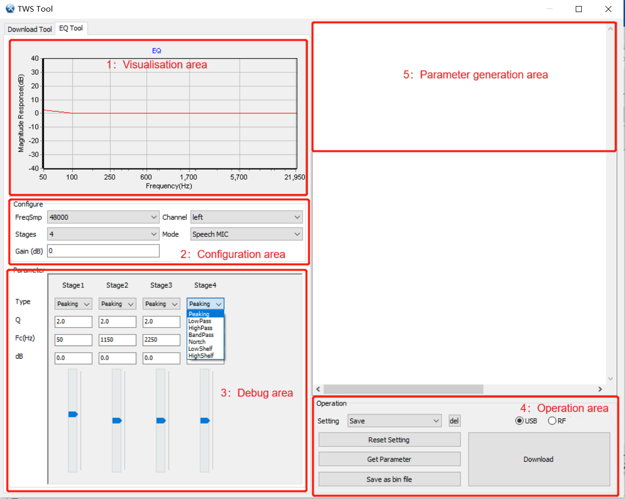
Next are illustrations how to update EQ parameters:
(1) USB online update: configure APP_MODE macro as APP_MODE_DEBUG_ONLY or APP_MODE_DEBUG_HID, make sure that the device and PC can print the log, select USB in the operation area, click Download, and the log of the parameter update can be seen in the risc-v TDB tool.
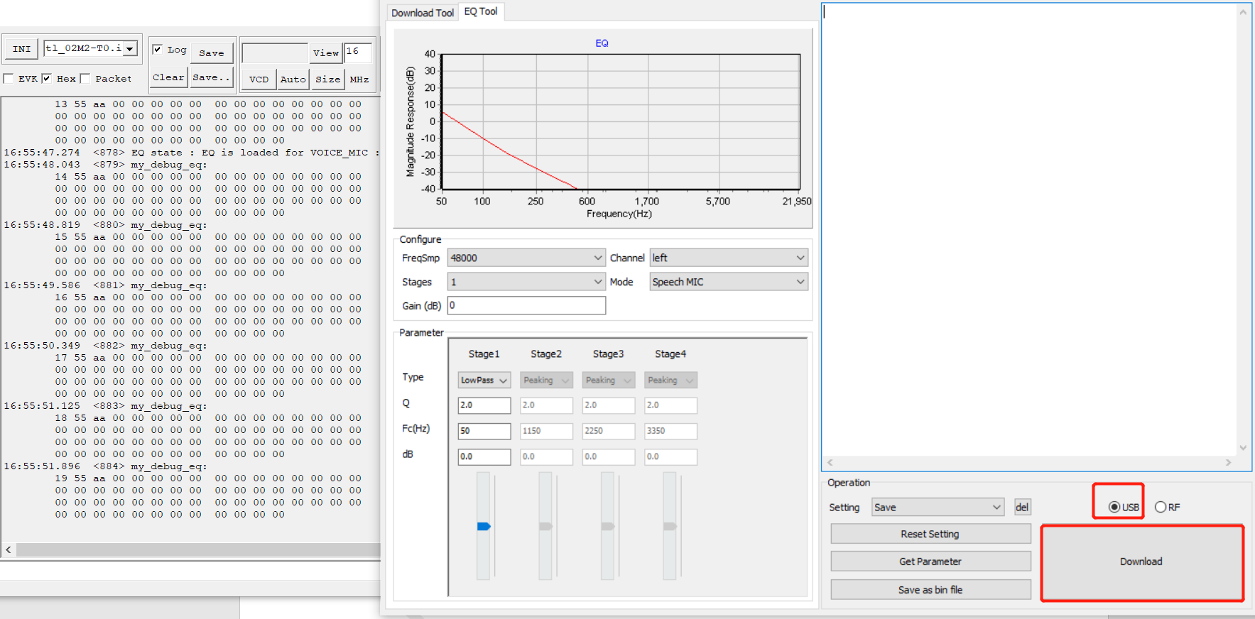
(2) Generate Parameter Update: Click Get Parameter to generate the corresponding EQ parameter code in the Parameter Generation area, replace this code with the default eq parameter code location mentioned above.
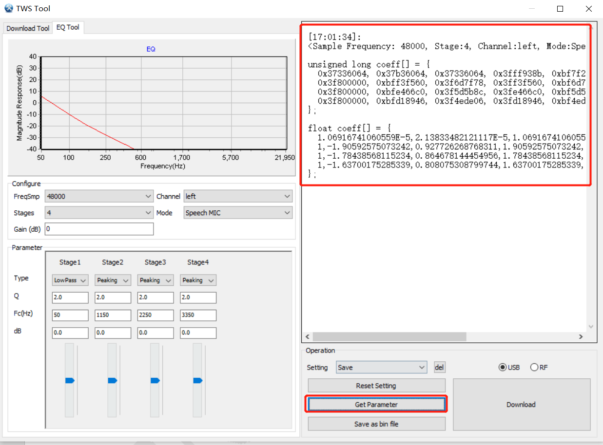
(3) Generate file update: Click Save as bin file to generate a bin file of eq in the specified path, then use Telink TDB's Download Tool to burn the bin file to the address of 0xDC000.
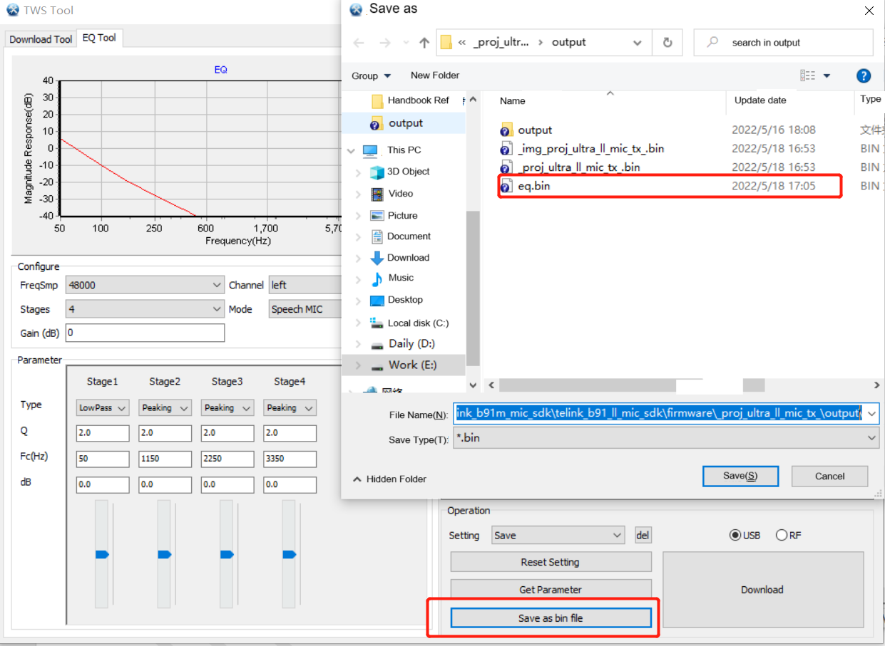
Noise Reduction Algorithm
The APP_NS_ENABLE macro enables noise reduction.
If the APP_WB_NS_ENABLE macro is enabled, use the webrtc algorithm (better performance); otherwise, use the Speex algorithm.
The APP_NS_MODE macro selects the noise reduction mode:
FS_16K_NS_EN, default noise reduction mode, processing - Tx side resamples 1 frame 48K data to 16K -> NS -> resample to 48K again, encode, send N times, Rx side receives packets N times, decode, play.

LD_16K_NS_EN, long distance noise reduction mode, processing - Tx side resamples 3frame 48K data to 16k -> NS encode, send 3N times, Rx side receives packets 3N times, decode, resample to 48K, play.
Note
- Long-distance noise reduction mode only supports LC3+ coding, SBC coding is not supported.
Noise Reduction Algorithm Initialisation
Initialisation in the void app_audio_init() interface
void app_audio_init ()
{
    ......
    #if APP_WB_NS_ENABLE
        app_w_ns_init();
    #else
        app_ns_init();
    #endif
    ......
}
(1) Speex algorithm
void app_ns_init(void)
{
    nsParas.noise_suppress_default = -15;
    nsParas.echo_suppress_default = -55;
    nsParas.echo_suppress_active_default = -45;
    nsParas.low_shelf_enable = 1;
    nsParas.ns_smoothness = 27853;      // QCONST16(0.85f,15)
    nsParas.ns_threshold_low = 100000.0f;

#if 0
    int nsSize = ns_get_size();
    my_dump_str_data(1, "NS Buffer Size", &nsSize, 4);   // 0x234E
    den = (SpeexPreprocessState*)malloc(nsSize);
#else
    static u32 ns_buffer[0x234E/4+256];
    den = (SpeexPreprocessState*)ns_buffer;
#endif
    ns_init(den, &nsParas, 16000 * MIC_SAMPLES_PER_PACKET / MIC_SAMPLING_RATE, SPEEX_SAMPLERATE);
}
noise_suppress_default: Adjusts the amplitude of noise attenuation in db, -15 means attenuation of 15 dB.
low_shelf_enable: When enabled, the low-frequency attenuation filter significantly attenuates signals below 100 Hz, concurrently reducing overall signal energy.
Note
- Other parameters are recommended to be left unchanged.
Where the input frame_size of the ns_init interface supports a maximum of 120.
(2) Webrtc algorithm
void app_w_ns_init(void)
{
    w_ns_cfg_param.frame_size = W_NS_FRAME_SIZE;
    w_ns_cfg_param.sampleRate = 16000;
    w_ns_cfg_param.target_level = k12dB;
    w_ns_cfg_param.lowShelf_En = 0;
    //int s = w_ns_get_size();
    //my_dump_str_data(1, "buffer size: %d\n", &s,4);

    w_ns_init(ns_buffer_st, w_ns_cfg_param);
}
Where the input parameter W_NS_FRAME_SIZE of the app_w_ns_initns_in interface supports a maximum of 80, and packet grouping is performed if the frame length exceeds 80.
Noise Reduction Algorithm Processing
In addition to the differences between the webrtc algorithm and the speex algorithm, the most important thing to focus on during the noise reduction process is the difference between the noise reduction modes.
(1) Default noise reduction mode
Tx side processing:
_attribute_ram_code_ void app_audio_task (void)
{
    ......
    #if APP_NS_MODE == FS_16K_NS_EN
        if (async.aec_enable) {
            s16 pcm16k[samples/3];
            my_resample48to16_data((int *)pcm, samples, (int *)pcm16k, 0);
            log_task (SL_AUDIO_EN, SL01_task_tws_arbiter_en, 1);
            app_ns_process_frame(pcm16k, samples/3);
            log_task (SL_AUDIO_EN, SL01_task_tws_arbiter_en, 0);
            my_resample16to48_data((int *)pcm16k, samples/3, (int *)pcm, 0);
        }
    ......
        ps->cmd = ASYNC_CMD_AUDIO_TAG;
        #if CODEC_ALGORITHM_SEL == CODEC_ALGORITHM_SBC
            mic_audio_encode(pcm, samples, enc);
            tmemcpy (ps->data, enc, ASYNC_AUDIO_DATA_LEN);
        #elif CODEC_ALGORITHM_SEL == CODEC_ALGORITHM_LC3A
            __UNUSED int leni = my_llenc (0, pcm, samples, enc);
            tmemcpy (ps->data, enc, ASYNC_AUDIO_DATA_LEN);
        #endif
    #endif
    ......
}
Line 7: Resample 1 frame 48K data to 16K.
Line 9: NS.
Line 11: Resample to 48K again.
Line 14 ~ 21: SBC/LC3+ encoding, send N times.
Processing on Rx side: Receive packet N times, decode, play.
DRC Algorithm
DynAMIC Range Control (DRC) provides compression and amplification functions to make sounds softer or louder, i.e., a way of signal amplitude adjustment. DRC is widely used in audio signal processing, such as Wide DynAMIC Range Compression (WDRC), the most common method in hearing aids; Automatic Gain Control (AGC), the most common method in audio signal processing and so on. DynAMIC range control, as the name suggests, maps the dynamic range of the input audio signal to a specified dynamic range. Usually the dynamic range after mapping is smaller than the dynamic range before mapping, so it is called dynamic range compression. The audio signal can be subjected to overall dynamic range control; it can also be divided into a number of subbands for separate dynamic range control. The specific principle can be referred to: DRC Principles
The DRC in SDK is divided into ADC DRC and DAC DRC, which are controlled by ADC_DRC_EN and DAC_DRC_EN macros respectively.
The following is an example of an ADC DRC.
DRC Initialisation
The DRC algorithm is enabled by enabling the ADC_DRC_EN macro.
void app_drc_init(drc_nodes_s *drc_nodes, u32 Flash_addr)
{
    app_Flash_read(Flash_addr, sizeof(drc_paras_set_num), (u8 *)&drc_paras_set_num);
    if (drc_paras_set_num > 0 && drc_paras_set_num <= DRC_NODE_MAX) {
        u32 addr = Flash_DRC_PARA_BASE + sizeof(drc_paras_set_num);
        app_Flash_read(addr, drc_paras_set_num * sizeof(drc_node_para_s), (u8 *)drc_paras_set);
        drc_nodes_init_paras(drc_nodes, drc_paras_set, drc_paras_set_num);
        drc_paras_set_num = 0;
    }
    else{
        #if DAC_DRC_EN
            drc_nodes_init_paras(drc_nodes, dac_drc_node_paras_default, ARRAY_LEN(dac_drc_node_paras_default));
        #elif  ADC_DRC_EN
            drc_nodes_init_paras(drc_nodes, adc_drc_node_paras_default, ARRAY_LEN(adc_drc_node_paras_default));
        #endif
    }
    drc_nodes_update(drc_nodes);
}
The parameters for initialising the DRC algorithm are preferentially read from the flash address, if the DRC parameters are not stored to the specified address, the default DRC parameters are used for initialisation.
drc_node_para_s adc_drc_node_paras_default[] =
{
    {
        .type = DRC_NOISE_GATE,
        .noise_gate = {
                -50.0f, 4.0f, 0.05f, 0.1f, 0.05f, MIC_SAMPLING_RATE, VALUE_0dBFS, 1
        },
    },
    {
        .type = DRC_EXPANDER,
        .expander = {
                -70.0f, (float)20, (float)4, 0.01f, 0.05f, 0.000f, (float)MIC_SAMPLING_RATE, 0, VALUE_0dBFS, 48*2
        },
    },
    {
        .type = DRC_COMPRESSOR,
        .compressor = {
                -6.0f, 3.0f, 4.0f, 0.05f, 1.0f, MIC_SAMPLING_RATE, 0, VALUE_0dBFS, 48
        },
    },
    {
        .type = DRC_LIMITER,
        .limiter = {
                -3.0f, 1.0f,  0.01f, 0.1f, MIC_SAMPLING_RATE, 0, VALUE_0dBFS, 48
        },
    },
};
DRC Processing
Call drc_process_frame interface for DRC processing.
static inline PCM_MONO_INT drc_gain_process_single_point(PCM_MONO_INT pcm, float gain)
{
    float v = (float)pcm * gain;
    for(int j=0; j<__drc_nodes->drc_cnt; j++) {
        v = drc_calc_output(&__drc_nodes->drc[j], v);
    }
    v += 0.5f;
    return SATURATE_PCM(v);
}
_attribute_ram_code_ int drc_gain_process_frame(drc_nodes_s *drc_nodes, PCM_MONO_INT *pcm, int len, float gain)
{
    __drc_nodes = drc_nodes;
    for(int i=0;i<len;i++) {
        pcm[i] = drc_gain_process_single_point(pcm[i], gain);
    }
    return len;
}
DRC Tool
The DRC tool is used to debug the DRC and generate the corresponding parameter code with the following interface:
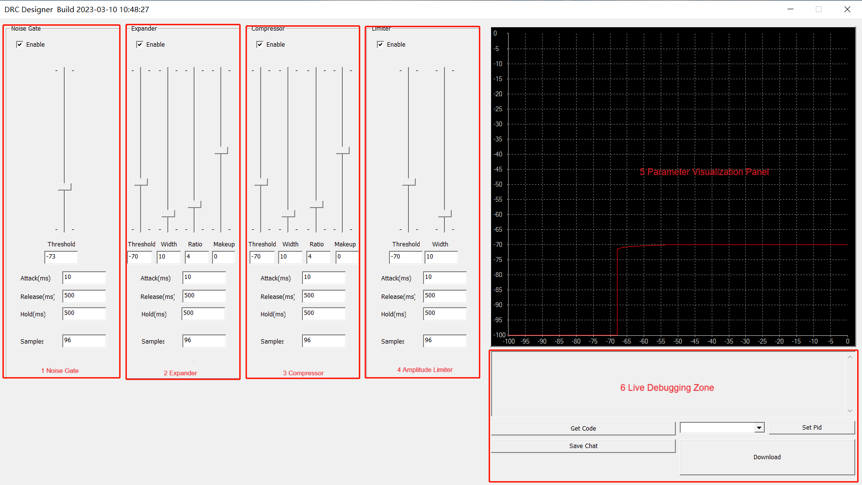
(1) Noise gate: A type of expander that limits signals below a given threshold.
(a) Threshold: Door closing dB; (b) Attack:Closing to opening time; (c) Release:Opening to closing time; (d) Hold:Door opening status hold time; (e) Samples:Calculate points, calculate per 96 points by default.
(2) Dynamic range expander: Attenuates the volume of small signals below a given threshold; make small signals sound even smaller.
(a) Threshold:Expansion dB; (b) Width:Degree of excessive smoothing of inflection points for smoothing processing; (c) Ratio:Slope; (d) Makeup:Gain; (e) Others as above.
(3) Dynamic range compressor (DRC): Attenuates the volume of loud signals that exceeds a given threshold; protects the hardware and increases the overall loudness.
(4) DynAMIC range limiter: A type of compressor that limits the signal above a given threshold.
After setting the DRC parameters, click Get Code.
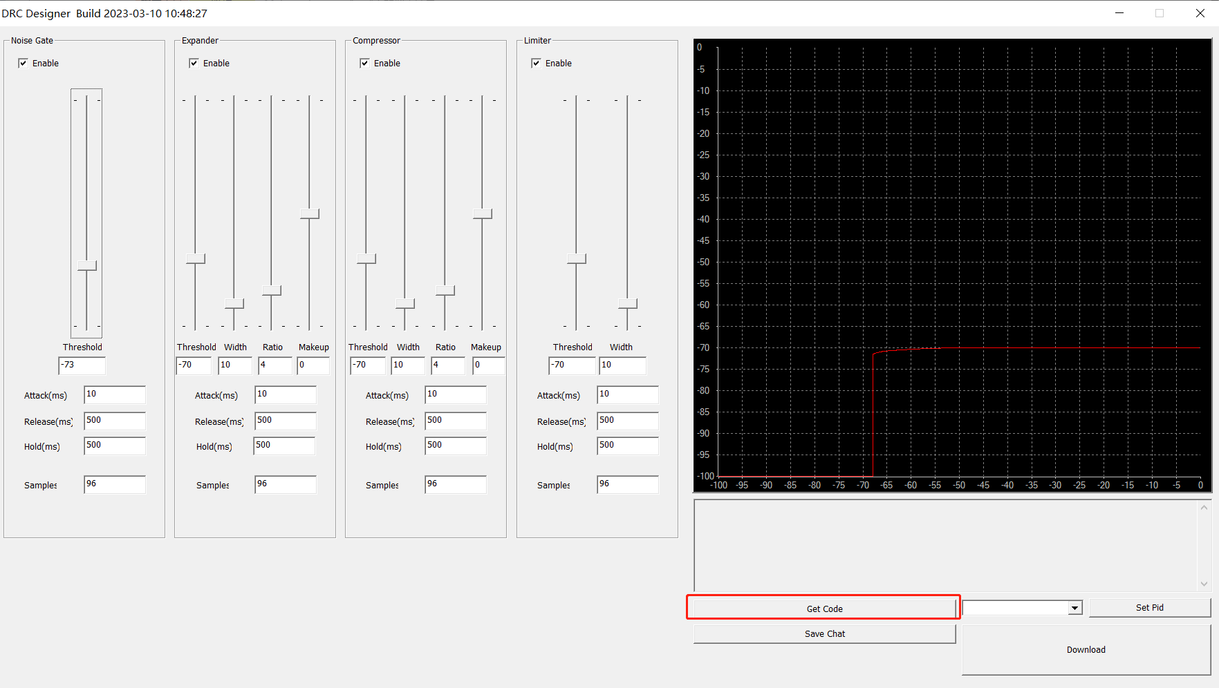
The DRC parameter code as shown in the figure is then generated:
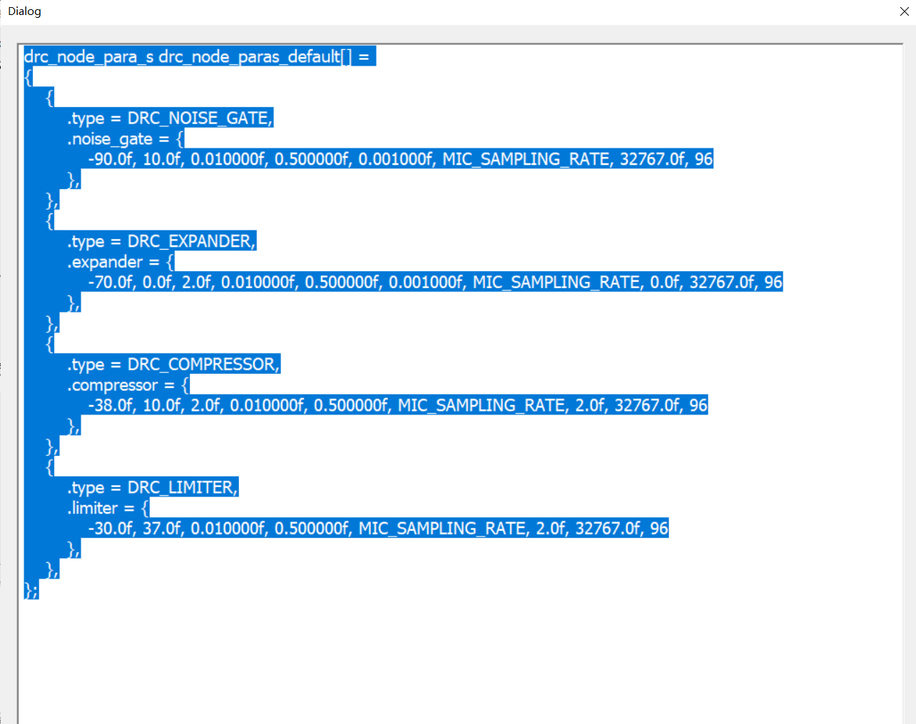
DRC parameters can be imported by replacing the default DRC parameter variable with this parameter.
Or enable CFG_COMMUNICATION_BY_USB macro and configure APP_MODE to APP_MODE_DEBUG_HID or APP_MODE_AUDIO_AUTO to enable online debugging. (APP_MODE_DEBUG_HID mode is used here for easy log checking)
When "USB Connected" is printed, indicating a successful connection.
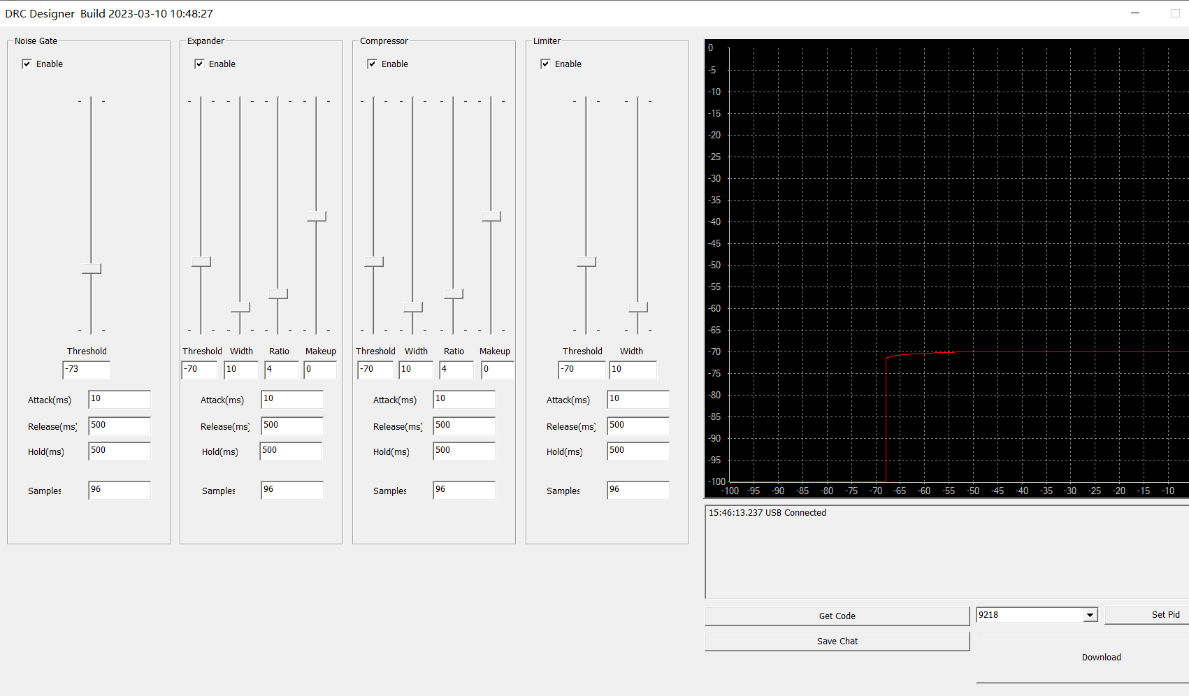
Then tick the required parameters and click Download to download the parameters.
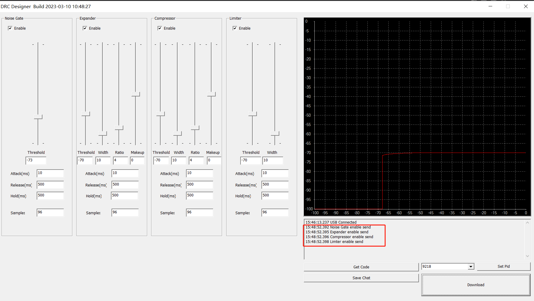
Finally, the DRC online debugging parameters sent by the host computer can be viewed in the lower log.
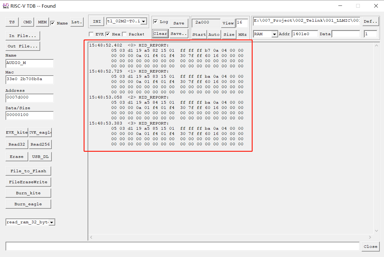
Note
- DRC online debugging performs a parameter comparison, and if the parameters sent are the same as those currently employed, they will not be processed.
Audio
Audio Initialisation
TX Audio Initialisation
The Audio input source on the Tx side can be I2S, lineIn, DMIC, and AMIC. Local Lineout monitoring of the input audio is supported and can be switched off, controlled via the CODEC_DAC_MONO_MODE macro.
(1) LineIn/AMIC: The default audio input path on the development board, where LineIn requires shorting jumper pins 34 and 33.
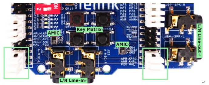
To switch to the analog microphone path, relocate the jumper from PIN 34/33 to PIN 30/29 (Left_Mic enabled by default).
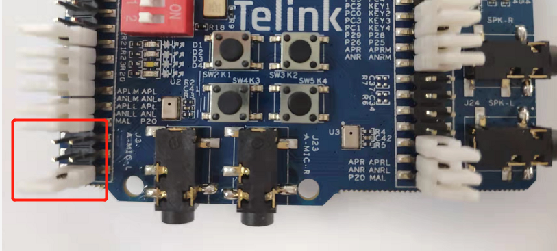
(2) DMIC: Uses a dedicated audio processing chip to read digital signals directly into R9, requiring the "AUDIO_IN_MODE" macro to be set to "DMIC_INPUT".
void app_audio_init ()
{
    ......
#ifdef AUDIO_IN_MODE
    if (AUDIO_IN_MODE == DMIC_INPUT) {
    #ifdef DMIC_GPIO_SEL
        audio_set_dmic_input(DMIC_GPIO_SEL);
    #endif
    }
    else {
        audio_set_input_mode(AUDIO_IN_MODE);
    }
#endif
    ......
}
(3) I2S: Host computer by default, need to set "AUDIO_INTERFACE" macro to "AUDIO_I2S_GPIO".
void app_audio_init ()
{
    ......
#if(AUDIO_INTERFACE == AUDIO_I2S_GPIO)
    audio_set_interface(FLAG_INTERFACE_GPIO, 1);
    #if (AUDIO_INTERFACE_ROLE == AUDIO_I2S_AS_SLAVE)
        gpio_input_en(I2S_BCK_PC3|I2S_DAC_LR_PC6|I2S_DAC_DAT_PC7);
        audio_set_interface(FLAG_INTERFACE_ROLE_SLAVE, 1);
    #else
        audio_set_interface(FLAG_INTERFACE_ROLE_SLAVE, 0);
    #endif
#else
    ......
}
The I2S initialisation pins are PC3 (BCK), PC6 (LR) and PC7 (DAT_IN).
RX Audio Initialisation
(1) Lineout: Default audio output. If USB Audio is turned on, it adds USB MIC upstream, and supports USB Audio downstream for mixing with the remote Tx audio output from Lineout.
(2) I2S:Selectable audio output, set the AUDIO_INTERFACE macro to AUDIO_I2S_GPIO, initialisation pins are: PC3 (BCK), PC4 (LR), PC5 (DAT_OUT). If USB Audio is turned on, it adds USB MIC upstream, and also supports USB Audio downstream for mixing with the remote Tx audio from the I2S output.
Gain Initialisation
(1) Tx side: Adjust the input gain of AMIC and DMIC as well as Lineout gain, which are controlled by CODEC_IN_A_GAIN (0 ~ 20dB), CODEC_IN_D_GAIN (0 ~ 43dB), and CODEC_OUT_A_GAIN (-19 ~ 12dB) and CODEC_OUT_D_GAIN (-31 ~ 32dB) respectively.
(2) Rx side: Only Lineout gain is valid, controlled by CODEC_OUT_A_GAIN, CODEC_OUT_D_GAIN, initialisation interface as above.
void app_audio_init ()
{
    audio_set_codec_in_path_a_d_gain(CODEC_IN_D_GAIN, CODEC_IN_A_GAIN);    //mic sco
    audio_set_codec_out_path_a_d_gain(CODEC_OUT_D_GAIN, CODEC_OUT_A_GAIN); //mic sco
    .......
}
The Tx / Rx gain can be configured directly through the app_ui.h file.
    #if APP_BUILD == APP_MIC_TX
        #define CODEC_IN_A_GAIN               CODEC_IN_A_GAIN_0_DB
        #define CODEC_IN_D_GAIN               CODEC_IN_D_GAIN_0_DB
        #define CODEC_OUT_A_GAIN              CODEC_OUT_A_GAIN_0_DB
        #define CODEC_OUT_D_GAIN              CODEC_OUT_D_GAIN_0_DB
    #elif APP_BUILD == APP_MIC_RX
        #define CODEC_IN_A_GAIN               CODEC_IN_A_GAIN_0_DB
        #define CODEC_IN_D_GAIN               CODEC_IN_D_GAIN_0_DB
        #define CODEC_OUT_A_GAIN              CODEC_OUT_A_GAIN_0_DB
        #define CODEC_OUT_D_GAIN              CODEC_OUT_D_GAIN_0_DB
    #endif