Telink Platform SDK Developer Handbook
Platform SDK Overview
SDK Introduction
Telink offers two sets of Platform SDKs, each corresponding to different chip architectures:
- tc_platform_sdk: Chip series with Telink's self-developed TC32 core
- tl_platform_sdk: Chip series with RISC-V architecture.
Both SDKs provide complete drivers, sample codes, and development tools to help you quickly build embedded applications based on Telink chips.
Based on core architecture, chips are divided into TC series and TL series. The table below summarizes the key features of all supported chips:
| series | SDK | Chip codename | The number of cores | Core | RAM | Cache | Mailbox channels |
|---|---|---|---|---|---|---|---|
| TC | tc_platform_sdk | B80 | 1 | TC32 | Single RAM | Cache in RAM | — |
| B80B | |||||||
| B85 | |||||||
| B87 | |||||||
| TC321x | |||||||
| TC122x | |||||||
| TC123x | |||||||
| TL | tl_platform_sdk | B91 | 1 | RISC-V D25F (with FPU) | IRAM+DRAM | I-Cache + D-Cache, Cache independent space |
— |
| B92 | 1 | RISC-V D25F (with FPU) | — | ||||
| TL321x | 1 | RISC-V D25F (Without FPU) | — | ||||
| TL322x | 2 | RISC-V D25F (with FPU) + N22 (without FPU) | D25F ↔ N22 | ||||
| TL323x | 1 | RISC-V D25F (with FPU) | — | ||||
| TL721x | 1 | RISC-V D25F (with FPU) | — | ||||
| TL751x | 3 | RISC-V D25F (with FPU) + N22 (without FPU) + DSP | D25F ↔ N22、D25F ↔ DSP、N22 ↔ DSP |
Note
- B91 includes TLSR951x and TLSR921x, B92 includes TLSR952x and TLSR922x, B80 / B80B includes TLSR8208 and TLSR8373, B85 includes TLSR825x and TLSR8359, B87 includes TLSR827x and TLSR8355.
- Multicore chips communicate via Mailbox; for details, see Mailbox.
SDK directory structure
tc_platform_sdk
tc_platform_sdk/
├── chip/                          # Chip-related code
│   └── <chip>/                    # For example, B80, B85, B87, TC321x
│       ├── boot/                  # Startup file
│       └── drivers/               # Driver code (including source code and precompiled static libraries in lib/)
├── common/                        # General code (basic types, strings, etc.)
├── demo/vendor/                   # Sample code
└── project/                       # Telink IoT Studio project files
    └── tlsr_tc32/
        └── <chip>/                # Chip projects, including .project/.cproject and boot.link
tl_platform_sdk
tl_platform_sdk/
├── chip/                          # Chip-related code
│   └── <chip>/                    # For example, B91, B92, TL321x
│       ├── boot/                  # Startup file
│       ├── drivers/               # Driver code (including source code and precompiled static libraries in `lib/`)
│       └── link/                  # Link scripts
├── common/                        # Cross-chip common code
├── demo/vendor/                   # Sample code
├── project/                       # Telink IoT Studio project files
│   └── tlsr_riscv/
│       └── <chip>/                # Chip engineering, including .project/.cproject
└── 3rd-party/                     # Third-party library
Directory Description
boot/: Startup file, responsible for power-on initialization: setting interrupt vector tables, initializing stack pointers, transporting data segments, and jumping to main function. TC and TL have different startup files; see Software Software Startup for detailsdrivers/: drivers, each peripheral module contains.hand.csource files; some modules (such as RF, PM) are provided as precompiled static libraries (.a) underlib/, with source code not disclosedlink/(TL): Link script that defines the program's memory layout, located atchip/<chip>/link/. The TC link script (boot.link) is located atproject/tlsr_tc32/<chip>/.See Software Startup for detailsproject/:Telink IoT Studio project file directory (Eclipse project.project/.cproject). TC is located atproject/tlsr_tc32/<chip>/,TL is atproject/tlsr_riscv/<chip>/demo/vendor/: sample code and reference designcommon/: Common code across different chips (such astypes.h,string.h,sdk_version.h, etc.)3rd-party/: Third-party open-source components (TL SDK only)reg_include/(TL): Register definition file (TL SDK only), containing register address mappings and bit-field definitions for each peripheral. The register definitions in the TC SDK are written directly into header files such asregister.h
SDK version
Both sets of SDKs embed version information at the end of the compiled firmware (the bin file), making it easy for tools or scripts to identify the SDK version used after burning.
Version format
The version is stored as a string with a $$$ delimiter, in the following format:
$$$<sdk_name>_<version>$$$
- TC series example:
$$$tc_platform_sdk_V3.4.0$$$ - TL series example:
$$$tl_platform_sdk_V3.9.0$$$
Implementation principle
The version number consists of three parts, with both SDKs implementing the same approach:
- Version macro definition (
common/sdk_version.h): Each chip model corresponds to an independent version macro (e.g.,B91_SDK_VERSION_NUM), whichSDK_VERSION_NUMuniformly references the version of the current compilation target. - Version array storage (
common/sdk_version.c): By combiningSDK_VERSION/SDK_VERSION1macros with C preprocessing#stringing operators, version macros are concatenated into complete delimiter strings, stored in thesdk_version[]array, and using__attribute__((section(".sdk_version")))to place it into a separate section named.sdk_version:
volatile __attribute__((section(".sdk_version"))) unsigned char sdk_version[] = {SDK_VERSION(SDK_VERSION_NUM)};
- Link script segment placement: The link script is kept via
KEEP(*(.sdk_version)) and placed at the end of the bin file, with the segment size included in theBIN_SIZE. TL SDK is located atchip/<chip>/link/*.link, TC SDK is atproject/tlsr_tc32/<chip>/boot.link.
Version identification
Since version information is fixed at the end of the bin file and wrapped by $$$ delimiters, it can be extracted directly from the binary file via script. The SDK provides tl_check_fw.sh scripts (../../tc_platform_sdk/tools/tl_check_fw_tool/tl_check_fw.sh) that use regular expression to match the $$$...$$$ pattern to extract and output the version. If the version information is not found at the end of the bin file, check whether sdk_version.c has been properly compiled and linked.
Boot ROM
Boot ROM Overview
The Boot ROM is the read-only boot code embedded inside the SoC and is the first program executed by the CPU after the device powers on and resets. It is the starting point of the entire system boot chain, responsible for the most basic hardware initialization and loading the next-stage bootloads.
The startup process of Telink chips is divided into two phases:
| Phase | Name | Description | Modifiable |
|---|---|---|---|
| Phase One | Boot ROM | The hardware boot logic is hardwired into the chip, and it cannot be modified | No |
| Phase Two | Software Startup | The SDK provides the startup files (cstartup. S + link file) | Yes |
Boot ROM, as the first phase, is executed first after powering on, resetting IO, or waking up from Deep Sleep (excluding deep retention). After completing the necessary initialization, it hands over control to the Software Startup in the second phase.
Boot ROM Features
Boot ROM has the following features:
- Read only, non-modifiable — hardwired in the chip's ROM, it cannot be erased, written, or modified by software after manufacturing, ensuring the integrity and security of the boot codes.
- Executes first after power-on — the first segment of codes executed after CPU reset. The hardware reset vector is fixed to the entry address of the Boot ROM; after the CPU powers on, the Boot ROM must be executed first
- Chip-level Root of Trust — Because it cannot be modified, the Boot ROM serves as the starting point of the trust chain for Secure Boot. In Secure Boot mode, the Boot ROM verifies the firmware image signature in the next phase. The boot process proceeds only after the signature verification succeeds.
ROM function modes
Boot Mode
The ROM supports two Boot Modes: Normal Boot and Secure Boot. Normal Boot is mandatory for all chip support; Secure Boot is optional and available on some chips, enabled through eFuse/OTP configuration. Once enabled, for security reasons, you cannot switch back to Normal Boot.
Normal Boot
Normal Boot is the default boot mode, executing the standard firmware startup process quickly and is suitable for general application scenarios.
Secure Boot
Secure Boot adds security-related features (configured to Secure Boot mode via eFuse or OTP):
- Before booting the firmware, the Boot ROM performs signature verification on the firmware
- Only firmware that passes signature verification will be executed
- If signature verification fails, the chip will refuse to start the firmware, preventing unauthorized or tampered codes from running Secure Boot provides end-to-end security protection starting from the hardware root of trust, suitable for applications with high security requirements.
Firmware Load Mode
ROM supports two Firmware Load Modes: Direct XIP and Load to RAM. These two are mutually exclusive; any chip can only be in one mode.
Direct XIP
There is no process of copying code from NVM (Non-Volatile Memory) to SRAM; instead, code in the NVM is executed directly via XIP. This article uses flash as an example.
Load to RAM
Move ramcode from the NVM to SRAM, and after the code is moved, it will jump to SRAM 0 to run.
Support
Chip series support different boot modes and firmware loading modes; see Chip support.
Normal Boot Multi-address Boot
Multi-address boot principle
The Multi-address Boot allows the same firmware to run on different Flash addresses without modifying the link file. The principle is to remap the access address sent by the CPU to the actual Flash physical address through a hardware address mapping mechanism.
The address mapping formula is as follows: flash_addr = CPU_addr + (CPU_addr > = size ? 0 : offset)
Parameter description:
| Parameters | Description |
|---|---|
cpu_addr |
The access address sent by the CPU |
offset |
Multi-address boot offset (configured by register) |
size |
Multi-address boot mapping window size (configured by register) |
flash_addr |
After adding the offset, the actual address sent to Flash |
Mapping logic:
- When
cpu_addr > = size,flash_addr = cpu_addr(no offset, direct pass-through) - When
cpu_addr < size,flash_addr = cpu_addr + offset(address offset within the window range)
In this way, the CPU always fetches and executes instructions starting from address 0. At the same time, the hardware automatically maps all accesses within a size range starting from address 0 to the offset position in Flash. This enables the same firmware to run from different Flash addresses.
Related registers
The multi-address boot is configured through the following two registers:
| Register | Description |
|---|---|
mspi_xip_core_offset |
Configure the offset for multi-address boot, which is the actual start address of the firmware in Flash |
mspi_xip_core_size |
Configure the size of the mapping window for multi-address boot, which is the range of addresses to be mapped |
These two registers are configured after the Boot ROM detects a valid Telink tag. Then, when the CPU jumps to the Flash address 0 to execute, hardware automatically completes the address mapping.
Example: The boot address is 256K (offset = 0x40000, size = 0x40000).
        CPU address                    Flash physical address
    +---------------------+           +---------------------+
    |                     |           |       0x00000       |
    |    >= size area     | ------>   |       (0 KB)        |  < - Direct transmission
    |   (pass-through)    |           |        ...          |
    |                     |           |                     |
    +---------------------+           +---------------------+
    |                     |           |       0x40000       |
    |    < size area      | ========> |      (256 KB)       |  < - Mapping, the actual location where the firmware is stored
    |   (addr + offset)   |           |        ...          |
    |                     |           |       0x7FFFF       |
    +---------------------+           +---------------------+
    CPU fetches and executes from address 0
- CPU access address
0 ~ 0x3FFFF(< size) → mapped to Flash0x40000 ~ 0x7FFFF - CPU access address
> = 0x40000→ directly transmitted to the corresponding Flash address - Therefore, flashing firmware to the address starting from Flash 0x40000, that is, the address starting from 0x40000, is the valid firmware address to enable boot
Direct XIP starts the loading process
The complete process is as follows:
Chip power-on / resets
    |
    v
The Boot ROM begins to execute
    |
    v
Scan Flash sequentially according to the preset startup address list.
(Read at the offset of multiboot_offset[i])
    |
    v
Read 4 bytes at offset +0x20 to check if it is a Telink tag.
(Magic Number: 0x544c4e4b, i.e., ASCII "T L N K")
    |
    +--- Not found ---> Try the next boot address
    |
    +--- Found ---> Configure mspi_xip_core_size and mspi_xip_core_offset
                      |
                      v
                 Jump to the Flash address 0 to execute user firmware.
Telink Marking (Magic Number) Explanation:
- The value is
0x544c4e4b, corresponding to the ASCII charactersTLNK - Stored at a fixed offset in the firmware image in Flash (base address +
0x20). - The Boot ROM reads this tag to determine whether a valid firmware is present at the corresponding address
Direct XIP pseudocode implementation
Below is the pseudocode in the Boot ROM that implements multi-address booting and program loading:
unsigned int telink_flag = 0;
unsigned short multiboot_offset[N] = {addr0, addr1, ...};

for (unsigned char i = 0; i < N; i++)
{
    //Read 4 bytes at the start address offset +0x20 and check the Telink tag
    flash_read_page((multiboot_offset[i] ) + 0x20, 4, (unsigned char *)&telink_flag);

    if (0x544c4e4b == telink_flag)
    {
        //Find the valid firmware and configure the multi-address boot register.h
        mspi_xip_core_size(multiboot_offset[i]);
        mspi_xip_core_offset(multiboot_offset[i]);

        //Jump to the Flash address 0 to execute
        run_flash_start_addr(0);
    }
}
Code explanation:
- Define the startup address array
multiboot_offset[], containing N preset startup addresses (N values vary by chip; see Chip support - Traverse each startup address and read 4 bytes at
(multiboot_offset[i] + 0x20 - Check whether the read value equals
0x544c4e4b(Telink mark) - If matched, configure
mspi_xip_core_sizeandmspi_xip_core_offsetregisters - Jump to the Flash address 0 and hand control over to the user's firmware
Load to RAM to start the loading process
Similar to Direct XIP pseudocode, you need to copy a size of RAM_code_size*16 bytes from the corresponding flash address to SRAM.
unsigned int telink_flag = 0;unsigned int telink_info = 0;
unsigned short multiboot_offset[N] = {addr0, addr1, ...};
#define IC_CT                            0x800602
for (unsigned char i = 0; i < N; i++)
{
      //Read 4 bytes at the start address offset +0x8 and check the Telink tag
    flash_read_page((multiboot_offset[i] ) + 0x8, 4, (unsigned char *)&telink_flag);
    if (0x544c4e4b == telink_flag)
    {
        //Find the valid firmware and configure the multi-address boot register.h
        mspi_xip_core_size(multiboot_offset[i]);
        mspi_xip_core_offset(multiboot_offset[i]);
        flash_read_page((multiboot_offset[i] ) + 0x0c, 4, (unsigned char *)&telink_info);
        //Get ram_code_size at the start address offset +0x0c
        unsigned short ram_code_size = telink_info;
       //Get cmd at the start address offset +0x0e
        unsigned char  cmd  = telink_info >> 16; Start address offset +x0e
        //Copy ram code *16 bytes from the start address to the SRAM address 0
        load_flash_to_sram(ram_code_size* 16);
         // reboot from sram 0 address
         write_reg8(IC_CT, cmd);
    }
}
Code explanation:
- Define the startup address array
multiboot_offset[], containing N preset startup addresses (N values vary by chip; see Chip support. - Traverse each startup address, read 4 bytes at the Flash offset
+0x08, and check the Telink marker0x544c4e4b - If matched, configure the
mspi_xip_core_sizeandmspi_xip_core_offsetregisters - Read 4 bytes at the Flash offset
+0x0c; the lower 16 bits areram_code_size, and the upper 8 bits arecmd - Call
load_flash_to_sramto copyram_code_size * 16bytes from Flash to SRAM - Write
cmdto theIC_CTregister to trigger startup from SRAM address 0
Chip support
Chip mapping
The support status for each chip series is as follows:
| Chip series | Boot Mode | Firmware Load Mode | Address group |
|---|---|---|---|
| TL321x / TL322x / TL323x / TL721x / TL751x | Normal + Secure | Direct XIP | A |
| B92 | Normal + Secure | Direct XIP | B |
| B91 | Normal | Direct XIP | B |
| B80 / B80B / B87 / TC321X / TC123X | Normal | Load to RAM | B |
| B85 | Normal | Load to RAM | C |
Address group definition
List of startup addresses corresponding to the address groups in the table above:
| Address group | N | Boot address list |
|---|---|---|
| A | 9 | 0、0x10000(64K)、0x20000(128K)、0x40000(256K)、0x80000(512K)、0x100000(1M)、0x200000(2M)、0x400000(4M)、0x800000(8M) |
| B | 4 | 0、0x20000(128K)、0x40000(256K)、0x80000(512K) |
| C | 3 | 0、0x20000(128K)、0x40000(256K) |
Note
Firmware size limits
For B85 / B87 / B91 series chips, when booting from a non-zero address, there is an upper limit on the size of firmware files:
Note
B85 does not support the 0x80000 (512K) boot address. The firmware size limit of 0x80000 (512K) only applies to B87 / B91.
| Boot address | Maximum firmware file size | Calculation method |
|---|---|---|
0x20000 (128K) |
124KB | 128K - 4K (reserved area) |
0x40000 (256K) |
252KB | 256K - 4K (reserved area) |
0x80000 (512K) |
508KB | 512K - 4K (reserved area) |
- When firmware needs to boot at the address
0x20000, the compiled firmware file size must not exceed 124KB - When firmware needs to boot at the address
0x40000, the compiled firmware file size cannot exceed 252KB - When firmware needs to boot at the address
0x80000, the compiled firmware file size cannot exceed 508KB
If the firmware size exceeds the corresponding limit, it will cause startup failure or operational abnormalities. During development, the firmware size should be planned based on the target boot address.
Software Startup
Overview
The startup process of Telink chips is divided into two phases:
| Phase | Name | Description | Modifiable |
|---|---|---|---|
| Phase One | Boot ROM | The hardware boot logic is hardwired into the chip, and it is cannot be modified | No |
| Phase Two | Software Startup | The SDK provides the startup files (cstartup. S + link file) | Yes |
The first phase, Boot ROM, completes the most basic hardware initialization and firmware loading. For details, see Boot ROM
This chapter focuses on the second phase of Software Startup, that is, cstartup.S and Link files work together to create a C language runtime environment. Do not modify the boot file unless you fully understand the startup process.
Different chips have different RAM architectures and firmware load modes. For specific classifications, see Platform SDK Overview and Boot ROM chapters.
S/Link file selection and configuration
cstartup.S (S file) is responsible for establishing the C language runtime environment, while the Link file defines the memory layout of each section in Flash/RAM. Both must be used together.
Different Firmware Load Modes have different S/Link file organizations. Confirm which mode the chip you are using (see Chip mapping in Boot ROM), then select and configure according to the corresponding section.
S files and Link files must be used as a matched set and cannot be mixed across loading modes. cstartup with Load to RAM cannot be paired with Direct XIP link files, and vice versa—the section definitions, copy logic, and boundary symbols differ, and mixing them can cause boot failures or run errors.
Load to RAM
The chip with the Load to RAM mode uses a link file (boot.link), and the Flash/SRAM mode is selected through macros in the S file:
| S files | Macro | Description |
|---|---|---|
cstartup_flash.S |
MCU_STARTUP_FLASH |
Default boot file switches Flash/SRAM mode via ALL_SRAM_CODE macro |
cstartup_otp.S |
MCU_STARTUP_OTP |
OTP launch |
ALL_SRAM_CODE controls two compilation modes:
ALL_SRAM_CODE |
Mode | Description |
|---|---|---|
| 0 (default) | Flash mode | The S file writes .ram_code to the Firmware Header, the Boot ROM only moves .vectors/.ram_code to SRAM, and the rest of the codes is fetched from Flash via I-Cache |
| 1 | SRAM mode | The S file writes the full bin size to the header file, the Boot ROM moves all codes to SRAM, the I-Cache Tag is set to the end of SRAM (size=0), and all instructions are fetched from SRAM |
The SRAM mode is to move the entire bin by the Boot ROM, not just the ram_code:S file, which tells the Boot ROM the size to be moved via the configuration word in the header offset 0x08. In SRAM mode, the bin file can be programmed to Flash or loaded directly into SRAM.
Some chips have cstartup_sram. S、cstartup_copy_ramcode. S independent S files, and additional link files like boot_normal.link and boot_copy_ramcode.link, are used for specific demo scenarios, and standard engineering uniformly uses boot.link.
User-configurable macros:
| Macro | Default values | Description |
|---|---|---|
ALL_SRAM_CODE |
0 | 0: Flash mode, only ram_code in SRAM; 1: SRAM mode, all code is in SRAM. Automatic derivation: FLL_STK_EN/ZERO_IC_TAG_EN/COPY_DATA_EN |
SRAM_SIZE |
It depends on the chips | SRAM size must be set according to the chip datasheet (e.g., SRAM_32K/SRAM_48K/SRAM_64K). Misconfigurations affect efficiency or cause operational failures |
WD_SET_AND_START_EN |
0 | Whether to preset and start the watchdog in the boot file. It is recommended to enable it; by default, it is not enabled to be compatible with existing user codes |
BLC_PM_DEEP_RETENTION_MODE_EN |
1 | Deep Sleep Retention wake-up enabled; when turned off, retention wake-up is not supported but reduces the amount of boot codes |
SKIP_RF_DRV |
Not enabled | Skip rf_sw_config (RF initialization) after definition. This function must be executed before section relocation (it occupies a large stack; executing in C may overflow and overwrite SRAM). The code is in large and time-consuming. Only BQB/EMI/Test scenarios that do not require RF can be skipped with this macro (saving about 6389 bytes of Flash). |
__IRQ_STK_SIZE__ |
0x180 | Independent stack size in the IRQ mode. Under the ARM mechanism, IRQ and SVC each have independent SPs. It is not recommended to modify it; the default value already meets the requirements |
DP_THROUGH_SWIRE_DIS |
1 | Disable dp_through_swire to prevent the DP/DM pin from accidentally triggering swire timing, which could lead to chip miswrites. See DP_THROUGH_SWIRE_DIS for detailed explanation |
Direct XIP
The chip with the Direct XIP mode selects different S/Link files according to the usage scenario. The two files must be used in pairs and cannot be mixed:
| Scenarios | S files | Link files | Description |
|---|---|---|---|
| Flash Boot (default) | cstartup_flash.S |
flash_boot.link |
BIN is flashed to Flash and executed in Flash (XIP); most SDK demos use this configurations |
| Performance Testing | cstartup_flash.S |
flash_boot_ramcode.link |
Except for vector tables, all code runs in RAM to avoid Flash latency and improve performance (used for CoreMark/Dhrystone, etc.), and is limited by IRAM size |
| RAM-Only Execution | cstartup_ram.S |
ram_boot.link |
Programs can only be programmed to and executed from SRAM, not to Flash |
The naming rules and writing of slave boot files for multi-core chips are consistent with those of the master core, located in each core's boot subdirectory. For the relationship between macros in D25F and S/link files in coprocessor-core, see Multi-core.
User-configurable macros:
| Macro | Default values | Description |
|---|---|---|
SRAM_SIZE |
It depends on the chips | SRAM size must be set according to the chip datasheet. Incorrect configuration of the ILM/DLM software sharing settings on the chip may lead to improper ILM/DLM partitioning and program execution errors (crash). |
DP_THROUGH_SWIRE_DIS |
1 | Disable dp_through_swire to prevent the DP/DM pin from accidentally triggering swire timing, which could lead to chip miswrites. See DP_THROUGH_SWIRE_DIS for detailed explanation |
RF_CERTIFICATION_CGF_EN |
Not enabled | Enabled in RF authentication scenarios. Not enabled in other scenarios |
DP_THROUGH_SWIRE_DIS Detailed Description(This macro works in both Load to RAM and Direct XIP):
- Function: Set to
1to disabledp_through_swire, set to0to enable. - Risk:
dp_through_swireenabled by default. When the DP/DM pin is used as GPIO and triggersdp_through_swiretiming, it may crash due to chip miswriting via swire, so it is disabled by default in the boot file (set to1). - Side effect of setting it to
1: If the chip only has the DP pin and no SWS pin, disabling it will cause: (1) During fixture production, programming the firmware with this function disabled to the unprogrammed chip will prevent reprogramming due to swire communication failure; (2) Programming the firmware with this function disabled using the BDT tool may prevent debugging due to swire communication failure. - Precautions set to
0: If the above side effects are unacceptable, set to0to enabledp_through_swire, but be careful not to triggerdp_through_swiretiming on the DP/DM pin. - USB applications:
usb_set_pin(1)will re-enabledp_through_swire,usb_set_pin(0)will be disabled.
Firmware Load Mode and sectiont position
For a complete concept of Firmware Load Mode, multi-address boot, and Boot ROM scanning process, refer to Boot ROM.
Firmware Load Mode determines the instruction fetch path after powering on, which in turn determines the location of the startup sections (.vectors / .retention_reset) in Flash/RAM, and also determines the field allocation for the Firmware Header. This is the foundation for understanding the subsequent Link file section assignment and the S-file startup process.
| Firmware Load Mode | Power-On / Deep Sleep wake-up behavior | Retention: wake-up behavior | Entrance section |
|---|---|---|---|
| Load to RAM | The hardware moves codes from Flash to RAM, and boots from RAM | Boot directly from RAM | .vectors |
| Direct XIP | Jump to Flash Start Address to fetch instructions (XIP) | Boot from IRAM | .vectors (power-on) / .retention_reset (retention) |
- Load to RAM: Both power-on and retention boot from RAM, requiring only one
.vectorsstartup section (located at the start of RAM). - Direct XIP: Power-on boots from Flash, retention boots from IRAM, requiring two boot sections:
.vectors(Flash start address) and.retention_reset(IRAM start address).
Firmware Header
The starting area of firmware files in Flash is the fixed header (Firmware Header) agreed upon by hardware boot ROM, the programmer, and OTA tools. The S file writes field values at the corresponding offsets with the .org. This area is not open to users, and users cannot place custom codes there. The header allocation for the two Firmware Load Modes is different:
Load to RAM(0x00 ~ 0x1f):
| Address range | Contents of the S file | Function |
|---|---|---|
| 0x00~0x03 | tj __reset |
Reset jump instruction (the first instruction fetched by Boot ROM) |
| 0x04~0x05 | firmwareVersion | Firmware version number |
| 0x06~0x07 | firmware signature flag | Firmware signature mark during OTA updates |
| 0x08~0x0b | "TLNK" Flag | Telink firmware identification (for the programmer/OTA to identify) |
| 0x0c~0x0d | RAM code size | RAM code transfer size, Unit: 16 bytes |
| 0x0e | 0x88 |
Chip reset instruction (Boot writes Digital Register 0x602) |
| 0x0f | 0x00 |
Reserved |
| 0x10~0x13 | tj __irq |
Interrupt jump instruction |
| 0x18~0x1b | _bin_size_ |
Firmware size |
0x0c~0x0f These 4-byte configuration words will be written to the Digital Register 0x602 by the Boot ROM:
- 0x0c~0x0d (RAM code size): RAM code transfer size, unit: 16 bytes.
_ramcode_size_div_16_align_256_is actually written in the S file (the RAM code size is aligned by 256 first, then divided by 16). WhenALL_SRAM_CODEmacros is defined, write_bin_size_div_16(the total firmware size divided by 16, meaning all the codes are placed in RAM). - 0x0e(
0x88): Chip reset instruction, Boot writes it to 0x602. 0x0f is a placeholder for0x00, with no meaning.
Direct XIP(0x00 ~ 0x27):
| Address range | Contents of the S file | Function |
|---|---|---|
| 0x00~0x05 | j _START |
Reset jump instruction (the first instruction fetched by Boot ROM) |
| 0x06~0x07 | firmware signature flag | Firmware signature mark during OTA updates |
| 0x18~0x1b | BIN_SIZE | Firmware size |
| 0x20~0x23 | "TLNK" Flag | Telink firmware identification (for the programmer/OTA to identify) |
| 0x24~0x27 | Fixed Config | Hardware configuration bit |
Link file and memory layout
The Link file defines the location of each section in Flash/RAM, including which sections are in Flash, which are in RAM, and the size and alignment of each section. This chapter introduces the reasons for dividing the sections in Link files, memory allocation, and the usage methods.
The relation between S files and Link files: Link files define the boundaries and addresses of each section through symbols (such as _start_data_), while S files (cstartup. S) determine the source and destination address for the transferring based on these symbols. If a Link file is missing a symbol, referencing that symbol in the S file will cause a compilation error.
LMA and VMA
The Link file specifies two addresses for each section via AT():
- LMA (Load Memory Address): The storage address of the section in the firmware file, usually located in Flash. The programmer writes sections to Flash via LMA.
- VMA (Virtual Memory Address): The address used by the CPU during execution to access the section, i.e., the RAM/Flash address where the section actually resides.
The relationship between the two determines whether software transfer is needed when boots:
| When | Meaning | Boot processing |
|---|---|---|
| LMA = VMA | Section storage address = runtime address | No software transfer required, direct CPU access |
| LMA ≠ VMA | Section stored in Flash, but in runtime, it must be in RAM | When cstartup starts, sections are moved from LMA to VMA |
For example, the .data section: the initial value exists in Flash (LMA), CPU accesses the RAM (VMA) in the runtime. When boots, cstartup copies the initial value from LMA to VMA. The .bss section only has VMA (NOLOAD), does not occupy Flash, and is reset directly when boots.
Section Overview
The table below lists the uses and position of each section in different Firmware Load Modes. For specific functions and user usage of each section, please refer to the section Detailed Explanation of Section Function.
| Section name | Function | Load to RAM | Direct XIP |
|---|---|---|---|
.vectors |
Power-on startup code (cstartup) | RAM starts, hardware copy | Flash starts, XIP executes |
.retention_reset |
Retention wake-up startup code | None | IRAM starts, software copy |
.ram_code |
The critical function resident in RAM | RAM starts, hardware copy | IRAM, software copy |
.retention_data |
Variables retained during the Retention period | RAM, software copy | IRAM retention zone |
.text |
Function code in Flash | Flash, fetch instructions via I-Cache | Flash,XIP |
.rodata |
read-only data (const) | Flash, read via I-Cache | Flash |
.data |
The global variables have been initialized | RAM, software copy | DRAM, software copy |
.bss |
The global variables have not been initialized | RAM, reset | DRAM, reset |
.aes_data / .my_code |
Hardware-specific NOLOAD section | .my_code |
.aes_data |
.sdk_version |
SDK version number string | Flash end | Flash end |
Memory allocation diagram
Different Firmware Load Modes correspond to different RAM and cache designs (see Platform SDK overview for specific classifications):
- Load to RAM: Single RAM + Cache in RAM. RAM handles both code execution and data storage, while I-Cache occupies RAM space.
- Direct XIP: IRAM + DRAM + Cache independent space, with IRAM (code) and DRAM (data) physically separated. Cache is an independent hardware module that does not occupy IRAM/DRAM space.
In the figure, the actual values of <FLASH_BASE>, <SRAM_BASE>, <IRAM_BASE>, <DRAM_BASE>, <SRAM_SIZE> vary by chip. Please refer to the corresponding chip's datasheet.
Load to RAM
The VMA of the code section in the lst file is displayed in the instruction address space (starting from 0x0), not the RAM physical address. For details, see View section assignments through lst files. For details on each section's functions, see Detailed Explanation of Section Function.
Flash (<FLASH_BASE>)                        RAM (<SRAM_BASE>)
+-------------------------+                  +-------------------------+ <SRAM_BASE>
|  .vectors               | --Boot ROM move->|  .vectors               |
+-------------------------+                  +-------------------------+
|  .ram_code              | --Boot ROM move->|  .ram_code              |
+-------------------------+                  +-------------------------+ <- _ramcode_size_align_256_ = _ictag_start_ (Tag base)
|                         |                  |  IC_TAG (256B)          |
|  .text + .rodata        | XIP via I-Cache  +-------------------------+ <- _ictag_end_
|  .eh_frame              |                  |  IC_CACHE (2K)          |
+-------------------------+                  +-------------------------+
|  .retention_data        | --cstartup copy->|  .retention_data        |
+-------------------------+                  +-------------------------+
|  .data                  | --cstartup copy->|  .data                  |
+-------------------------+                  +-------------------------+
|  .sdk_version           |                  |  .bss           NOLOAD  |
+-------------------------+                  +-------------------------+
                                             |  Stack                  |
                                             +-------------------------+ <- <SRAM_BASE> + <SRAM_SIZE>
Key points:
.vectorsand.ram_code: Transferred from the hardware boot ROM to RAM; when the CPU fetches instructions, it reads directly from RAM (starting from VMA=0x0 in lst)..textand.rodata: do not occupy RAM space; actual data is stored in Flash, and when the CPU fetchs the instructions, it is read from Flash via I-Cache..dataand.retention_data: LMA in Flash, VMA in<SRAM_BASE>+, and when boots, cstartup software copies them..bss: NOLOAD section, reset when boots.
Direct XIP
Flash (<FLASH_BASE>)            IRAM (<IRAM_BASE>)
+-----------------------+        +-----------------------+ <IRAM_BASE>
|  .vectors             | XIP    |                       |
+-----------------------+        +-----------------------+
|  .retention_reset     | copy-> |  .retention_reset     |
+-----------------------+        +-----------------------+
|  .retention_data      | copy-> |  .retention_data      |
+-----------------------+        +-----------------------+
|  .ram_code            | copy-> |  .ram_code            |
+-----------------------+        +-----------------------+
|  .text + .rodata      | XIP    |  .aes_data    NOLOAD  |
|  .eh_frame            |        +-----------------------+
+-----------------------+
|                       |        DRAM (<DRAM_BASE>)
|                       |        +-----------------------+ <DRAM_BASE>
|  .data                | copy-> |  .data                |
+-----------------------+        +-----------------------+
|  .sdk_version         |        |  .sbss + .bss NOLOAD  |
+-----------------------+        +-----------------------+
                                 |  Heap                 |
                                 +-----------------------+
                                 |  Stack  (_STACK_TOP)  |
                                 +-----------------------+
IRAM and DRAM are physically independent. The .data section is copied from Flash to the .data section in DRAM.
Detailed Explanation of Section Function
The purpose of each section and how to use it. The LMA/VMA relationship and the differences between the two RAM architectures were introduced. For specific section addresses and sizes,refer to the link file of the corresponding chip or the lst file generated by compilation (see View section assignments through lst files).
.vectors / .retention_reset (boot section)
Assembly startup code (cstartup_*. S) is the first code executed after the chip is powered on.
Single RAM (only .vectors):
- Located in the low address area of RAM, the hardware boot ROM moves it from Flash to RAM, and when the CPU fetches instructions, it reads directly from the RAM.
- Both power-on and retention wake-up are performed from the VMA of
.vectors(the RAM start area is not powered down).
IRAM+DRAM (with .vectors and .retention_reset):
.vectorsis located at the start of Flash; when powered on, the Boot ROM directly jumps to fetch instructions (XIP) without any relocation..retention_resetis located at the start of IRAM; after retention wake-up, execution is performed from here (the IRAM start area is not power-off). LMA is in Flash and is transferred on-demand to IRAM upon startup.
.ram_code (resident memory codes)
Functions that require resident RAM to run. There are two reasons:
- Timing Coflict Avoidance: Flash operations-related functions involve timing multiplexing of MSPI pins. If executed in Flash, it can cause timing conflicts with Flash reads and cause crashes, so they must reside in RAM.
- Performance and Power Consumption: Functions resident in RAM do not need to be fetched from Flash on each call, resulting in faster execution. The SDK places time-sensitive functions (such as interrupt handling) in this section to reduce power consumption.
Usage: Add the keyword __attribute__((section(".ram_code"))) when defining the function; after compilation, the function will be included in the .ram_code section. Typical scenarios: interrupt handling functions, Flash read/write functions, timing-sensitive RF functions.
Note
.ram_codeoccupies RAM space. RAM resources are limited, so this keyword should only be used for functions that are genuinely needed.
.retention_data (Retain Data)
Global variables that need to retain their values during Deep Sleep Retention (i.e., remain powered). Ordinary global variables are located in the .data / .bss sections and will be lost in retention mode; Variables placed in the .retention_data section are located in the RAM retention area and retain their original values after wake-up.
Usage: Add the keyword __attribute__((section(".retention_data"))) when defining variables.
.retention_data occupies RAM retention areas, limiting capacity. If the limit is exceeded, the compile link will report an error. Solution: Reduce retention variables.
.text / .rodata (Flash codes and read-only data)
.text: Functions in the program without theram_codekeyword are included in this section by default and are located in Flash. IRAM+DRAM: executed via XIP ; Single RAM: executed by fetching instructions from Flash via I-Cache. This is usually the largest section in the firmware..rodata: Read-only data defined with theconstkeyword (such as lookup table, ATT table, etc.), located in Flash. IRAM+DRAM: read via D-Cache; Single RAM: instructions and data share the same cache, and.rodatais also read from Flash via the I-Cache. Neither of the two RAM architectures consumes no RAM.
These two sections do not occupy RAM space, but access must be done via the cache.Note that cache may return stale values.
- Stale Cache Read Issue:: Flash data is cached after being read. If the Flash region is erased and updated later, but old data is still cached in the cache, and pointer access is used again, the CPU may directly return the old value in the cache instead of the new data in Flash.
- Correct approach: When reading Flash data that may be rewritten, use the SDK's flash read interface (such as
flash_read_page). These interfaces bypass the cache to access Flash directly, ensuring access to the latest data.
Codes that reside in RAM (the .ram_code section) does not pass through the cache, so does not have this issue.
.data / .bss (global variable)
.data: A global variable that has been initialized (initial value is not 0). LMA in Flash, VMA in RAM (LMA ≠ VMA), and when boots, cstartup transports to RAM..bss: A global variable that is not initialized or initialized to 0. Only VMA and NOLOAD (which do not occupy Flash space) are reset directly by cstartup in RAM when boots.
IRAM+DRAM also includes .sdata / .sbss (small data section), which are respectively included in .data / .bss Single RAM does not have this section.
.aes_data / .my_code (hardware-specific NOLOAD section)
Some chips retain fixed areas in RAM for hardware modules; this section is NOLOAD (does not occupy Flash, is reset at boot or remains random):
- IRAM+DRAM:
.aes_data, hardware AES module cache, fixed at 32 bytes, located within the first 64KB of IRAM, fixed location and unchangeable. - Single RAM:
.my_code, used for SPI slave buffers and other special purposes.
This is the dedicated section determined by chip hardware design, and users generally do not need to operate it.
.sdk_version (Version number section)
Stores the SDK version string, located at the end of Flash, starting and ending with the special character $$$ to facilitate identification in firmware files. See Platform SDK overview for details.
S file and startup process
S file (cstartup. S) is the second piece of codes executed after the chip powers on. It performs section transfer, BSS zeroing, cache initialization, and other operations based on the section boundary symbols defined in the Link file, and finally jumps to the main() function.
The behavior of the S file is determined by the Firmware Load Mode, which has different entry sections and startup logic between the two modes:
- Load to RAM: Power-on and retention share a
.vectorsentry; the S file determines wake-up type based onana_reg_0x7eregister values. - Direct XIP: Power-on enters through the
_RESET_ENTRYentry of.vectors, retention enters through the_IRESET_ENTRYentry of.retention_reset; the two entrances are completely independent.
For the concept of Firmware Load Mode, see Boot ROM. For the layout of the Firmware Header field, see Firmware Header.
Load to RAM
The boot process for load to RAM is generally the same; this section only describes the general process. For the macro configuration involved in the flowchart, see Load to RAM.
The feature of Load to RAM is that power-on, Deep Sleep wake-up, and Retention wake-up share the same entry (__reset). In the process, the wake-up type is determined by the ana_reg_0x7e register value then select different paths:
ana_reg_0x7e |
Wake-up type | Different paths |
|---|---|---|
0x00 |
Retention wake-up | Perform multi-address register restore (restore g_pm_multi_addr and other Flash read command configurations); Skip the .retention_data section (retain this section in SRAM during retention without loss) |
!= 0x00 |
Power on / Deep Sleep wakes up | Transfer the .retention_data section (Flash → SRAM); no multi-address register restore |
After both paths meet, they execute: .data transport → .bss reset → jump to main().
Multi-address register restore: During retention, if Flash loses power, after wake-up, the multi-address startup configuration must be restored to ensure the configuration matches before the power outage. The power-on path does not require this step (configuration will be done in the boot ROM).
Retention prerequisite: retention RAM must be greater than the total size of .retention_data + .ram_code sections; otherwise, all sections cannot be retained.
The diagram below shows the common steps shared by chips:
__reset (@.vectors)
    |
    v
+-----------------------------+
| 1. (Optional) Watchdog      | <--- WD_SET_AND_START_EN
|    Preset & Start           |
+-------------+---------------+
              |
    +---------v---------+
    | 2. Disable        | <--- DP_THROUGH_SWIRE_DIS
    |    dp_through_    |
    |    swire          |
    +---------+---------+
              |
    +---------v---------+
    | 3. (Optional)     | <--- Some chips execute
    |    Flash Wakeup   |     on power-on
    |                   |     (send 0xAB cmd)
    +---------v---------+
              |
    +---------v---------+
    | 4. Init SP        | <--- IRQ/SVC mode stack ptr
    +---------+---------+
              |
    +---------v---------+
    | 5. Clear .bss     |
    +---------+---------+
              |
    +---------v---------+
    | 6. Init I-Cache   | <--- Clear IC_TAG + set
    |    Tag/Cache      |     cache boundary
    |                   |     (_ramcode_size_align_256_)
    +---------+---------+
              |
    +---------v---------+
    | 7. Check ana_0x7e | <--- Determine wakeup type
    +---------+---------+
         /          \
        / 0x00       \ !=0x00
       /              \
      v                v
+-----------+    +-----------+
| Retention |    | Power-On  |
| Path      |    | Path      |
+-----------+    +-----------+
      |                |
      v                v
+-----------+    +-----------+
| 8a. Multi |    | 8b. Copy  |
|  Address  |    |  .retention|
|  Restore  |    |  _data    |
|           |    |  Flash->  |
|           |    |  SRAM     |
+-----------+    +-----------+
      |                |
      v                v
+-----------------------------+
| 9. Copy .data               |
|    Flash -> SRAM            |
+-------------+---------------+
              |
    +---------v---------+
    | 10. Jump to main()|
    +-------------------+
Direct XIP
In the Direct XIP mode, chip's power-on/deep sleep wake-up enters through the _RESET_ENTRY entry of the .vectors section, while retention wake-up enters through the _IRESET_ENTRY entry of the .retention_reset section; the two entrances are completely independent.
The Direct XIP startup process follows a consistent framework, divided into three stages: hardware environment initialization→ interrupt/cache initialization, → section transfer and clearing.
Power-on / Deep Sleep Wake-up Process (.vectors)
Enter from the _RESET_ENTRY entry of the .vectors section (located at the Flash start address, Boot ROM directly jumps to fetch instructions, execute in place (XIP)).
_RESET_ENTRY (@.vectors)
    |
    v
+=============================================+
| Phase 1: Hardware Environment Init          |
+=============================================+
    |
    +---------v---------+
    | 1. Enable Watchdog| <--- 10s power-on guard
    +---------+---------+
    +---------v---------+
    | 2. (Optional)     | <--- Few chips support
    |    ILM/DLM Config |     (see S file comments)
    +---------+---------+
    +---------v---------+
    | 3. Init GP Reg    | <--- __global_pointer$
    +---------+---------+
    +---------v---------+
    | 4. Disable        | <--- DP_THROUGH_SWIRE_DIS
    |    dp_through_    |     (not SWIRE debug port)
    |    swire          |
    +---------+---------+
    +---------v---------+
    | 5. Init Stack     | <--- _STACK_TOP
    +---------+---------+
    +---------v---------+
    | 6. (Optional)     | <--- Chip-specific
    |    Chip-specific  |     leakage/aging handling
    |    Init           |
    +---------+---------+
    +---------v---------+
    | 7. (Optional)     | <--- If __nds_execit
    |    Init EXEC.IT   |     (Andes CoDense)
    |    Table          |
    +---------+---------+
    +---------v---------+
    | 8. (Optional)     | <--- __riscv_flen ctrl
    |    Enable FPU     |     (check Overview)
    +---------+---------+
              |
              v
+=============================================+
| Phase 2: Interrupt / Cache Init             |
+=============================================+
    |
    +---------v---------+
    | 9. Config Int     | <--- mtvec + PLIC
    |   mtvec + PLIC    |     vectored mode
    +---------+---------+
    +---------v---------+
    | 10. Enable I/D-   | <--- mcache_ctl = 0x3
    |     Cache         |     fence.i
    +---------+---------+
              |
              v
+=============================================+
| Phase 3: Segment Copy & Clear               |
+=============================================+
    |
    +---------v---------+
    | 11. Copy Segments | <--- Flash -> IRAM/DRAM
    |   .retention_reset|     (LMA -> VMA)
    |   .retention_data |
    |   .ram_code       |
    |   .data           |
    +---------+---------+
    +---------v---------+
    | 12. Clear .bss    |
    |     Clear .aes    |
    +---------+---------+
    +---------v---------+
    | 13. Jump to main()|
    +-------------------+
Key macro configuration:
For detailed explanations of macros such as DP_THROUGH_SWIRE_DIS and SRAM_SIZE, see Direct XIP.
Retention Wake-up Process (.retention_reset)
Retention wake-up is accessed from the _IRESET_ENTRY entrance of section .retention_reset (located at the IRAM starting address, which does not power off during the retention period).
The first half (Phase 1 and Phase 2) is exactly the same as the power-on and will not be repeated. The difference is only in Phase 3:
        (Phase 1 & 2 identical to power-on path)
                    |
                    v
+=============================================+
| Phase 3 (Retention-specific differences)    |
+=============================================+
    |
    +---------v---------+
    | R1. Flash Wakeup  | <--- Retention only
    |   Send 0xAB cmd   |     (Flash powered off
    |   Wait ~25us      |      during retention)
    +---------+---------+
    +---------v---------+
    | R2. Multi Address | <--- Retention only
    |   Restore         |     Restore g_pm_mspi_cfg
    |                   |     (Flash read cmd config)
    +---------+---------+
    +---------v---------+
    | R3. Clear .bss    | <--- Same as power-on
    |     Clear .aes    |
    +---------+---------+
    +---------v---------+
    | R4. Copy .data    | <--- Copy .data only
    |     Flash->SRAM   |     (other 3 segs retained)
    +---------+---------+
    +---------v---------+
    | R5. Jump to main()|
    +-------------------+
Key differences in retention wake-up:
- Flash Wake-up (R1): During retention, Flash loses power. After waking, a
0xABcommand must be sent to wake the flash controller, and it waits about 25 us before accessing Flash. - Multi-address Register Restore (R2): Restores the
g_pm_mspi_cfgconfigurations related to multi-address startup, ensuring that after wake-up, the configuration matches the pre-power-off configuration. The power-on path does not require this step (configuration will be done in the boot ROM). - Copy only
.data(R4): Retain sections.retention_reset,.retention_data, and.ram_codein IRAM without loss, and only copy.data. - Prerequisite: retention RAM must be greater than the total size of
.retention_reset+.retention_data+.ram_codesections.
Notes on Writing Startup Files
The conflicts between .org and -flto
In the current compilation environment, the .org pseudo-instructions and Link Time Optimization (-flto) in optimization options cannot be used simultaneously. Since -flto is always selected (used to reduce bin file size), when using .org in an S file, you need to wrap it with .option push/pop:
.option push    // Save the current .option configuration
.option norelax // Set to norelax
.org 0x0       // Configure .org
.........      // Related code
.option pop    // Restore .option configuration
.option push/pop is used for temporary saving/restoring option settings and does not affect global options.
Compression Instructions (C Extension / CoDense)
RISC-V's C Extension replaces 32-bit instructions with 16-bit instructions; Andes' CoDense technology places 32-bit instructions into the instruction table, replacing the original position with 16 EXEC.IT 0xxxxx.
- The
__nds_execitmacro is enabled by default in the compiler - Set
_ITB_BASE_to the starting address of the.exec.itablesection - S file writes
_ITB_BASE_to theuitbregister as the command table base address - The compression instruction is stored in the
.exec.itablesection
FPU enabled
Chips with FPUs need to enable floating-point units at startup. Not all chips with D25F cores support FPUs. For confirmation, refer to the table in Platform SDK overview . The FPU-related codes in the S file are controlled by the toolchain macro __riscv_flen and cannot be modified arbitrarily by the user:
li t0, 0x00006000
csrrs t0, mstatus, t0   // Set the FS bit of mstatus
fscsr zero             // Initialize FCSR
View section assignments through lst files
After the compilation, the actual section address and size can be viewed through the lst file. During SDK compilation, the objdump tool generates a .lst file, where the -h option outputs a list of sections, recording each section's VMA, LMA, size, and attributes.
Example of the list of sections (using Direct XIP as an example, extracting key sections):
Sections:
Idx Name          Size      VMA       LMA       File off  Algn
  0 .vectors      00000100  20000000  20000000  00010000  2**2
                  CONTENTS, ALLOC, LOAD, READONLY, CODE
  1 .retention_reset 00000040  00000000  20000100  00010100  2**3
                  CONTENTS, ALLOC, LOAD, READONLY, CODE
  2 .retention_data  00000200  00000040  20000140  00010140  2**3
                  CONTENTS, ALLOC, LOAD, DATA
  3 .ram_code     00000500  00000240  20000340  00010340  2**3
                  CONTENTS, ALLOC, LOAD, READONLY, CODE
  4 .text         00008000  20000840  20000840  00010840  2**4
                  CONTENTS, ALLOC, LOAD, READONLY, CODE
  5 .rodata       00001000  20008840  20008840  00018840  2**3
                  CONTENTS, ALLOC, LOAD, READONLY, DATA
  6 .data         00000200  00001000  2000c840  00019840  2**3
                  CONTENTS, ALLOC, LOAD, DATA
  7 .bss          00000300  00001200  00001200  00019a40  2**3
                  ALLOC
How to read this list:
Name: Sectiont name, corresponding to the section defined in the link file.Size: section size (bytes, hexadecimal).VMA: Virtual Memory Address. For example,.retention_data's VMA is0x00000040(in IRAM).LMA: Loading Memory Address, the storage address of the section in Flash. For example,.retention_data's LMA is0x20000140(in Flash).Algn: alignment method (2**nmeans 2^n byte alignment).
Determine whether software transfer is needed: Compare VMA and LMA; if different, cstartup software transfer is required during startup. For example:
.vectors:VMA = LMA =0x20000000, no software transfer required, CPU fetches instructions from Flash (XIP)..ram_code: VMA =0x00000240(IRAM), LMA =0x20000340(Flash), the two addresses are different; at startup, cstartup transfer data from Flash to IRAM..bss: Only VMA, no LMA (NOLOAD), reset directly at startup.
The actual section addresses and sizes of each chip are based on the compiled lst file; the code in the document is only used to describe the structure.
Address specialty of Load to RAM
In the lst file for Load to RAM (Single RAM), The address of the code shows a special point; understanding this allows for correct interpretation of lst.
Phenomenon: The VMAs of code sections (.vectors, .ram_code, .text, .rodata) all start from 0x0, not the RAM physical address<SRAM_BASE>; while the VMAs of data sections (.retention_data, .data, .bss) are at <SRAM_BASE>+ (e.g., 0x840000+).
Example (real a piece of the lst file):
Idx Name          Size      VMA       LMA       File off  Algn
  0 .vectors      00000230  00000000  00000000  00008000  2**4
  1 .ram_code     00000650  00000230  00000230  00008230  2**2
  2 .text         000010f8  00000900  00000900  00008900  2**2
  3 .rodata       00000028  000019f8  000019f8  000099f8  2**2
  4 .retention_data 00000028  00841200  00001a20  00011200  2**2
  5 .data         00000084  00841228  00001a48  00011228  2**2
  6 .bss          000001dc  008412b0  00001ad0  000112ac  2**4
- Code section VMAs at
0x0+:.vectors/.ram_coderun in RAM, while.text/.rodatarun in Flash. - Data section VMAs at
0x840000+: Direct access to RAM physical addresses.
Reason: This is determined by the instruction fetch mechanism of the MCU. The address the CPU sees when fetching instructions is not a RAM physical address, but rather an independent instruction address space (starting from 0x0). The MCU sets a demarcation point internally via the I-Cache Tag base address register:
- Address < the demarcation point: Fetch instructions from RAM (RAM physical address =
<SRAM_BASE>+ instruction address). - Address > the demarcation point: Fetch instructions from Flash via I-Cache.
The SDK uses the end address of the the .ram_code , aligned to 256-byte as the demarcation point (the Cache Tag address requires 256-byte alignment), so .vectors and .ram_code run in RAM, while .text and .rodata run in Flash.
Key Points:
- VMAs are 0x0, but it actually resides in RAM: The VMAs of
.vectorsand.ram_codeare shown as0x0, but physically run in RAM (the RAM's based address varies by chip, such as0x840000). Because the instruction address space starts from0x0, and when the CPU fetches instructions, it automatically maps to RAM through a demarcation point mechanism. - cstartup does not transfer:
.vectorsand.ram_codeare stored in Flash, and upon power-on, the hardware boot ROM transfers them to RAM. There is no corresponding move in cstartup.
.retention_data and .data are different: LMA is in Flash, VMA is in <SRAM_BASE>+, and is transferred by cstartup.
Platform_init
Overview
platform_init() is the platform initialization entry function provided by the SDK and is responsible for configuring the basic environment after powering on or waking up the chip. Users must call this function at the beginning of the main() function; some parts are fixed and cannot be modified, while some are configured or designed based on the user's specific application scenario. The function of each part is described in detail below to help users use it correctly.
For function prototypes and parameter definitions for each chip, refer to the driver source files for the chip. This chapter only introduces the execution process of platform_init() and the function of each step.
Initialize the process
The figure below shows the complete steps of platform_init(). Steps marked as "Mandatory" are performed on all chips, while steps marked as "For some chips" exist only on certain chips. For details, refer to the driver codes for the corresponding chip.
Power On / Wakeup
       |
       v
+--------------------+
|  System initialization        |  cpu_wakeup_init / sys_init(Mandatory)
+--------------------+
       |
       v
+--------------------+
|  Disable the 32K watchdog   |  wd_32k_stop(For some chips,enabled by default)
+--------------------+
       |
       v
+--------------------+
|  Update system status     |  pm_update_status_info(For some chips)
+--------------------+
       |
       v
+--------------------+
|  Calibration value reading      |  Optimize module performance(Mandatory)
+--------------------+
       |
       v
+--------------------+
|  GPIO initialization      |  Prevent electric leakage(Mandatory)
+--------------------+
       |
       v
+--------------------+
|  SWS pin pull-up     | Prevent floating leakage(Mandatory)
+--------------------+
       |
       v
+--------------------+
|  Disable the Timer watchdog |  wd_stop(For some chips,enabled in startup.S)
+--------------------+
       |
       v
+--------------------+
| Flash write protection     |  Prevent accidental erasure of the program area(Mandatory)
+--------------------+
Info
- The call order and presence of each step vary by chip; the above figure shows the complete steps. Refer to the driver codes for the corresponding chip for the actual sequence.
Detailed explanation of each initialization step
System initialization
Configure system-level parameters such as crystal oscillators (internal capacitor/external capacitors), power mode, and more. Depending on the architecture, the TC series calls cpu_wakeup_init() while the TL series calls sys_init() with parameters varying by chip.
Note
- It must be called before other initializations; otherwise, subsequent calibration values may not take effect.
Watchdog Handling
There are two watchdogs in the SDK; some chips are enabled by default, but in platform_init, they are disabled to facilitate demonstrations. For production use, it must be enabled and regularly fed.
| Watchdog | Enable Source | Timeout Reset | Handling in platform_init() |
|---|---|---|---|
| 32K Watchdog | Hardware enabled by default | 5 seconds | wd_32k_stop() (some chips) |
| Timer Watchdog | Enabled by startup. S | 10 seconds | wd_stop() (some chips) |
GPIO initialization
Key configurations to prevent electric leakage. The handling methods vary by chip and mainly fall into two categories:
- Set unused pins to high-impedance state
- Set the unused pins to high-impedance state and enable pull-down resistors
For specific methods and APIs, refer to the driver codes of the corresponding chip.
SWS pin pull-up
SWS (Single Wire Slave) is the debugging and programming pin and must be equipped with a pull-up resistor:
- Cause: The floating state may cause abnormal leakage current, or even miswrite registers/SRAM and cause crashes
- Configuration: By default, 1MΩ pull-up enabled
Calibration value reading
Reading calibration values from Flash / OTP / eFuse to optimize module performance must be called. Typical calibration targets include:
- Radio frequency (RF) performance
- ADC accuracy
- Voltage accuracy
Note
- This must be called after system initialization. For specific locations, refer to the driver codes for the corresponding chip; placing it elsewhere may not work.
Flash write protection
Prevents accidental erasure of the program area:
- Policy: Program area protected, data area not protected (users decide the protected area size based on their firmware size)
- Implementation: The API called varies by chip; refer to the driver codes for the corresponding chip
Clock System
Overview
System clocks can be sourced from the following types:
| Clock source | Description |
|---|---|
| PLL | On-chip frequency multiplier phase-locked loops (PLL) commonly use frequencies such as 192M and 240M (depending on the chip), with the highest output frequency |
| Doubler | Frequency multiplier that doubles the crystal oscillator frequency to achieve higher frequencies (such as doubling the crystal oscillator from 24M to 48M). Some chips (such as the TC series) use a doubler instead of a PLL. |
| XTAL | External crystal oscillator with high frequency accuracy. Each chip supports different crystal oscillator frequencies (most use 24M, some use 48M), so the design should be based on hardware references; The crystal oscillator can use either internal or external capacitors; when using internal capacitors, board-level calibration is required |
| RC | On-chip RC oscillator requires no external components and is low-cost; However, the frequency error is relatively large and affected by temperature/voltage drift, requiring real-time calibration (TL series see clock_cal_24m_rc(), TC series see rc_24m_cal()). As the guide clock source for XTAL initiation, the more accurate the start, the faster the vibration |
There are fundamental differences between the TL series and TC series in clock architecture and clock_init parameter structure, which are explained separately below. The available clock configurations, macro definitions, and frequency limits for each chip are all based on each chip's clock.h standard.
TL series
The TL series allows multiple clock frequencies to be set simultaneously through clock_init configuration, with the number of channels varying by chip (including PLL, CCLK, HCLK, PCLK, MSPI; multi-core chips also include additional clocks such as DSP and WT).
Core clock concepts
For specific clock trees, refer to the datasheet.
| Clock | Description |
|---|---|
| pll_clk | PLL, the source of many module clocks |
| cclk | CPU clock determines program speed |
| hclk | AHB bus clock: All modules mounted on the AHB bus use hclk |
| pclk | APB bus clock: all modules mounted on the APB bus use pclk |
| mspi_clk | The MSPI connects to the Flash clock, and it controls instruction fetch, Flash read/write, and other operations |
Note
- Multi-core chips (such as TL751x) also include additional clocks such as DSP, WT, N22, LSPI, GSPI, etc. Refer to each chip's
clock.hfor details.
clock_init configuration
The drivers provide the clock_init() function to configure the system clock. It is highly recommended to use the macro definitions provided in the driver header files rather than calling clock_init() directly: The macro defines the correct combination of frequency division parameters, which helps avoid incorrect parameter combinations.
Macro naming rules: Most TL chip macros follow the naming of PLL_<PLL frequency>_CCLK_<CCLK frequency>_HCLK_<HCLK frequency>_PCLK_<PCLK frequency>_MSPI_<MSPI frequency>, allowing each clock frequency to be read from the macro name. Some early chips (such as B91/B92) have shorter macro names (such as CCLK_96M_HCLK_48M_PCLK_24M) and do not include PLL or MSPI fields; Multi-core chips (such as TL751x) also include additional clock fields such as DSP/WT.
Usage examples:
/* Recommended: Use macros to define and configure the system clock, and call it directly as a statement */

PLL_192M_CCLK_96M_HCLK_48M_PCLK_48M_MSPI_48M;
/* Low power scenario: Use external crystal oscillator to bypass the PLL */
XTAL_24M_CCLK_24M_HCLK_24M_PCLK_24M_MSPI_24M;
Note
clock.halso contains macros labeled as internal debug purpose, users are prohibited from calling (usually located in the internal block of the file), which users are prohibited from calling. Make sure to refer to the comments in each chip'sclock.hsection. Some macros available to users on earlier chips may be included in internal blocks on newer chips.- MSPI frequency and Flash type: For the maximum MSPI speed with built-in Flash, refer to the
clock.hcomments for each chip; The maximum speed of external Flash must be determined based on board-level testing, as the maximum speed is related to board traces and is affected by temperature and GPIO voltage, so it must be verified through long-term stability tests of the board's maximum/minimum voltage and high and low temperatures. - HCLK/PCLK divider configuration restrictions (for some chips, such as B91/B92): When HCLK = 1/2 × CCLK, PCLK cannot take 1/4 × HCLK; limits are based on each chip's
clock.hcomments.
Voltage and Frequency (for some chips)
Some TL chips (such as TL721x, TL322x, TL751x) support multiple voltage levels. The voltage level determines the maximum frequency each clock can support: the high voltage level supports higher frequencies, while the low voltage level reduces power consumption.
- Frequency limits and optional clock macros for each level are grouped by voltage and listed in
clock.h. Users should ensure that the selected clock configuration does not exceed the maximum frequency supported by the current voltage level. - Voltage level switching is configured via a
pm_set_dvdd()interface, as detailed in PM_Demo. - Switching sequence: When scaling up, first switch voltage before increasing frequency; when scaling down, lower frequency first and then switch voltage.
- Low voltage must be restored before sleep: Since digital registers are lost during deep/deep retention sleep, after wake-up, the EMA digital register may not match the actual voltage, causing errors in SRAM usage. Therefore, before entering sleep,
pm_set_dvdd()must be called to restore the voltage to the low-voltage level (such as 0.8V).
Here is a code example for TL751x:
/* Voltage ramp-up sequence: switch voltage first, then switch frequency */
pm_set_dvdd(DVDD1_DVDD2_VOL_0P9V, 1000);
PLL_192M_D25F_DSP_192M_HCLK_96M_PCLK_48M_MSPI_48M_WT_12M;

/* Voltage ramp-down sequence: switch frequency first, then switch voltage */
PLL_192M_D25F_DSP_96M_HCLK_48M_PCLK_48M_MSPI_48M_WT_12M;
pm_set_dvdd(DVDD1_DVDD2_VOL_0P8V, 1000);
Note
- Voltage switching is a chip-level feature. The specific voltage value and the number of levels vary by chip. Refer to each chip's
clock.handpm.hsettings.
TC series
clock_init configuration
The TC series adopts the SYS_CLK_TypeDef enumeration to select the system clock source; clock_init receives only one enumeration argument:
clock_init(SYS_CLK_24M_RC);
The naming rules for enumerated values are SYS_CLK_<frequency>_<clock source>, such as SYS_CLK_24M_RC, SYS_CLK_24M_Crystal, SYS_CLK_48M_Crystal, etc. High-frequency options (such as 48M, 32M) are obtained by doubling the crystal oscillator frequency through a doubler. The supported enumeration values vary by chip (for example, some chips also support 48M crystal oscillators), so refer to clock.h for details.
| Enumeration value | Clock source | System clock frequency | Description |
|---|---|---|---|
SYS_CLK_24M_RC |
Internal 24M RC | 24 MHz | Uses an internal RC oscillator, no need for an external crystal oscillator |
SYS_CLK_12M_Crystal |
External 24M crystal oscillator | 12 MHz | xtal → Doubler (48M) → 1/4 division |
SYS_CLK_16M_Crystal |
External 24M crystal oscillator | 16 MHz | xtal → Doubler (48M) → 1/3 division |
SYS_CLK_24M_Crystal |
External 24M crystal oscillator | 24 MHz | Directly using external crystal oscillators, commonly used configurations |
SYS_CLK_32M_Crystal |
External 24M crystal oscillator | 32 MHz | xtal → Doubler (48M) → 2/3 division |
SYS_CLK_48M_Crystal |
External 24M crystal oscillator | 48 MHz | xtal → Doubler frequency multiplier, maximum system clock |
Note
- Automatic RC Calibration:
clock_init()automatically performs a 24M RC calibration when called after powering on or deep sleep wake-up. If the user wants to control the calibration timing themselves, they can disable this auto-calibration logic viaclock_init_calib_24m_rc_cfg(0)before calling. - Prerequisites for calibration: Before calling
rc_24m_cal(),you must ensure that the current system clock is not 24M RC; otherwise, it will cause system clock fluctuations and affect the normal operation of the chip. - doubler calibration limit: When using a 48M/32M system clock (doubler multiplication), do not call
doubler_calibration(),otherwise it may cause crashes. It is also prohibited to call this function during USB communication (transmit/receive)
32K clock
32K clocks are mainly used for sleep timers in low-power mode, 32k watchdogs, etc. Users select a 32K clock source via clock_32k_init():
- CLK_32K_RC: Internal 32K RC, which generally meets the requirements using RC. Sleep time is obtained through tracking and is not affected by 32K RC frequency deviation; calibration only needs to be done once when powering on, with no need for regular calibration.
- CLK_32K_XTAL: External 32K crystal oscillator with high precision, occupying external pins. It is only needed in scenarios with extremely high time accuracy requirements.
When using a 32K crystal oscillator, the TL series needs to call clock_kick_32k_xtal() to start the oscillator.
Note
General:
- Clock switching is prohibited during DMA operation: The system clock pauses for a period during the switch, and calling the clock switching interface during DMA transmission may cause data loss.
- 24M RC calibration: When using 24M RC as the clock source, the calibration interface must be called regularly. The recommended interval for regular calibration of the drive is 10 seconds. If using the sleep wake-up function, the 24M RC must be calibrated before entering sleep for the first time; otherwise, excessive RC frequency deviation after waking may cause the oscillator to fail to start.
TL Series:
- PLL frequencies must be compatible with multi-module requirements: PLL is the source of each module's clock, and some modules have special frequency requirements (e.g., USB requires 48M, Audio depends on default PLL frequencies). When configuring PLL frequency, it is necessary to consider the needs of these modules to ensure the PLL frequencies can be divided to obtain the required frequencies for each module; otherwise, it may cause abnormal operation of USB, Audio, and other modules.
Power
Overview
The power module is responsible for system-level power configuration after the chip is powered on, including power mode selection, VBAT voltage configuration, crystal oscillator capacitor selection, and power status queries and software resets during operation. This chapter covers three use cases:
- System initialization: After powering on/wake-up, configure basic parameters such as power mode, crystal oscillator, and voltage
- Power status query: Determines whether the current wake-up is from power-on, reboot, deep sleep wake-up, or retention wake-up recovery
- Software Reset: Triggers chip restart during runtime
For low-power management (Suspend / Deep Retention / Deep Sleep / Shutdown), wake-up source configuration, and usage instructions, refer to PM
System initialization
Function
The system initialization function is first called at the main() entry and is responsible for configuring system-level parameters such as enabling default modules, power supply mode (LDO/DCDC), crystal oscillator capacitors, and VBAT voltage. This function must be called every time main() is executed. Different series have different call interfaces, as shown in the table below:
TC Series: cpu_wakeup_init
| Chips | Function prototype |
|---|---|
| B85 | cpu_wakeup_init(void) |
| B80 / TC122x / TC123x | cpu_wakeup_init(cap_typedef_e) |
| B87 / TC321x | cpu_wakeup_init(POWER_MODE_TypeDef, cap_typedef_e) |
TL Series: sys_init
| Chips | Function prototype |
|---|---|
| B91 / TL321x / TL322x / TL323x / TL721x | sys_init(power_mode_e, vbat_type_e, cap_typedef_e) |
| B92 | sys_init(power_mode_e, vbat_type_e, gpio_voltage_e, cap_typedef_e) |
| TL751x | sys_init(power_mode_e, vbat_type_e) |
For parameter definitions of each chip, refer to the driver source files for the corresponding chip.
Power supply mode
The chip supports both LDO and DCDC power modes, allowing users to choose based on power consumption and noise requirements:
| Mode | Features | Applicable scenarios |
|---|---|---|
| LDO | Low noise, fewer peripheral components, and relatively low efficiency | Noise-sensitive scenarios |
| DCDC | High efficiency, but may have ripple | Scenarios sensitive to power consumption |
Parameter explanation
Function prototypes may vary slightly across different chips, but the meaning of the same parameter types remains essentially consistent. The following provides a unified description by parameter type. For the exact parameters and enumeration values on each chip, please refer to the definitions in the code.
| Parameters | Function |
|---|---|
power_mode_e / POWER_MODE_TypeDef |
Select power supply mode (LDO/DCDC) |
vbat_type_e |
Select whether to bypass VBAT LDO based on the VBAT input voltage |
gpio_voltage_e |
Select GPIO voltage (3V3/1V8), which must be consistent with hardware CFG_VIO pins |
cap_typedef_e |
Select between internal or external crystal oscillators |
cap_typedef_e :
- The configuration must be consistent with the actual capacitor configuration on the hardware board: When internal capacitors are selected, no external matching capacitors are required on the board. When external capacitors are selected, matching capacitors must be populated on the board. If the software configuration does not match the actual hardware setup (e.g., external capacitors are selected in software but not populated on the board), the crystal oscillator may fail to start up properly, potentially triggering repeated system resets. For slow oscillation start, see Starting and timing.
vbat_type_e :
- When VBAT ≥ 3.6V, bypass is not allowed;
- When VBAT ≤ 2.2V, bypass is required;
- 2.2V < VBAT < 3.6V, bypassing or not is acceptable; choose based on actual configuration, but it is recommended not to bypass it.
- When not bypassed, GPIO output is ≈ 3.3V; when bypassed, GPIO output = VBAT;
gpio_voltage_e (B92 only):
- CFG_VIO pin compatibility is required: 3V3 connected to VSS, 1V8 connected to VDDO3.
- Limitations of 1V8 mode: When configured at 1V8, the ADC's maximum detection voltage is ≤ 1.8V; Unusable
ADC_VBAT_SAMPLE; When using USB, GPIO cannot be configured to 1V8.
Precautions for use
Startup and Timing
A slow crystal oscillation startup triggers reboot
The system initialization function waits internally for the crystal oscillator to start and stabilize. The SDK's default wait time meets most oscillators' needs and normally does not trigger a reboot. A reboot will be triggered after calling the system initialization function only when the crystal oscillator starts up very slowly (exceeding the default wait time). This is the SDK's protection mechanism, not a bug.
After confirming that slow oscillator startup is the cause, before calling the system initialization function, first call the corresponding interface to extend the oscillation waiting time (it is recommended to leave some margin). Once the oscillator requirements are met, it will not reboot again.
| series | Check if reboot has occurred | Interface for adjusting the crystal oscillator startup wait time |
|---|---|---|
| TL Series (except B91) | pm_update_status_info () works with pm_get_sw_reboot_event (). |
pm_set_xtal_stable_timer_param() |
| B91 | Read PM_ANA_REG_POWER_ON_CLR_BUF0[bit2]. |
pm_set_xtal_stable_timer_param() |
| TC series | Read DEEP_ANA_REG0[bit1]. |
pm_set_wakeup_time_param() |
For parameters, default values, and meanings of each chip interface, refer to the corresponding chip's pm.h. This interface configuration will be lost after reboot or deep sleep and will need to be reconfigured.
32k RC calibration takes 6~7ms (TC series).
After powering on or waking up from deep sleep, calling the system initialization function takes about 6~7ms to perform 32k RC calibration. Retention wake-up will not perform calibration. If this logic is not required, it can be disabled by calling cpu_wakeup_init_calib_32k_rc_cfg(0) before the system initialization. This interface must be called before the system initialization to take effect.
Power status inquiry
Function
Power status queries are used to determine the cause of chip startup (power-on / software restart / Deep Retention wake-up / Deep Sleep wake-up/watchdog reset, etc.), typically used for:
- When the bootloader and application are initialized in stages, the boot phase is distinguished
- Identify the reset source (watchdog/software reboot / power-on) after abnormal recovery.
Implementation mechanism
The power states supported by different chips may vary. Deepret wake-up checks are required for all chips. It is updated internally within the system initialization interface, so no additional API call is needed. Other more complex power states, such as deep sleep wake-up or software reset, require users to actively call the pm_update_status_info interface for updates and read them through global variables. Currently, not all chips support this; At the same time, deepret wake-up is also included in this global variable as a power state. Here are the differences in power status updates and reads for each chip:
| Chip type | DeepRet wake-up | Other power status | Read the variable |
|---|---|---|---|
| B80 / B85 / B87 / TC321x | Support | No support | pmParam.is_deepretn_back |
| TC122x / TC123x | Support | Support | pmParam.mcu_status |
| B91 / B92 / TL321x / TL322x / TL323x / TL721x / TL751x | Support | Support | g_pm_status_info.mcu_status |
When calling pm_update_status_info, note that when clr_en=1, the related registers will be cleared after the update, so this parameter cannot be called twice, otherwise the status will be incorrect. The original value will be overridden the second time. If multiple calls are needed (such as in bootloader + app scenarios), pass parameter 0 during earlier calls and parameter 1 during the last call.
For MCU status enumerations for each chip, refer to the corresponding chip's pm.h.
Software reset
Function
Software reset is used for actively resetting the chip during runtime, with different interfaces for different series:
| series | Interface | Description |
|---|---|---|
| TC | start_reboot() |
Software reboot |
| TL | sys_reboot() |
Software restart, code is located in the text segment |
| TL | sys_reboot_ram() |
Software reboot, code located in the RAM segment |
Precautions for use:
-
The difference between TL
series sys_reboot()andsys_reboot_ram()lies only in the runtime code storage location. Under normal circumstances, usesys_reboot(). When Flash is inaccessible (such as during Flash erase and write), usesys_reboot_ram()because the function code resides in RAM and does not depend on Flash to fetch instructions -
Using
pm_get_sw_reboot_eventinterfaces (TL series, except B91/B92) can be used to find the cause of software reboot, but note that you must first callpm_update_status_infoto update the power status; otherwise, the return value will be invalid. -
Special case for B91 reboot: For B91, when the clock source is XTAL or PLL and hclk = 1/2 cclk, direct reboot may cause problems. To resolve this issue, the
sys_initautomatically enters deep sleep once it detects a reboot (wakes up after about 100ms), usingMCU_STATUS_REBOOT_DEEP_BACKto identify this type of reset.
Interrupt
This chapter covers three interrupt architecture types: PLIC, CLIC, and IRQ. Users can find the corresponding architecture based on the chip in the table below.
Interrupt type table
| Chips | Interrupt type |
|---|---|
| B91 / B92 / TL721x / TL321x / TL323x | PLIC |
| TL322x / TL751x | PLIC + CLIC (multi-core, PLIC for D25 core, CLIC for N22 core) |
| B80 / B80B / B85 / B87 / TC321x / TC122x / TC123x | IRQ |
Comparison of three architectural characteristics
| Characteristics | PLIC | CLIC | IRQ |
|---|---|---|---|
| Interrupt switch levels | Three-level (MSTATUS.MIE + MIE. MEIE + PLIC Enabled) | Two-level (MSTATUS.MIE + CLIC enabled) | Two-level (irq_enable + interrupt source mask) |
| Interrupt entrance | Each interrupt number has its own entry (vector) | Each interrupt number has its own entry (vector) | All interrupts share one irq_handler |
| Priority | 4 levels (0-3) | 4 levels (0-3) | No support |
| Preemption | 4 Modes (MODE0-3) | One mode is to enable it | No support |
| Critical zone | threshold Shields low priority | threshold Shields low priority | Disable global interruption |
| claim/complete | Required (hardware auto in vector mode) | No need (hardware auto) | No need |
| MTI (Timer). | Standalone module PLMT | CLIC internal management | No support |
| MSI (Soft Interrupt). | Standalone modules PLIC_SW | CLIC internal management | No support |
| WFI wakes up | Support | Support | No support |
| ISR registration | PLIC_ISR_REGISTER |
CLIC_ISR_REGISTER |
Distributed directly within irq_handler |
Info
- The TL322x/TL751x multi-core chips each have an interrupt controller; the D25 core uses PLIC, and the N22 core uses CLIC
- The differences between the three types of architecture—PLIC, CLIC, and IRQ—are explained in their respective chapters
PLIC
PLIC (Platform-Level Interrupt Controller) is an external interrupt controller for RISC-V machine mode, managing all peripheral interrupt sources. The PLIC acts as a bridge between the RISC-V Core and external interrupt sources, receiving interrupt requests from various peripherals. After priority arbitration, the interrupt ID is sent to the core, which then jumps to the corresponding ISR via the vector table. Two core functions: vectorized interrupt distribution (each external interrupt has an independent entry point) and interrupt prioritization and preemption.
RISC-V interrupt system and trap mechanism
RISC-V machine mode defines three types of interrupts, each managed by independent modules under the PLIC architecture:
| Interrupt type | Abbreviation | CSR Enable Bit | Source | Management module | Entrance |
|---|---|---|---|---|---|
| Machine external interruption | MEI | MIE.MEIE | Peripherals (UART/GPIO/Timer, etc.) | PLIC | Vector mode jumps straight entry_irqN |
| Machine timer interruption | MTI | MIE.MTIE | mtime timer | PLMT | trap_entry distribution |
| Machine software interruption | MSI | MIE.MSIE | Software triggered | PLIC_SW | trap_entry distribution |
mcause register: When a trap occurs, mcause records the reason for the trap:
mcause[31] = 0: Exception, such as instruction exceptions, stack overflows, etcmcause[31] = 1: Interrupt; the lower 31 bits are the interrupt type code:(mcause & 0x7FFFFFFF) == 3:MSI(mcause & 0x7FFFFFFF) == 7:MTI(mcause & 0x7FFFFFFF) == 11: MEI (in vector mode, PLIC jumps directly, does not enter trap_entry)
Interrupt vector table: when boot, build the __vectors in the boot file and set the base address via csrw mtvec, __vectors, and enable hardware vector interrupts via csrsi mmisc_ctl, 2. Simultaneously operate the PLIC Feature register to enable vector mode (reg_irq_feature = FLD_FEATURE_VECTOR_MODE_EN):
__vectors:
    [0] trap_entry // Exception / Non-vector interrupt entry (MTI/MSI/Exception)
    [1] entry_irq1 // IRQ1: Peripheral interrupt 1
    ...
    [N] entry_irqN // IRQN: Peripheral interrupt N
By default, all weak entry definitions point to default_irq_entry (a loop). After users register via PLIC_ISR_REGISTER macros, the corresponding entry_irqN is replaced with the actual ISR.
trap_entry: Unified entry point for MTI, MSI, and exceptions, defined as weak functions that users can rewrite. Internal read mcause distribution:
__attribute__((weak)) void trap_entry(void)
{
    long mcause = read_csr(NDS_MCAUSE);
    if ((mcause & 0x80000000UL) && ((mcause & 0x7FFFFFFFUL) == 7)) {
        mtime_irq_handler();                    // MTI
    } else if ((mcause & 0x80000000UL) && ((mcause & 0x7FFFFFFFUL) == 3)) {
        plic_sw_interrupt_claim();              // MSI
        mswi_irq_handler();
        plic_sw_interrupt_complete();
    } else {
        except_handler();                     //Exception: enters infinite loop after saving context
    }
}
On-site save and recovery: trap_entry and each entry_irqN are declared via __attribute__((interrupt("machine"))), and the compiler automatically generates on-site save/restore code:
- Entry: Hardware saves CSRs such as mepc, mcause, etc.; The compiler stores the modified general register
- Exit: Compiler recovery register;
mretinstruction hardware recovery mepc
Users do not need to save/restore register context manually.
Exception handling: Non-interrupt traps such as instruction exceptions and stack overflows are handled by except_handler(). By default, the exception context (mtval, mepc, mstatus, mcause, mdcause) is saved before entering an infinite loop for easier debugging.
External interrupt usage
Three-level interrupt switch:
//Level 1: RISC-V Core global interrupt (MSTATUS.MIE + MIE. MEIE)
core_interrupt_enable();

//Level 2: PLIC interrupt source enablement
plic_interrupt_enable(IRQ_SYSTIMER);

//Level 3: Peripheral module interrupt mask
stimer_set_irq_mask(FLD_SYSTEM_IRQ);
Common peripherals with the third-level mask configuration:
- Timer:
timer_set_irq_mask()/stimer_set_irq_mask() - GPIO: Automatically enabled when configured with interrupt trigger edge/level
- UART: Automatically configured during initialization
Registering and implementing ISR:
_attribute_ram_code_sec_ void stimer_irq_handler(void)
{
    if (stimer_get_irq_status(FLD_SYSTEM_IRQ))
    {
        stimer_clr_irq_status(FLD_SYSTEM_IRQ);   // 1. Clearing the interrupted state
        stimer_set_irq_capture(stimer_get_tick() + SYSTEM_TIMER_TICK_1MS);
        gpio_toggle(LED2);                       // 2. User-handled code
    }
}
PLIC_ISR_REGISTER(stimer_irq_handler, IRQ_SYSTIMER)
The interrupt number for each chip is defined in the corresponding plic.h and given in IRQ_XXX macro form. The assignment of interrupt numbers varies by chip; refer to the header file of the corresponding chip.
Priority and preemptive
Priority: PLIC supports four priorities (0-3), with higher priority for higher numbers.
| Priority | Enumeration value | Description |
|---|---|---|
| 0 | IRQ_PRI_LEV0 |
Never generates an interrupt. |
| 1 | IRQ_PRI_LEV1 |
Minimum effective priority (default) |
| 2 | IRQ_PRI_LEV2 |
Medium priority |
| 3 | IRQ_PRI_LEV3 |
Highest priority |
Rules:
- Interrupts can only be triggered when
priority > threshold - Default
threshold = 0, defaultpriority = 1 - High-priority interrupts can interrupt low-priority interrupts; same-level interrupts cannot interrupt
- Priority 0 interrupt sources never produce interrupts
Preemption Configuration:
core_interrupt_enable();
plic_preempt_feature_en(CORE_PREEMPT_PRI_MODE0);
plic_set_priority(IRQ_SYSTIMER, IRQ_PRI_LEV3);
plic_set_priority(IRQ_TIMER0,   IRQ_PRI_LEV1);
plic_interrupt_enable(IRQ_SYSTIMER);
plic_interrupt_enable(IRQ_TIMER0);
Preemption mode (controlling nested relationships among MEI/MSI/MTI):
| Mode | Enumeration value | Meaning |
|---|---|---|
| MODE0 | CORE_PREEMPT_PRI_MODE0 |
MTI and MSI cannot interrupt MEI; MSI and MTI can nest with each other |
| MODE1 | CORE_PREEMPT_PRI_MODE1 |
MTI cannot interrupt MEI; MSI and MEI can nest with each other |
| MODE2 | CORE_PREEMPT_PRI_MODE2 |
MSI cannot interrupt MEI; MTI and MEI can nest with each other |
| MODE3 | CORE_PREEMPT_PRI_MODE3 |
MEI, MSI, and MTI can be nested with each other |
When all three interrupts occur simultaneously, the hardware processing order is MEI > MSI > MTI. Disable preemptive use plic_preempt_feature_dis().
Interfaces prohibited from being called in the ISR (violating them can cause interrupts to freeze or claim failures):
| Interface | The reason |
|---|---|
plic_set_threshold() |
Hardware has threshold in/out of the stack behavior, and out-of-stack overrides the value set by the software; Internal brief shutdown, global interruption to prevent competition |
plic_set_priority() |
Calling this before claim will cause claim to return no value, and the interrupt will be considered as not having occurred. |
plic_interrupt_enable() |
Prohibited from being called in ISR |
plic_interrupt_disable() |
Closing interrupts after claim will cause complete to fail, thresholds not updated, and subsequent interrupts of the same priority will freeze |
plic_irqs_postprocess_for_wfi() |
Internally, PLIC interrupts are re-enabled |
Interfaces that must be used in pairs: plic_interrupt_claim() / plic_interrupt_complete(), plic_enter_critical_sec() / plic_exit_critical_sec(), plic_ all_interrupt_save_and_disable() / plic_all_interrupt_restore()、plic_irqs_preprocess_for_wfi() / plic_irqs_postprocess_for_wfi()。
Machine Timer (PLMT)
The PLMT consists of two 64-bit registers: mtime (monotonically increasing counter) and mtimecmp (comparative value, triggering MTI when mtime > = mtimecmp).
Usage Process:
// 1. Initialize clock source (32K RC requires calibration, 32K XTAL does not)
clock_32k_init(CLK_32K_RC);
clock_cal_32k_rc();
mtime_clk_init(CLK_32K_RC);

// 2. Enable MTI (an internal machine mode interrupt, not via PLIC)
core_interrupt_enable();
core_mie_enable(FLD_MIE_MTIE);

// 3. Set a timer cycle
mtime_set_interval_ms(500);  //Triggers after 500ms
Interrupt Handling:
_attribute_ram_code_sec_ void mtime_irq_handler(void)
{
    mtime_set_interval_ms(500);  //Set the next trigger time; otherwise, it will only trigger once
    gpio_toggle(LED4);
}
mtime_irq_handler is a weak function, which the user can rewrite. MTI enters through trap_entry without claim/complete.
Software interrupt (PLIC_SW)
Code actively triggers software interrupts and does not rely on peripheral hardware.
//Enable
core_interrupt_enable();
core_mie_enable(FLD_MIE_MSIE);
plic_sw_interrupt_enable();

//Trigger
plic_sw_set_pending();
_attribute_ram_code_sec_ void mswi_irq_handler(void)
{
    gpio_toggle(LED2);
}
mswi_irq_handler is a weak function. MSI enters via trap_entry, and the SDK's default trap_entry automatically completes claim/complete.
Critical zone protection
Used to protect code execution in scenarios like flash operations where interruptions need to be avoided.
//Entering the critical zone: only interrupts with priority < = threshold are disabled
unsigned int r = plic_enter_critical_sec(1, IRQ_PRI_NUM1);
// ... Critical Zone Code ...
//Exiting the critical zone: Reverting to the state before entering
plic_exit_critical_sec(1, r);
| Parameters | Meaning |
|---|---|
preempt_en = 1 |
Using threshold, only interrupts with priority < = threshold are disabled |
preempt_en = 0 |
Global interrupts are disabled, and all interrupts are completely prohibited |
The two functions must be used at the same time.
WFI low-power wake-up
The SoC supports entering low-power mode via WFI (Wait-For-Interrupt) commands, waking up by interrupts.
Two wake-up modes (depending on the state of MSTATUS.MIE when entering WFI:
| Mode | Global interruption status | Wake-up Condition | Behavior after wake-up |
|---|---|---|---|
| Interrupt Enable | MSTATUS.MIE = 1 |
The interrupt is received by the CPU | Jump to the corresponding ISR to execute; after the ISR returns, continue executing instructions after WFI |
| Interrupt Disable | MSTATUS.MIE = 0 |
Wake-up on the interrupt enters pending | ISR is not executed; resume execution directly from the instruction after WFI |
Method 1: Preprocessing (Recommended).
plic_irqs_preprocess_for_wfi(flag, mie) saves and closes all interrupts at once, keeping only the wake-up source specified by mie:
//Before entering WFI
plic_irqs_preprocess_for_wfi(1, FLD_MIE_MEIE);  //flag=1 Close global interrupt, leaving only MEIE wake
plic_interrupt_enable(IRQ_SYSTIMER);            //Set the specific wake-up source (stimer)

core_entry_wfi_mode();                          //Execute the WFI command

//After wake-up (Interrupt Disable mode)
stimer_clr_irq_status(FLD_SYSTEM_IRQ);          //You must first clear the interrupt status flag of the wake-up source
plic_irqs_postprocess_for_wfi();                //Restore all interrupt configurations
Method 2: Manually claim/complete when the global interrupt is closed
//Make sure all PLIC requests before WFI are cleared; otherwise, you cannot access WFI
if (plic_clr_all_request() == 0) {
    return;  //Clearing failure: interrupt status is not clear, or the trigger level remains unresolved
}

core_entry_wfi_mode();

//After waking up, manually claim/complete
unsigned int claim = plic_interrupt_claim();
// ... Handle the corresponding interrupt source based on the claim value ...
plic_interrupt_complete(claim);
Note
plic_irqs_preprocess_for_wfiandplic_irqs_postprocess_for_wfimust be used in pairs- Before calling
plic_irqs_postprocess_for_wfi, you must ensure that the status flag for the corresponding interrupt has been cleared; otherwise, you cannot access WFI - In vector mode, hardware automatically claims, and software generally does not need to manually call
plic_interrupt_claim();Only required in manual handling when global interrupts are closed plic_clr_all_request()returns 0 indicating a clearing failure for two reasons: the interrupt state is not cleared, or the interrupt trigger level persists.
CLIC
CLIC (Core-Local Interrupt Controller) is a RISC-V machine-mode interrupt controller, with the key differences from PLIC:
| Dimension | PLIC | CLIC |
|---|---|---|
| Interrupt switch levels | Three-level (MSTATUS.MIE + MIE. MEIE + PLIC Enabled) | Two-level (MSTATUS.MIE + CLIC enabled) |
| claim/complete | Need (MEI) | No need (hardware auto) |
| Preemption Mode | 4 modes (MODE0-3) | No specification required; once enabled, nested by priority |
| MTI/MSI management | Standalone Module (PLMT/PLIC_SW) | CLIC directly manages it |
| ISR registers macros | PLIC_ISR_REGISTER |
CLIC_ISR_REGISTER |
Under the CLIC architecture, all interrupts support vector mode and directly redirect to the entry_irqN entry. Before use, call clic_init() (usually completed in PLATFORM_INIT), which initializes all interrupt priorities to 1.
External interrupt usage
Two-level interrupt switch:
//Level 1: RISC-V Core Global Interrupt (MSTATUS.MIE)
core_interrupt_enable();

//Level 2: CLIC interrupt source enabled
clic_interrupt_enable(IRQ_SYSTIMER);

//Peripheral module interrupts mask
stimer_set_irq_mask(FLD_SYSTEM_IRQ);
Registering and implementing ISR:
_attribute_ram_code_sec_ void stimer_irq_handler(void)
{
    if (stimer_get_irq_status(FLD_SYSTEM_IRQ))
    {
        stimer_clr_irq_status(FLD_SYSTEM_IRQ);
        stimer_set_irq_capture(stimer_get_tick() + SYSTEM_TIMER_TICK_1MS);
        gpio_toggle(LED2);
    }
}
CLIC_ISR_REGISTER(stimer_irq_handler, IRQ_SYSTIMER)
CLIC has no claim/complete process; hardware automatically handles interrupt confirmation. The interrupt number for each chip is defined in the corresponding clic.h and given in IRQ_XXX macro form.
Priority and preemptive
CLIC priority definitions are the same as PLIC (4-level 0-3, same rules).
Preemptive configuration (no need to specify mode):
core_interrupt_enable();
clic_preempt_feature_en();
clic_set_priority(IRQ_SYSTIMER, IRQ_PRI_LEV3);
clic_set_priority(IRQ_TIMER0,   IRQ_PRI_LEV1);
clic_interrupt_enable(IRQ_SYSTIMER);
clic_interrupt_enable(IRQ_TIMER0);
Disable preemptive use clic_preempt_feature_dis().
Machine timer
Under the CLIC architecture, MTI is managed directly by CLIC (interrupt number IRQ_MTIMER), without the need for a standalone PLMT module.
core_interrupt_enable();
clic_interrupt_enable(IRQ_MTIMER);
//Set the timing cycle (interface is the same as PLAIC)
mtime_set_interval_ms(500);
ISRs are registered through CLIC_ISR_REGISTER(mtime_irq_handler, IRQ_MTIMER), and mtime_irq_handler is a weak function.
Software interruption
Under the CLIC architecture, MSI is managed directly by CLIC (interrupt number IRQ_SOFT), without PLIC_SW independent modules.
//Enable it
core_interrupt_enable();
clic_interrupt_enable(IRQ_SOFT);

//Trigger
clic_set_pending(IRQ_SOFT);
ISRs are registered through CLIC_ISR_REGISTER (soft_irq_handler, IRQ_SOFT), with no claim/complete.
Critical zone protection
CLIC critical zone interfaces are the same as PLIC, using threshold masking:
unsigned int r = plic_enter_critical_sec(1, IRQ_PRI_NUM1);
// ... Critical Zone Code ...
plic_exit_critical_sec(1, r);
WFI low-power wake-up
The WFI process of the CLIC architecture is the same as PLIC, using the same plic_irqs_preprocess_for_wfi / core_entry_wfi_mode / plic_irqs_postprocess_for_wfi interfaces.
IRQ
IRQ is the interrupt model adopted in the TC series, based on the TC32 core. No independent interrupt controller; all interrupt sources share a single entry, with no priority, no preemption, and no claim/complete.
Interrupt usage
Two-level interrupt switch:
//Level 1: Global interrupt enabled
irq_enable();

//Level 2: Interrupt source mask
irq_set_mask(FLD_IRQ_DMA);   Take the DMA interruption as an example
Implement ISR (all interrupts share one irq_handler entry point):
_attribute_ram_code_sec_noinline_ void irq_handler(void)
{
    if (dma_chn_irq_status_get(FLD_DMA_CHN_SAR_ADC))
    {
        // 1. Handling interrupts
        sd_adc_rx_done_flag = 1;
        adc_stop_sample_dma();
        // 2. Clear the interrupt status
        dma_chn_irq_status_clr(FLD_DMA_CHN_SAR_ADC);
    }
}
Universal interfaces:
irq_enable()/irq_disable()/irq_restore():Global interrupt switchirq_set_mask()/irq_disable_type():Enable/disable interrupt sourcesirq_get_src()/irq_clr_sel_src()/irq_clr_src():Query/clear the source of the interrupt
The interrupt source mask for each chip is defined in the corresponding register.h and given in FLD_IRQ_XXX_EN macro form (such as FLD_IRQ_DMA_EN, FLD_IRQ_ZB_RT_EN, FLD_IRQ_TIMER0_EN, etc.). Refer to the header file of the corresponding chip.
Critical zone protection
TC series has no priority concept; the critical zone directly closes global interrupts:
unsigned char r = irq_disable();
// ... Critical Zone Code ...
irq_restore(r);
irq_disable() and irq_restore() must be used in pairs.
Key points of ISR implementation
The following key points apply to the three types of architectures: PLIC, CLIC, and IRQ:
- The ISR function must be placed in
.ram_codesegments (PLIC/CLIC uses_attribute_ram_code_sec_, IRQ uses_attribute_ram_code_sec_noinline_) to ensure real-time interrupt response. - The ISR must first query and clear the peripheral interrupt status flag before executing the logic.
- Codes within the ISR should be as streamlined as possible, avoiding function calls (reducing registers on the stack, speeding up response), and avoiding interrupt closures or prolonged interrupt processing times (BLE protocol stack interrupt delay maximum 200 micros; ISR is recommended to be kept within 50 micros).
- The same interrupt number can only be registered once for ISR (PLIC/CLIC); If not registered,
default_irq_entryis executed by default (an infinite loop). - IRQ architecture has no priority or preemption; during interrupt handling, global interrupts are closed, and nesting is not supported.
- Under the PLIC architecture, calls to
plic_set_threshold(),plic_set_priority(),plic_interrupt_enable(),plic_interrupt_disable(),plic_irqs_postprocess_for_wfi()are prohibited in the ISR. see Priority and preemptive.
DMA
Overview
DMA (Direct Memory Access) transfers data between memory and peripherals without CPU intervention.
Telink offers two types of DMA:
| Type | Channel binding | Transfer mode | Interrupt | Linked list | Write Num | Burst |
|---|---|---|---|---|---|---|
| Enhancing DMA | Software can be configured with | Normal / Handshake | TC / ERR / ABT | ✓ | ✓ | Varies by chip; see resource table |
| Basic DMA | Hardware fixed | — | Only TC | — | — | — |
- TC (Transfer Complete): Interrupts after transmission is complete
- ERR (Error): Bus error / address misalignment/width mismatch
- ABT (Abort): The software automatically aborts transmission
Most peripherals (UART/SPI/Audio/RF, etc.) have DMA transmission packaged by peripheral drivers, allowing users to call peripheral interfaces directly. This chapter focuses on the concepts and considerations users need to pay attention to when configuring DMAs directly.
Core concepts
| Concept | Description |
|---|---|
| Normal mode | Memory-to-memory transfer requires no hardware handshake; DMA can move the specified length in one go. |
| Handshake mode | Memory and peripheral FIFO interact, hardware shakes hands to control rhythm—FIFO only writes when there are free slots and reads data only when there is space. |
| Burst | The number of Words continuously transmitted within a single arbitration cycle, with Burst added, can reduce bus arbitration overhead. Only high-throughput peripherals like Audio/SPI benefit from large bursts. |
| Write Num | After reception is complete, the hardware automatically writes the actual received length to the first 4 bytes of the destination address, suitable for variable-length reception scenarios such as RF. |
| Linked list | Multi-node automatic sequential transmission. The descriptor linked list is stored in memory, and after the current node completes, hardware automatically loads the next node. |
Judgment complete
When a DMA TC interrupt is triggered, data is only loaded in/out of the peripheral FIFO; the peripheral may not actually complete transmission and reception. Take UART as an example:
| Direction | Method of Judgment | Description |
|---|---|---|
| Send | Peripheral self-logo | Data is only completed when it is removed from FIFO, such as a TX_DONE interrupt or busy state in UART, rather than a DMA TC. |
| Receive | Peripheral logo or DMA TC | Data can be read as soon as it enters FIFO, and DMA TC can be used to check if a batch of data has arrived; variable-length reception uses peripheral rx_done to determine frame end. |
Resource overview
The DMA capabilities of each chip are compared.
| Chip | Type | Number of channels | Burst | Linked list | Write Num |
|---|---|---|---|---|---|
| B80 / B85 / B87 / B89 / TC321x / TC122x / TC123x | Basic DMA | 8 | — | — | — |
| B80B | Basic DMA | 12 | — | — | — |
| TC1211 | Basic DMA | 2 | — | — | — |
| B91 | Enhancing DMA | 8 | — | ✓ | — |
| B92 | Enhancing DMA | 8 | 1/2/4 Word | ✓ | ✓ (When DMA length = full ff) |
| TL321x / TL721x / TL323x | Enhancing DMA | 8 | 1/2/4/8 Word | ✓ | ✓ |
| TL322x / TL751x | Enhancing DMA | 16 | 1/2/4/8 Word | ✓ | ✓ |
All channels are independent of each other and can be used simultaneously.
Enhanced DMA usage
Enhanced DMA channels can be software-configured and can be selected from request sources via dma_config_t.
Usage mode: First call the peripheral binding function (internally complete dma_config_t configuration), then start transfer.
Interrupt handling: Supports three types of interrupts: TC / ERR / ABT.
When peripheral packaging interfaces do not meet the requirements (such as memory-to-memory transfer), manually fill the dma_config_t.
Key field meanings:
| Field | Meaning |
|---|---|
src_req_sel / dst_req_sel |
Peripheral request sources, values can be found in the DMA_REQ_* enumeration in the corresponding chip's dma.h |
src_addr_ctrl / dst_addr_ctrl |
Address control: INCREMENT/ FIX/ DECREMENT (rarely used) |
srcmode / dstmode |
Transfer Modes: NORMAL_MODE (Memory ↔ Memory) / HANDSHAKE_MODE (Memory ↔Peripheral) |
srcwidth / dstwidth |
Transfer bit width: WORD_WIDTH |
Rules for interacting with peripheral FIFOs: FIFO side address fixing (FIX), SRAM side address increment (INCREMENT), and using Handshake mode.
The peripheral transmission width is Word, and the buffer length must be a multiple of 4.
Linked list mode
The descriptor linked list is stored in memory, with each node specifying the source address, destination address, data length, and pointer to the next node. After the current node completes, hardware automatically loads the next node. Peripherals switch nodes according to their own configuration, and DMA determines when an interrupt occurs based on the interrupt mode.
| Interrupt mode | Behavior |
|---|---|
| CONTINUE_MODE | Continuous transmission, interrupting only occurs after the last node completes |
| INTERRUPT_MODE | An interrupt occurs after each node completes |
| TERMINAL_MODE | After each node completes, it automatically stops and requires software to reactivate it |
Linked list structure members must be declared volatile; otherwise, compiler optimization may cause PWM/Audio exceptions.
Note
The source and destination addresses must be aligned by 4 bytes; otherwise, an exception will be triggered. If the channel is not completed, it must be disabled and then reconfigured; otherwise, the write is invalid. Enhanced DMA can proactively abort transmission (causing ABT interruptions).
Basic DMA usage
The basic DMA channel is fixed to the peripheral hardware, and the peripheral driver completes the DMA configuration internally, allowing users to call the peripheral interface directly.
Usage mode: Enable the peripheral in DMA mode first, then activate the peripheral's transmit/receive interface.
Interrupt Handling: Only one interrupt status register, shared by all channels, writes 1 to clear. Queries and clears are performed by the API separately, without registers required.
GPIO
Overview
The GPIO module supports general-purpose input and output functions, enabling the output and reading of high and low logic levels. Additionally, the module supports pin multiplexing for peripheral functions and features configurable internal pull-up and pull-down resistors.
Working Mode
Output Mode: Push-Pull
By default, the low output level is 0 V, and the high output level is close to the VBAT voltage. The I/O regions of some chips support switching the high output level to 1.8 V by adjusting the VDDIO supply voltage.
The hardware does not support open-drain output mode.
Input Mode
An enable signal must be applied before reading the voltage level; it should be turned off when not reading.
The input level of the pin is determined using a percentage threshold: when the input voltage is below 30% of the I/O supply voltage, the system recognizes it as a logic low; when the input voltage is above 70% of the I/O supply voltage, it is recognized as a logic high; voltages between 30% and 70% are considered in an undefined state.
Pull-Up and Pull-Down Configuration
Analog pull-up and pull-down resistors are built into the chip:
| Type | Resistance | Applicable Scenarios |
|---|---|---|
| Pull-up | 10Kohm | Standard pull-up resistors for keys, I2C, etc. |
| Pull-down | 100Kohm | Key press pull-down, level anchoring |
| Pull-up | 1Mohm | Low-power scenarios, SWS debug pins |
| Float | — | When external pull-up/down are already present |
Analog pull-up and pull-down are active in both the running and low-power (Deep Sleep) states. The TL series additionally provides digital pull-up and pull-down, but these are active only in Active mode and become inactive upon entering low-power mode.
The values 10k, 100k, and 1M listed here are approximate, not exact values.
Usage Method
Pin Initialization(gpio_init)
The recommended method to initialize GPIO is to configure the properties of each pin using macros in gpio_default.h, and then call gpio_init() to apply the changes all at once. This interface is available on all chips and serves as the core entry point for configuring GPIO at startup.
Step 1: Override macro definitions at the application layer (using PA0 as the output and PA1 as the input key as an example):
// app_config.h or gpio_default.h
#define PA0_OUTPUT_ENABLE  1      // PA0 output enable
#define PA0_INPUT_ENABLE   0      // PA0 disable input enable
#define PA0_DATA_OUT       1      // PA0 initial high level
#define PA0_FUNC           AS_GPIO

#define PA1_INPUT_ENABLE   1      // PA1 input enable
#define PA1_OUTPUT_ENABLE  0      // PA1 disable output
#define PA1_FUNC           AS_GPIO
#define PULL_WAKEUP_SRC_PA1 GPIO_PIN_PULLUP_10K  // PA1 pull up
Configurable macros include:PXn_INPUT_ENABLE (input enable), PXn_OUTPUT_ENABLE (output enable),PXn_DATA_OUT (output level), PXn_DATA_STRENGTH (drive strength), PXn_FUNC (multiplexed function), PULL_WAKEUP_SRC_PXn (pull up/down).
Step 2: Call the initialization function:
gpio_init(1); // Parameter 1: Initialize both analog pull-up and pull-down resistors; 0: Initialize the digital section only
Parameter Description: anaRes_init_en controls whether to initialize the analog pull-up/pull-down resistors. The analog pull-up/pull-down settings are retained after sleep (Deep/Deep Retention) and do not need to be reset. Therefore:
- Power-on startup: Pass
1to initialize both the digital section and the analog pull-up/pull-down resistors - After waking from Deep/Deep Retention: Pass
0to initialize only the digital portion and skip the analog pull-up/pull-down to save time
If you need to dynamically change the direction or voltage level of a pin during runtime, use the single-pin API described in Section 3.2; for bulk configuration at startup, use gpio_init() instead.
Basic I/O
(1) Output
// TL series
gpio_output_en(GPIO_PA0);          // 1. Enable output
gpio_set_high_level(GPIO_PA0);     // 2. Set voltage level

// TC series
gpio_set_output_en(GPIO_PA0, 1);   // 1. Enable output
gpio_set_high_level(GPIO_PA0);     // 2. Set voltage level
Other output API:gpio_set_low_level(pin)、gpio_toggle(pin) (toggle level).
Sequence Requirements: Enable the output first, then set the level.
(2) Input
// TL series
gpio_input_en(GPIO_PA0);                        // 1. Enable input
unsigned char level = gpio_get_level(GPIO_PA0); // 2. Read voltage level

// TC series
gpio_set_input_en(GPIO_PA0, 1);                 // 1. Enable input
unsigned char level = gpio_get_level(GPIO_PA0); // 2. Read voltage level
Note
- Sequencing Requirements: The input enable must be set before reading the level; otherwise, the value read is unstable.
- Important: For pure output mode or floating pins, be sure to disable the input enable (
gpio_input_dis(pin)orgpio_set_input_en(pin, 0)), otherwise leakage current occurs.
(3) Pull-up/down
// TL series
gpio_set_up_down_res(GPIO_PA0, GPIO_PIN_PULLUP_10K);

// TC series
gpio_setup_up_down_resistor(GPIO_PA0, GPIO_PIN_PULLUP_10K);
Some chips also provide a separate 30k pull-up resistor interface (independent of the analog pull-up and pull-down circuits mentioned above):
gpio_set_pullup_res_30k(GPIO_PA0); // Enable 30k pull-up
Sequencing Requirements: There is no specific order dependency between pull-up/pull-down configuration and input/output enable, but it is recommended to configure the pull-up/pull-down settings before enabling the pin to avoid undefined voltage levels while the pin is floating.
Multiplexed Function
When GPIOs need to be connected to internal peripherals (such as UART_TX or SPI_CLK), they must be switched to multiplexed mode. The TL series and TC series have different interfaces:
// TL series: two steps : switch peripheral function + disable native GPIO control
gpio_set_mux_function(UART0_TX, UART_TX_PA3);  // 1. Switch to peripheral function
gpio_function_dis(UART0_TX);                    // 2. Disable native GPIO control

// TC series: one step: gpio_set_func switch function directly
gpio_set_func(UART0_TX_PIN, UART_TX);           // Switch to peripheral function
Drive Strength
Some chips provide an interface for adjusting drive strength (such as gpio_set_data_strength(pin, value)), supporting two levels (strong/weak) or more. The number of levels supported and the API vary by chip; refer to the respective chip driver header files for details.
Recommendations: The default drive strength is sufficient for most applications. Increase the drive strength only when driving high-capacitance loads, high-speed signals, or long traces; reduce the drive strength for power-sensitive pins. When adjusting the drive strength, be aware that excessively strong drive levels may cause signal overshoot and EMI issues.
Clock Probe Output
gpio_set_probe_clk_function(PIN_CLK_OUT, CLK_32K);
Internal clocks (such as 32K and RC24M) can be routed to the GPIO pins to facilitate debugging with an oscilloscope.
Debug Interface(JTAG / SDP)
Some chips support switching the GPIO to a JTAG (4-wire: TDI/TDO/TMS/TCK) or SDP (2-wire: TMS/TCK) debug interface:
jtag_set_pin_en();   // Enable JTAG (occupy PC4~PC7)
sdp_set_pin_en();    // Enable SDP (occupy PC6~PC7)
Note
- The JTAG/SDP mode is determined by the level of PB0 at power-on or hardware reset (low level -> JTAG, high level -> SDP). This selection cannot be changed via software; it can only be set through an external level input. A reboot does not trigger a re-detection.
State Switching Sequence
The correct configuration sequence for each scenario; an incorrect sequence can lead to logic level conflicts, leakage, or interrupts failing to trigger. The core principle is to avoid intermediate erroneous states (such as simultaneously enabling inputs and outputs, or outputting to both a multiplexed function and a GPIO):
| Scenario | Correct sequence | Consequences of incorrect sequence |
|---|---|---|
| General GPIO output | Enable output -> Set level | If the output enable is not set and a voltage level is written directly, the pin has no output. |
| General GPIO input | Enable input -> Read level | If the input enable is not set and the value is read directly, the value is undefined. |
| Pure output pin | Enable output ->Disable input | Current leakage |
| Input switches to output | Disable input -> Enable output -> Set level | Input and output enabled simultaneously, causing a logic level conflict |
| Output switches to input | Disable output -> Enable input -> Read level | Output residual drives interference reading |
| Switch to multiplexed function | Switch mux ->Disable GPIO function | Level conflict |
| Switch to general GPIO | Enable GPIO function -> Config input/output | Invalid operation |
| Interrupt usage | Input Configuration -> Channel Bindings -> Enable Mask -> PLIC Routing -> Global Enable -> ISR Clear Flags | The link is incomplete; the interrupt is not triggered. |
| Enable Leakage Protection | gpio_init(1) -> SWS pull-up -> On-demand pin initialization |
Leakage current from unconnected pins |
| Before deep sleep | Pins configured for other functions must be set to a fixed level (output high or low). | Leakage current from unconnected pins |
GPIO Interrupts
The GPIO module supports interrupt detection; by properly configuring GPIO interrupts, it is possible to respond to external events in real time.
Interrupt Type
In the RISC-V chip architecture, GPIO interrupts are primarily classified into the following four types based on hardware behavior and register control logic:
- GPIO_IRQ
- GPIO2RISC0 ~ 7
- GPIO_GROUP_IRQ
- Features: Once a GPIO group is selected, you can only choose pins from that group. Next, simply map the pins to the interrupt numbers one-to-one. For example, if you select Group A, bind interrupt source 0 to PA0 and interrupt source 1 to PA1, and continue mapping them in this manner.
- GPIO_IRQ_NUM0 ~ 7
Types and number of interrupts supported by each chip:
| Chips | GPIO_IRQ | GPIO2RISC0 ~ 7 | GPIO_GROUP_IRQ | GPIO_IRQ_NUM0 ~ 7 | Quantity of Interrupts |
|---|---|---|---|---|---|
| B91 | ✅ | ✅ | ❌ | ❌ | 3 |
| B92 | ✅ | ✅ | ✅ | ❌ | 11 |
| TL721x | ✅ | ✅ | ✅ | ❌ | 11 |
| TL321x | ❌ | ❌ | ❌ | ✅ | 8 |
| TL322x | ❌ | ❌ | ❌ | ✅ | 8 |
| TL751x | ❌ | ❌ | ❌ | ✅ | 8 |
| TL323x | ❌ | ❌ | ❌ | ✅ | 8 |
| TC321x | ✅ | ✅ | ❌ | ❌ | 5 |
| TC122x | ✅ | ✅ | ❌ | ❌ | 4 |
| TC123x | ✅ | ✅ | ❌ | ❌ | 4 |
| B80B | ✅ | ✅ | ❌ | ❌ | 8 |
| B80 | ✅ | ✅ | ✅ | ❌ | 11 |
| B85 | ✅ | ✅ | ❌ | ❌ | 3 |
| B87 | ✅ | ✅ | ❌ | ❌ | 3 |
Note
- B91 includes TLSR951x and TLSR921x, B92 includes TLSR952x and TLSR922x, B80 includes TLSR8208A/B/C/D and TLSR8373E/F, B80B includes TLSR8208E/F/G/H/J and TLSR8373A/B/C/FBR, B85 includes TLSR825x and TLSR8359, B87 includes TLSR827x and TLSR8355.
- For multi-pin interrupts that span different groups (such as PA0 and PB0), use the GPIO2RISC / RISC kernel channel or another independent interrupt channel instead.
Interrupt Mechanism
Rising Edge Trigger: The MCU uses the GPIO level signal directly as the interrupt source, triggering on the rising edge.
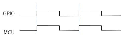
Falling Edge Trigger: The MCU inverts the GPIO level signal and uses it as the interrupt source, triggering on the falling edge.
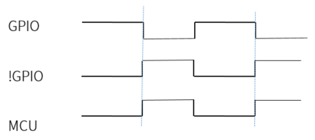
(1) Multiple GPIOs Sharing One Interrupt Source:
Both GPIOs set to rising edge: The MCU ORs the two GPIO level signals and uses the result as the interrupt source, triggering on the rising edge. In the figure below, only GPIO0 triggered the interrupt.
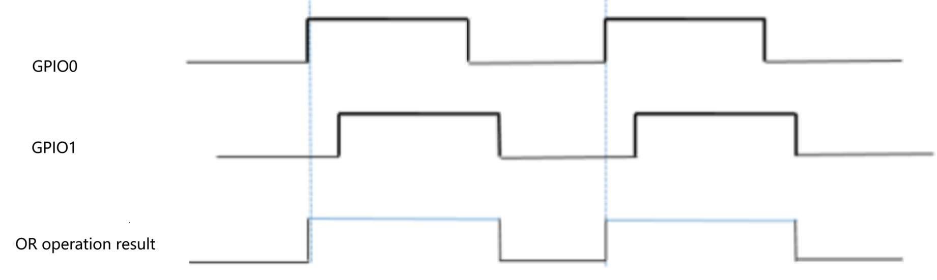
Both GPIOs set to falling edge: The MCU inverts both GPIO level signals, ORs them, and uses the result as the interrupt source, triggering on the rising edge. In the figure below, only GPIO0 triggered the interrupt.
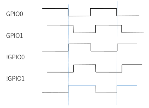
GPIO0 rising edge + GPIO1 falling edge: The MCU inverts GPIO1, ORs it with GPIO0, and uses the result as the interrupt source, triggering on the rising edge. In the figure below, only GPIO1 triggered the interrupt.
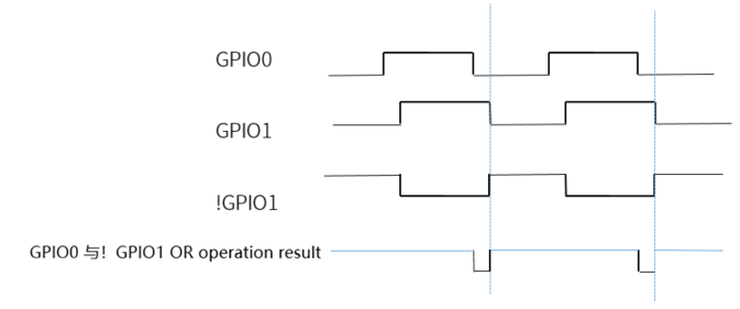
Conclusion: When multiple GPIOs share the same interrupt source, the trigger behavior is unpredictable — not recommended. However, different interrupt sources are independent and can be used simultaneously. For example, if GPIO0 is configured as IRQ0 and GPIO1 as IRQ1, both rising edges trigger interrupts correctly.
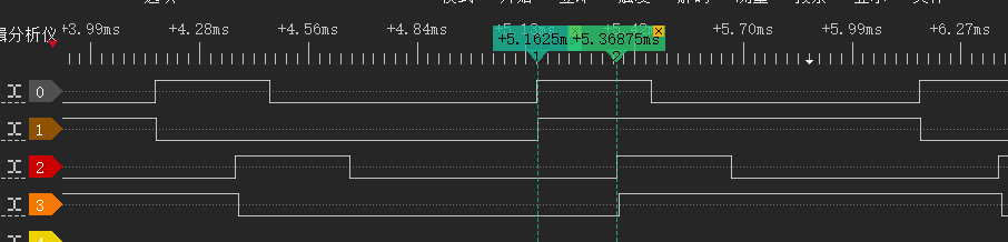
For the actual number of interrupts available on each chip, please see Interrupt Type。
Interrupt Example (Using TL721x as an Example)
The following demonstrates the standard configuration method for the TL721x (Group Select Source Mode) based on the official driver interface:
##include "common.h"

#define IRQ_PIN      GPIO_PA0  // test input pin
#define TEST_LED     GPIO_LED1

volatile unsigned int gpio_src_irq0_cnt = 0;

/**
 * @brief  GPIO_SRC0 Interrupt Service Routine (ISR)
 */
_attribute_ram_code_sec_noinline_ void gpio_src0_irq_handler(void)
{
    gpio_src_irq0_cnt++; // Count interrupt trigger number
    gpio_set_high_level(TEST_LED); // response interrupt

    // Clear the status flag for group interrupt source 0
    gpio_clr_group_irq_status(FLD_GPIO_GROUP_IRQ0);
}
// Register Interrupt Service Routines to the PLIC Vector Table
PLIC_ISR_REGISTER(gpio_src0_irq_handler, IRQ_GPIO_SRC0)

void TL721x_gpio_irq_init(void)
{
    // 1. Configuring Basic General Properties and Input Enable for Pins
    gpio_function_en(IRQ_PIN);
    gpio_output_dis(IRQ_PIN);
    gpio_input_en(IRQ_PIN); // Enable input
    gpio_set_up_down_res(IRQ_PIN, GPIO_PIN_PULLUP_10K); // Config internal 10K pull-up

    // 2. Configuring trigger source and polarity
    gpio_set_src_irq_group(IRQ_PIN >> 8);          // Select the GPIO group to which the pin belongs
    gpio_set_src_irq(IRQ_PIN, INTR_FALLING_EDGE);   // Configured for falling-edge triggering

    // 3. Enable the PLIC channels and global interrupts in the kernel
    plic_interrupt_enable(IRQ_GPIO_SRC0);
    core_interrupt_enable();
}
When using interrupts, we recommend using the built-in API and following the configuration sequence shown in the demo; otherwise, an incorrect configuration sequence may lead to issues such as unintended triggers.
Notes
Digital Pull-up/down Deep Sleep Failure
Some chips provide digital pull-up/pull-down interfaces (such as gpio_set_digital_pullup / gpio_set_digital_pulldown), but digital pull-up/pull-down is only effective in Active mode and becomes inactive upon entering low-power mode. Therefore, pins used as wake-up sources or pins that must maintain a specific voltage level during sleep must use analog pull-up or pull-down (gpio_set_up_down_res).
Wake-up Source Level Maintain
Certain pins on some chips cannot reliably maintain their logic levels in Deep Retention sleep mode (see the comments in the GPIO enumeration in each chip’s gpio.h header file for specific pins). These pins must not be used as sleep wake-up sources, and no external devices with strict level-maintenance requirements should be connected to them.
SWS Debug Pin
The chip uses the SWS interface (typically PA7, though PA3 on some chips) for program download and simulation. If the SWS pin is left floating, external interference may cause its voltage level to fluctuate, leading to leakage in the digital circuitry or even incorrect writing to chip registers, which can result in a system crash.
Solution: Apply a 1M analog pull-up to SWS as soon as possible after the program starts to keep the pin at a fixed voltage level:
gpio_set_up_down_res(GPIO_SWS, GPIO_PIN_PULLUP_1M);
// TC series: gpio_setup_up_down_resistor(GPIO_SWS, GPIO_PIN_PULLUP_1M);
Default Pull-up/down Configuration
The gpio_init(1) uniformly sets the analog pull-up/pull-down for all pins based on the value of the PULL_WAKEUP_SRC_PAx macro (where x is the pin number). This macro has default values defined in gpio_default.h; for some chips, the default is pull-down (e.g., GPIO_PIN_PULLDOWN_100K), while for others, the default is floating (GPIO_PIN_UP_DOWN_FLOAT).
The marco value and definition:
| Macro value | Definition |
|---|---|
GPIO_PIN_UP_DOWN_FLOAT (0) |
Floating (no pull-up/down) |
GPIO_PIN_PULLUP_1M (1) |
1Mohm pull-up |
GPIO_PIN_PULLDOWN_100K (2) |
100Kohm pull-down |
GPIO_PIN_PULLUP_10K (3) |
10Kohm pull-up |
The numbers 10k, 100k, and 1M here are approximate values, not exact values.
Note
- For chips with default pull-down settings, if a pin is actually used for other functions (such as peripheral multiplexing, output driving, or connecting to external pull-up components), the default pull-down setting conflicts with the actual function, resulting in abnormal voltage levels or additional power consumption. Before using the pin, you must redefine the corresponding macro as
GPIO_PIN_UP_DOWN_FLOATto disable the pull-down. This redefinition is performed in the application configuration header files (app_config/*.h):
// Remove the default pull-down for a specific pin in app_config
#define PULL_WAKEUP_SRC_PA0  GPIO_PIN_UP_DOWN_FLOAT
#define PULL_WAKEUP_SRC_PB3  GPIO_PIN_UP_DOWN_FLOAT
When developing, we recommend first checking the default values in the chip’s gpio_default.h file, and then removing the corresponding pull-down settings in app_config based on the pins actually in use.
Analog
Analog overview
The analog register is located in the chip's analog domain and is used to configure simulation-related parameters (such as GPIO input/drive strength, PLL, LDO voltage, etc.). Unlike digital domain registers (which read and write directly via reg_xxx), analog registers require access via dedicated ALG interface modules, which the Analog driver encapsulates.
The driver supports the following access granularities:
| Granularity | TL series | TC series |
|---|---|---|
| Byte (1 byte) | Support | Support |
| Halfword (2 bytes) | Support | Not support |
| Word (4 bytes) | Support | Not support |
| Buffer (batch) | Support | Not support |
Note
- The TL series offers multi-particle interfaces such as
analog_read_reg8/16/32,analog_read_buff; The TC series only offers byte-sizedanalog_read/analog_write(withReadAnalogRegandWriteAnalogRegmacro aliases).
Access interface
Interface naming
| Series | Read (byte) | Write (byte) |
|---|---|---|
| TL | analog_read_reg8(addr) |
analog_write_reg8(addr, data) |
| TC | analog_read(addr) |
analog_write(addr, v) |
The TL series byte read/write interface address parameter is unsigned int (some multi-Bank chips select Bank via the high address position; detailed bit definitions are found in each chip's analog.h); The TC series address parameter is unsigned char.
Concurrent protection
The analog read/write interface has interrupts disabled internally (TL series uses core_interrupt_disable, TC series uses irq_disable). A single read/write is an atomic operation that can be safely called in interrupt contexts.
Use examples
/* Read-Rewrite: Set a certain bit */
analog_write_reg8(0x3b, analog_read_reg8(0x3b) | BIT(7));

/* Write directly */
analog_write_reg8(0x3c, 0x5A);
Stores analog registers
Based on whether the register values are maintained under several typical different behaviors, storage analog registers are divided into two categories:
| Type | power on | 32K watchdog | timer watchdog | reboot | deep | deep retention |
|---|---|---|---|---|---|---|
| PM_ANA_REG_WD_CLR_BUF | Restore default values | Restore default values | Restore default values | Restore default values | Maintain | Maintain |
| PM_ANA_REG_POWER_ON_CLR_BUF | Restore default values | Restore default values | Maintain | Maintain | Maintain | Maintain |
The core difference between the two types of registers lies in the timer watchdog and reboot scenarios:
- WD_CLR_BUF: Any reset will restore the default value, suitable for storing data that "all scenarios require reinitialization" to avoid interference with old data.
- POWER_ON_CLR_BUF: Keeps the default value of the timer watchdog and reboot not restored, which can be used to distinguish between "power-on/32K watchdog reset" and "timer watchdog/software reset."
Important
- Each chip's memory register address, quantity, reset source, and initial value are all different. When using, you must refer to the
PM_ANA_REG_* macro definitions and comments in eachchip's pm.hfor reference. Do not copy the address across chips.
Before use, check the comment notes for the corresponding registers in pm.h to confirm which bits are available. Before first use, it is recommended to specify the expected initial value rather than relying on the default.
Notes
-
DMA mode is not recommended: TL series analog drivers provide DMA channel configuration macros, but after DMA configuration returns, the actual transfer may not be complete. If the analog register is accessed again during the interrupt, DMA transmission may be interrupted, creating unknown risks. It is not recommended to use DMA to read and write analog registers.
-
write_buff length limit: TL series
analog_write_buffsingle write length cannot exceed 8 bytes. -
Bit Occupation Avoidance: Before accessing the storage analog register, be sure to check the comments for the corresponding register in
pm.hto confirm that the target bit is not being occupied by drivers. -
Address is based on pm.h: memory register address, reset behavior, and initial values vary by chip. Do not copy addresses across chips.
Flash
Flash type
Built-in Flash
Telink ICs generally have multiple built-in Flash from different manufacturers, and a single manufacturer's Flash may have different types (different Flash capacities). The built-in Flash model is not static; at some point, a new type may be added. The Platform SDK ensures that the driver code corresponding to that Flash model is added immediately to guarantee mass production for customers.
For different chips with built-in Flash types, users can check the embedded Flash types of the relevant chip using the following method. What you see is all the Flash types currently supported by the SDK:
Reference: chip/<model>/drivers/flash/flash_type.h
The Telink Platform SDK implements some of the most basic functions based on Flash datasheets, meeting the needs of the vast majority of users. The content on the Flash datasheet is public; this document does not repeat the content of the datasheet. Therefore, it is recommended that customers proactively read the Flash datasheet after learning the built-in Flash model to understand technical details. First, it provides more debugging methods and information when problems arise (such as using the Flash status register content to trace issues); second, users can develop and implement some unconventional features themselves (such as customizing protection policies).
User-customized Flash
For all built-in Flash types, both hardware and software have been thoroughly evaluated and tested. In addition to basic read, write, and erase functions, the evaluation and testing also include operating time, temperature fluctuations, power-on/off data, and other data and performance. Therefore, the Flash models included in the Platform SDK are safe to use.
Telink does not recommend customers add new Flash models. If a customer insists on adding a particular Flash model, verifying that the basic functions of read, write, and erase are correct is not enough. We believe that the capability to conduct a comprehensive evaluation and testing of a single Flash device is very important. Therefore, contact our FAE for communication and request our original factory to conduct evaluation and testing. Only the Flash types we evaluate and pass testing can be used in mass production.
Summary table of chip functional differences
The differences in Flash functionality among chips are summarized as follows:
| Chips | Multi slaves | Four-line mode | Encrypted read/write |
|---|---|---|---|
| B80 / B85 / B87 | × | × | × |
| TC321x / TC122x / TC123x / TC1211 | × | × | × |
| B91 | × | √ | × |
| B92 | × | √ | √ |
| TL321x | × | √ | √ |
| TL323x | × | √ | √ |
| TL521X | × | √ | × |
| TL721x / TL322x / TL751x | √ | √ | √ |
STACK_SIZE_FOR_FLASH_DATA: The maximum write length per pass for buf to a Flash address. The default is 256 bytes for the TL series, and the default for the TC series is 32 bytes.
Flash bus address space
General address mapping rules:
- Flash address base offset:
FLASH_ADDR_BASE = 0x20000000 - All
addrparameters for all Flash APIs do not require base address 0x20000000, ranging from 0 to the size of Flash storage space.
Multi-slave device address space:
Supports up to 4 Flash devices (SLAVE0~SLAVE3), with a total access space of 64MB. The address space of each slave's is divided using the mspi_slave_device_addr_space_config() interface. addr parameter for Flash interface = actual Flash access location + Slave base address.
Note
- For the Flash bus address space layout diagram, please refer to the introduction to the basic module.
Support status for each chip's multi-slave
For the multi-slave support status of each chip, see the "Chip Function Difference Summary Table."
Note
- The following APIs have corresponding
_with_device_numversions for multiple Slave chips, used to specify the Slave device for operation. For simplicity, this document uses the single Slave API as an example.
Flash storage address allocation
Flash storage space is available to both SDKs and user applications. To ensure users do not experience conflicts when using Flash, the Flash storage space already occupied by each Telink SDK is introduced below. After learning these rules, users try to avoid these areas.
To make SDK address space allocation easier and more convenient for unified management across all Telink chip series and all product categories, all Flash address allocation rules are based on Flash Capacity.
Allocation of MAC Address and Calibration areas
All Telink SDKs uniformly follow the address allocation as follows. MAC Address can be used for general protocols such as BT/BLE/Zigbee; Thanks to its unique ID feature, users can also customize other SDKs and applications according to their own needs. Calibration can refer to the details of the corresponding chapter.

Note
- MAC Address and Calibration address allocation are standards followed across all Telink software, and are the same across all SDKs (such as Platform SDK, BLE SDK, 2.4G SDK, etc.).
Firmware Signature feature Flash space usage
Firmware Signature is an Optional feature.
- Some chips support hardware Secure Boot functionality, and their Descriptor occupies specific storage space. For details, refer to the Secure Boot section.
- Some chips implement software Firmware Signature solutions, storing Signature values at special Flash addresses. For details, refer to the relevant SDK documentation.
Higher-level SDK occupies additional space
The above is the Flash usage situation understood from the perspective of the General Platform SDK. In addition, various general protocol SDKs (such as Bluetooth/Zigbee SDKs) continue to consume some space as system usage due to their functional requirements (such as bootloader/OTA functions, Bluetooth pairing and binding). Users should refer to the Handbook introductions for these SDKs for more information.
MID and UID
MID
Flash MID = Manufacturer ID, which is the manufacturer identification code for SPI Flash chips.
Obtained via flash_read_mid(), containing capacity and manufacturer information. The meanings of each byte are as follows:
| Byte | Meaning |
|---|---|
| High Byte | Flash capacity labeling (see table below) |
| Medium byte + low byte | Vendor + process architecture information |
For example, 0x166085:
- High Byte
0x16: capacity is 4MB - Low 16-bit
0x6085:P UYA manufacturer, SONOS process
| MID capacity labeling | Corresponding Flash capacity |
|---|---|
| 0x10 | 64KB |
| 0x11 | 128KB |
| 0x12 | 256KB |
| 0x13 | 512KB |
| 0x14 | 1MB |
| 0x15 | 2MB |
| 0x16 | 4MB |
| 0x17 | 8MB |
| 0x18 | 16MB |
flash_vendor_e Definition
The flash_vendor_e high 8-bit is based on Mid's low 16-bit Flash vendor and process architecture information, used to identify different Flash process architectures. Below is a summary of all entries:
typedef enum {
    FLASH_ETOX_ZB    = 0x0100325E, // 325E     bit[24]=1:ETOX
    FLASH_ETOX_GD    = 0x010060C8, // 60C8/4051
    FLASH_ETOX_PUYA  = 0x01002085, // 2085
    FLASH_SONOS_PUYA = 0x02006085, // 6085     bit[25]=1:SONOS
    FLASH_SONOS_TH   = 0x020060EB, // 60EB
    FLASH_SST_TH     = 0x040060CD, // 60CD     bit[26]=1:SST
    FLASH_NORD_GT    = 0x100060C4, // 60C4     bit[27]=1:NORD
    FLASH_NORD_TH    = 0x100070CD, // 70CD/71CD/51CD bit[27]=1:NORD
} flash_vendor_e;
Note
- The enumeration entries supported by different chips may not be exactly the same; please refer to the
flash.hof the corresponding chip.
Read the mid API
unsigned int flash_read_mid(void);
Usage example:
g_flash_mid = flash_read_mid();
Obtain the vendor API
unsigned int flash_get_vendor(unsigned int flash_mid);
Function: Retrieves Flash manufacturer and process information based on MID and returns flash_vendor_e type values. This value contains the Flash process type (ETOX/SONOS/SST) and vendor information.
Vendor information is linked to software functions
Differences in Flash characteristics across different processes:
| Process | Features | Write time characteristics |
|---|---|---|
| ETOX | bit[24]=1 | Byte Program Time ≠ Page Programming Time |
| SONOS | bit[25]=1 | Byte Program Time == Page Programming Time |
| SST | bit[26]=1 | Byte Program Time ≠ Page Programming Time |
| NORD | bit[27]=1 | Byte Program Time ≠ Page Programming Time |
SONOS process Flash also takes longer to write per byte than ETOX. To avoid related errors, the timing design of BLE SDKs based on TC series chips requires special handling. For details, refer to the Handbook corresponding to the BLE SDK. If a user's SDK or application has similar issues, targeted evaluation and handling are needed during the design process.
Capacity information associated with software functions
From the introduction to the Flash storage address allocation section, it is clear that MAC addresses and calibration functions require reading capacity information in advance before performing corresponding operations at the corresponding addresses.
UID
Flash UID = The unique hardware identifier for the flash memory chip, which is a globally unique identifier that is solidified by the manufacturer's laser/process at the factory for SPI/xSPI NOR Flash.
Due to its uniqueness and immutability, it can be used for chip identity authentication, firmware encryption, anti-cloning, product traceability, production control, and more.
Read the UID APIs
void flash_read_uid(unsigned char idcmd, unsigned char *buf);
Function: Reads the unique hardware identifier (UID) of Flash. The returned UID length depends on the specific Flash model, usually 16 bytes.
UID commands: Different vendors may have different Flash UID reading commands. Most vendors (PUYA, GD, ZB, TH) use 0x4b commands, while a few vendors (XTX) use 0x5a commands. flash_read_uid The API requires users to explicitly pass in the idcmd parameter, which distinguishes between vendors.
Mid and Uid validation APIs
int flash_read_mid_uid_with_check(unsigned int *flash_mid, unsigned char *flash_uid);
Function: Reads both MID and UID of Flash simultaneously and verifies their correctness.
Return value:
1: The Flash model is known and UID reading is successful0: Flash has no UID or an unknown models
Description: This function iterates through the SDK-supported Flash list, matches MID, reads UIDs, and checks whether UIDs are empty (all in 0x5101 mode means no UIDs).
On the Platform SDK and some upper-layer SDKs (such as the BLE SDK), software Firmware Signature solutions have been implemented for certain chips, utilizing UID uniqueness as part of the key to participate in signature computation.
Basic Flash operations
Four-line mode
Compared to the two-line mode, Flash's four-line mode offers faster read/write speeds but higher instantaneous power consumption.
For the support status of each chip's four-line functionality, see the "Chip Function Difference Summary Table."
Enable four-line mode. Example code is as follows:
unsigned char flash_set_4line_read_write(unsigned int flash_mid)
{
    unsigned char status = flash_4line_en(flash_mid);
    if (status == 1) {
        flash_read_page = flash_4read;
        flash_set_xip_config(FLASH_X4READ_CMD);
        flash_write_page = flash_quad_page_program;
    }
    return status;
}
Flash Read (non-encrypted)
(1) Standard reading flash_read_page
extern flash_handler_t flash_read_page;
flash_read_page is a function pointer, which by default points to a standard read function and can be switched to other read modes via flash_change_rw_func().
Usage method:
flash_read_page(addr, len, buf);
(2) Dual-line reading flash_dread
_attribute_text_sec_ void flash_dread(unsigned long addr, unsigned long len, unsigned char *buf);
Function: Uses dual I/O mode to read data from Flash.
(3) Four-wire reading flash_4read
_attribute_text_sec_ void flash_4read(unsigned long addr, unsigned long len, unsigned char *buf);
Function: Reads data from Flash using Quad I/O mode.
(4) Read operation precautions
- Supports reading any address within Flash capacity
- The read
length lencannot be 0 - The maximum read length does not exceed the RAM allocated space and Flash capacity
Flash Write (non-encrypted)
(1) Standard write flash_write_page
extern flash_handler_t flash_write_page;
Similar to flash_read_page, flash_write_page is a function pointer that can be switched via flash_change_rw_func().
(2) Single-line page writes flash_page_program
void flash_page_program(unsigned long addr, unsigned long len, unsigned char *buf);
Function: Writes data to Flash in standard SPI mode (single-wire).
(3) Four-line page write flash_quad_page_program
void flash_quad_page_program(unsigned long addr, unsigned long len, unsigned char *buf);
Function: Writes data to Flash in quad mode for faster speed.
(4) Write operation precautions
- The write length
lencannot be 0 - Supports cross-page writing, with
lenvalues exceeding 256 bytes (single page size) - The
bufpointer should be an SRAM address. If a Flash address is passed, the driver will automatically copy the data to the stack before writing it. At this time, the single write length cannot exceedSTACK_SIZE_FOR_FLASH_DATA(default values are shown in the "Chip Function Difference Summary Table") - It is not recommended to write with bytes (<=255 bytes). If users want to write with one or more bytes (<=255 bytes), please follow the instructions below:
- Make sure the number of written bytes after erasing does not exceed 64
- In a page, byte can only be used once after writing to a page, and only supports writing from "1" to "0"
- Before writing, you must ensure the target area has been erased (after erasure, it is 0xFF); otherwise, the write may fail.
Flash Erase
(1) Sector Erasure (4KB)
_attribute_text_sec_ void flash_erase_sector(unsigned long addr);
- Address requirements: Must be a multiple of 0 or 0x1000
- Erase size: 4KB
(2) 32KB block erasure
_attribute_text_sec_ void flash_erase_block_32k(unsigned long addr);
- Address requirements: Must be a multiple of 0 or 0x8000
- Erase size: 32KB
(3) 64KB block erased
_attribute_text_sec_ void flash_erase_block_64k(unsigned long addr);
- Address requirements: Must be a multiple of 0 or 0x10000
- Erase size: 64KB
Note
- Block erasing takes a long time, so please feed dog in advance. For the maximum block erase time, please refer to the Flash datasheet.
Encrypted read/write
Only some chips that support Firmware Encryption have encrypted read/write capabilities. For applications using Firmware Encryption, read and write operations must use APIs related to encrypted read/write.
Supported chips: See the "Encrypted Read/Write" column in the "Chip Function Difference Summary Table".
(1) Encrypted writes
//Single-line encrypted page write
void flash_page_program_encrypt(unsigned long addr, unsigned long len, unsigned char *buf);

//Four-line encrypted page writing
void flash_quad_page_program_encrypt(unsigned long addr, unsigned long len, unsigned char *buf);
Function: Writes data to Flash in encrypted mode. The data written is encrypted by a hardware encryption engine before being stored.
(2) Decryption and readout verification
//Dual-line decryption and read verification
unsigned char flash_dread_decrypt_check(unsigned long addr, unsigned long plain_len, unsigned char *plain_buf);

//Four-line decryption and read verification
unsigned char flash_4read_decrypt_check(unsigned long addr, unsigned long plain_len, unsigned char *plain_buf);
Return value:
0: Check passed (read decrypted data matches expected plaintext)1: Check failure
Function: Read encrypted data from Flash, automatically decrypt it, and compare it with the provided plaintext buffer to verify whether the encrypted data is correct.
Function pointer versions:
extern flash_read_check_handler_t flash_read_page_decrypt_check;  //Decrypt and read the checksum function pointer
extern flash_handler_t            flash_write_page_encrypt;       //Encryption writes function pointers
Flash safe operations
In embedded systems, Flash erase and write operations carry a high risk of failure, so secure Flash operations are crucial. Flash uses the SPI interface for data communication. Although the SPI protocol itself has good transmission stability, when the SoC is powered on or off, operates under special conditions, or when the VBAT supply voltage approaches the Flash operating threshold, the system is prone to large power supply fluctuations, which can cause abnormal jitter in the SPI clock and data signals, resulting in unauthorized tampering of address erases/writes or data. Among them, Flash erasure is a time-consuming operation, with a longer window of interference and increased risk. At the same time, if the software logic design is complex, address calculation links are cumbersome, and combined with human oversight during development, it can lead to anomalies in erasing addresses and data, and even illegal overwriting of firmware partitions. Once these issues occur, they cause irreversible software damage, not only causing standalone functions to fail but, in severe cases, trigger product disassembly, firmware reburning, and batch recalls, resulting in high operational costs and economic losses for enterprises.
To ensure the safe operation of Flash application products, Telink provides multiple effective protection and avoidance measures at both the hardware and software levels. Users are strongly encouraged to adopt these measures to enhance product stability.
Flash protection
(1) Flash's own protective features
The Flash chip itself provides a Status Register protection mechanism, implementing write protection for different regions by setting the Block Protect bit in the Status Register. Different Flash models support different locking zones.
The protection interfaces for each Flash model follow the flash_lock_<mid>(<lock_type>) and flash_unlock_<mid>() naming conventions, with the specific supported lock types defined in the header files corresponding to each Flash model (e.g., flash_mid146085.h).
Example of enumeration of protected areas:
//Different Flash models offer different lock area options, such as:
FLASH_LOCK_LOW_64K // Low address 64KB protection
FLASH_LOCK_LOW_128K // Low address 128KB protection
FLASH_LOCK_LOW_256K // Low address 256KB protection
FLASH_LOCK_ALL      // Whole Protection
Usage example:
// 1. Lock Flash
flash_lock_mid146085(FLASH_LOCK_LOW_64K_MID146085);

// 2. Verify the locking effect: erase and write to check if the data is correct
flash_erase_sector(FLASH_ADDR);
flash_write_page(FLASH_ADDR + 0x80, FLASH_BUFF_LEN, (unsigned char *)Flash_Write_Buff);
flash_read_page(FLASH_ADDR + 0x80, FLASH_BUFF_LEN, (unsigned char *)Flash_Read_Buff);
//If the data matches expectations, the lock is active (the protected area remains unchanged).

// 3. Unlock Flash
flash_unlock_mid146085();

// 4. Verify unlocking effect: After erasing, the read should be 0xFF
flash_erase_sector(FLASH_ADDR);
flash_read_page(FLASH_ADDR + 0x80, FLASH_BUFF_LEN, (unsigned char *)Flash_Read_Buff);
//If the data is 0xFF, it means the unlock was successful
Path: The protection interface definitions for each Flash model are located in the flash_mid*.h file under the chip/<models>/drivers/flash/ directory.
(2) Flash default protection logic during chip initialization
During the chip power-on initialization (platform_init), the SDK automatically executes Flash recognition and default protection logic. The process is as follows:
- Read MID and match the Flash model
hal_flash_init() calls flash_read_mid() to read Flash's MID, then iterates the match in flash_list[] (defined in chip/<model>/drivers/flash/flash_common.c). If no match is found, initialization fails (returns non-zero), and the program enters a while(1) deadloop.
- Half the space is locked by default
After successful matching, hal_flash_lock() checks whether the current Flash is locked; if not, it calls lock_func(lock_size) by default, locking the lower address half of the space. The default protection size for each capacity is as follows:
| Flash capacity | Default protection size |
|---|---|
| 512KB | Low 256KB |
| 1MB | Low 512KB |
| 2MB | Low 1MB |
| 4MB | Low 2MB |
| 8MB | Low 4MB |
| 16MB | Low 8MB |
Note
- Protecting the low-address area means protecting the Firmware code area; the high-address area is reserved for user data read/write.
- Match failure processing
If there is no matching MID in flash_list[], g_mid_matched is false, hal_flash_init() returns 1, and the upper layer uses the while(1) infinite loop to indicate that the Flash model is not supported.
Customize protection size
To change the default protection size, follow these steps:
- Define macro
FLASH_PROTECT_MODIFY_CONFIGincommon.has 1. - In
common.cflash_init_list[], add target MIDs andblock_sizeby chip models. - Only the firmware area is protected, not the data area, to avoid frequent unlocking that could wear the Status Register.
Low Battery Detect
Battery power detect/check may also appear under other names in the Telink SDK and related documentation, including: battery power detect/check, low battery detect/check, low power detect/check, and battery check detect/check, etc.
This document is described under the name "Low Battery Detect."
For battery-powered products, as the battery capacity gradually decreases, when the voltage drops to a certain value, many problems arise:
- For example, for an SoC with a voltage range of 1.8V~3.6V, stable operation cannot be guaranteed when the voltage is below 1.8V.
- When the battery voltage is low, due to unstable power supply, SPI bus data jitter may occur during Flash write and erase operations, causing abnormal overwriting of Flash.
The main functions of low voltage detection for battery-powered products are as follows:
- Generally, ADC is used in the main program loop, the ADC periodically samples the VBAT values.
- Notes: To avoid ADC detection being affected by power supply jitter (for example, coinciding with RF transmission and reception), it is recommended to use multiple ADC sampled data for smoothing filtering algorithms.
- Set a Secure Voltage so that the MCU is only allowed to continue operating when the voltage exceeds this secure voltage; Once the voltage falls below the safe limit, the MCU stops running and needs to be shut down immediately (this can be achieved by entering modes like suspend or deepsleep).
Currently, the Platform SDK does not provide a reference design for low battery detection. Telink upper-level SDKs, some SDKs add reference designs for low battery detection (such as BLE SDKs), allowing users to refer to and implement them; Other SDKs without this reference design can be developed and implemented by users based on the main features mentioned above.
Power-on/off protection function
(1) Functional background
Flash risks during SoC power-on/off:
- Moment of power-on: unstable power supply, SPI clock/data jitter, MCU mistakenly sends erase commands, firmware or boot area damaged.
- Power off process: erase (takes tens~hundreds of ms) or power loss during programming, block or page half-write, data disorder, Flash bricking.
- Voltage threashold: Vbat approaches the Flash operating threshold, SPI signal jitters, and address/data is modified.
- Repeated power up/down: power ripple + frequent resets, worsening timing errors and increased wear.
The ADC-based low power detection solution protects Flash operation safety during the program's main cycle time and cannot cover protection during the MCU power-on and power-off phases. Therefore, Telink is gradually introducing LPC (Low Power Comparison) to protect SoC power-on and power-up, while also considering the program's main cycle time.
(2) Solution evolution and differences in chips
Some chips offer power-on and down-power protection solutions, while other older chips lack this feature due to historical reasons. Users can refer to existing solutions to independently develop and implement the same functionality. The differences among chip solutions are shown in the table below:
| Chip model | Solution type | Software required | Trigger method | Behavior |
|---|---|---|---|---|
| TL321x | Software solutions | Yes | LPC interrupt | Triggers interrupts at low voltage, pulling the MCU and MSPI during interrupts |
| TL322x | Hardware solutions | No | LPC → PEM → DMA | Automatically triggered at low voltage, pulling the MCU and MSPI through PEM channel + DMA write register |
| TL323x | Hardware Solutions (Optimization) | No | Direct detection of LPD module | A new LPD module has been added to directly detect VBAT. When the voltage is below 1.7V, hardware automatically triggers to pull the MCU or MSPI (optional), with both simultaneously held by default. |
(3) Details of different solutions
TL321x (software solution).
- Configure any GPIO output high level among PB1~7 (cannot be used as another function after selection)
- The PBx pin level is detected via LPC, and the VBAT voltage is detected indirectly
- When the voltage drops below about 2.0V, an LPC interrupt is triggered, pulling the MCU and MSPI in the interrupt service program.
The scope of impact of enabling this feature:
- Chip power supply range: only supports 2.1V - 4.2V.
- Interrupt preemption: The total interrupt enable
core_interrupt_enable()must be called by the user themselves and should be called as early as possible to maximize the duration of Flash protection. - Interrupt priority: LPC interrupt priority (for Flash power-off protection function) > Flash operation priority> Other interrupt priority.
- GPIO usage: One GPIO is required, default is PB4. Users can freely select PB1~7 based on actual application. Once selected, the GPIO cannot be used for other functions.
TL321x is disabled by default; users need to consider enabling it based on actual application scenarios and the above range of impact.
Reference code path: FLASH_LPC_PROTECT_MODE in \demo\vendor\Flash_Demo
TL322x (hardware solution).
- Also configure any GPIO output high level from PB1~7 (cannot be used as another function after selection)
- The PBx pin level is detected via LPC, and the VBAT voltage is detected indirectly
- When the voltage drops below about 2.0V, the LPC triggers the DMA write register through the PEM channel
- DMA hardware automatically holds the MCU and MSPI without software interrupts
The scope of impact of enabling this feature:
- Chip power supply range: only supports 2.1V - 4.2V.
- GPIO Occupancy: One GPIO from PB1~7 must be occupied; this GPIO cannot be used for other functions.
- PEM Occupancy: One PEM channel must be occupied, and this PEM cannot be used for other functions.
- DMA Occupancy: One channel between DMA0~7 must be occupied; this DMA cannot be used for other functions. 。
TL322x This feature is disabled by default. If users need high-speed applications with a main frequency of D25F CLOCK > 96MHz and can accept the above impact range, this feature must be enabled to improve chip robustness during high-speed operation. Please contact Telink FAE for support.
Functional interface path: lpc_pem_flash_prot_config() in \chip\tl322x\drivers\lpc.c
TL323x (optimized hardware solution).
- A new LPD module has been added to directly detect VBAT voltage, no need for GPIO indirect detection
- When the VBAT voltage drops below about 1.7V, hardware automatically triggers the pull on the MCU and MSPI
- No software intervention required throughout the process, resulting in faster and more reliable response
TL323x This feature is enabled by default, allowing users to use it directly without any configuration.
Note
- During chip operation, power supply fluctuations, voltage glitches during the first power-on or wake-up may cause voltage to fall below the trigger threshold, accidentally triggering LPC/LPD protection and causing the chip to jam. When using the above solutions, users must enable the 32K Watchdog or Timer Watchdog to prevent false triggers that could prevent the chip from recovering for a long time.
Power Management System
When the MCU is running programs normally, it operates in working mode, and the current remains at the mA level. When PM activates it into low-power sleep mode, the current is only at the uA level, greatly reducing power consumption. In low-power mode, except for the modules and clocks needed to wake up, all other modules and clocks are powered off. Some modules that require voltage maintenance also use low-power LDO holding voltages, which cannot operate properly.
Function description
Five low-power modes
Low power mode, also known as sleep mode, has five types:
- Suspend: Pause mode
- Deep sleep without SRAM retention (abbreviated as DeepSleep): deep sleep without SRAM retention
- Deep sleep with SRAM retention (abbreviated as DeepSleep Retention / Retention): deep sleep with SRAM retention
- WFI (Wait For Interrupt): Wait for interrupt mode
- Shutdown: Shutdown mode
Suspend:
In Suspend mode, program execution is paused, similar to a pause function. After the chip wakes up from Suspend mode, the program resumes execution. In Suspend mode, the PM module operates normally. The SRAM remains powered and retains all data. All analog registers remain powered, while a small number of digital registers are powered off. To reduce power consumption, software can power down modules such as RF, USB, and Audio. In this case, the corresponding digital registers of these modules are lost. For example, the RF module must be reinitialized after waking up before it can transmit packets. All other registers are retained. To enable packet transmission immediately after wake-up, do not power down the corresponding modules. However, this results in higher power consumption. The chip can be woken up by sources such as GPIO and timers.
DeepSleep:
In DeepSleep mode, program execution stops, and most hardware modules in the MCU are powered down. When the chip is awakened from DeepSleep, it restarts from the hardware bootloader (equivalent to a power-on reset), and the program re-initializes from the beginning. In DeepSleep mode, the PM module operates normally, SRAM loses data when powering down, most 3.3V analog registers are retained, while other analog registers and all digital registers lose power. The chip can be woken up by sources such as GPIO and timers.
DeepSleep Retention:
DeepSleep mode has very low current, but cannot store SRAM information; In Suspend mode, SRAM and registers can be kept intact, but the current is relatively high. To enable scenarios where sleep current is very low but can be immediately restored after waking, a DeepSleep Retention mode has been added. DeepSleep Retention mode is more similar to DeepSleep mode. The only difference from DeepSleep is that DeepSleep Retention allows a portion of SRAM to be selectively retained. The larger the retained SRAM area, the higher the power consumption.
In DeepSleep Retention mode, program execution stops, and most hardware modules in the MCU are powered down. When the chip is awakened from DeepSleep Retention, the MCU starts running from the software bootloader (not the hardware bootloader), and the program resumes initialization. In DeepSleep Retention mode, the PM module operates normally; a portion of the SRAM is kept powered, while the rest is powered down. Most 3.3V analog registers are retained, while the remaining analog registers and all digital registers are powered down. The increase in current consumption compared to DeepSleep mode is solely due to the current consumed by the SRAM retention circuit. The chip can be woken up by sources such as GPIO and timers. Compared to DeepSleep mode, DeepSleep Retention retains SRAM content. Therefore, upon wake‑up, the chip can directly boot from the retained SRAM, eliminating the need to copy code/data from Flash to RAM, resulting in a faster wake-up.
WFI:
WFI (Wait For Interrupt) is the lightest low‑power mode. The MCU only pauses instruction execution (CPU clock gating) without powering down any modules. All power supplies and clocks remain unchanged. SRAM, digital registers, and analog registers are all retained without data loss, and no peripheral controllers are reset. When any enabled interrupt is triggered, the MCU immediately resumes execution after the WFI instruction, requiring no restart or any resumption/reinitialization operations.
WFI has the highest power consumption among the five low-power modes, still lower than normal operating mode, but has the lowest wake-up latency. Suitable for short-term idle scenarios requiring rapid response to interruptions.
Precautions:
- Before entering WFI, you must ensure that at least one interrupt source is enabled; otherwise, the MCU will permanently hang and cannot be woken up.
- If the watchdog is enabled and the dog cannot be serviced during WFI, make sure the wake-up cycle is less than the watchdog's timeout
Shutdown:
Shutdown mode is the low-power mode with the lowest power consumption. In Shutdown mode, all modules of the MCU are powered down, including SRAM, all digital registers, and all analog registers; all of which lose their contents. The PM module itself is also powered off, with only a minimal amount of analog wake‑up circuitry remaining active. Wake-up sources only support PAD wake-up; other wake-up sources (Timer/MDEC/LPC/CORE) are not available. Only some chips support Shutdown mode; refer to the enumeration pm_sleep_mode_e or SleepMode_TypeDef for the corresponding chip.
When the chip wakes up from Shutdown, the MCU behaves the same as a fresh power‑on reset. It restarts from the hardware bootloader, and all SRAM and registers must be re‑initialized. Suitable for scenarios requiring long, extremely low-power standby periods.
Precautions:
- All states are lost after wake‑up from Shutdown. Therefore, before entering Shutdown, any data that needs to be retained must be persisted to external storage (such as Flash).
- Only the PAD can wake up the chip from Shutdown. Before entering Shutdown, the PAD wake‑up source and its pull‑up/pull‑down configuration must be properly set.
Differences:
Differences between WFI and Suspend:
- WFI does not call sleep functions, does not enter the PM module's power management workflow, does not switch LDOs, and does not power down any modules. Suspend invokes the PM module to power down specific modules and perform LDO switching.
- The wake-up source of WFI is any enabled interrupt (such as GPIO interrupt, Timer interrupt, UART interrupt, etc.), not limited to the wake-up source defined by PM.
- After waking up from WFI mode, execution resumes directly without any recovery operations. After waking up from Suspend mode, some powered-down modules (such as the RF module) may need to be reinitialized.
Differences between Shutdown and DeepSleep:
- Shutdown has a more extensive power-down scope than Deep Sleep. In Deep Sleep mode, the PM module and most 3.3 V analog registers remain powered, whereas Shutdown mode powers down all of them.
- Shutdown supports only PAD wake-up, whereas Deep Sleep also supports other wake-up sources, such as timers.
- Both modes restart through the hardware bootloader after wake-up, but Shutdown has a longer wake-up latency than Deep Sleep.
Differences between DeepSleep and DeepSleep Retention:
- In Deep Sleep mode, all SRAM is powered down. In Deep Sleep Retention mode, a portion of the SRAM remains powered, and the size of the retained SRAM region can be configured independently for each core.
- After waking up from Deep Sleep mode, the chip restarts from the hardware bootloader and boots from Flash. After waking up from Deep Sleep Retention mode, the chip starts from the software bootloader and can boot directly from the retained SRAM, eliminating the need to reload code and data from Flash, thereby reducing wake-up latency.
Low-power mode workflow
Different sleep modes result in inconsistent MCU operation processes. Below is a detailed introduction to the MCU operation process after waking up in the five sleep modes: WFI, Suspend, DeepSleep, DeepSleep Retention, and Shutdown. Refer to the figure below.
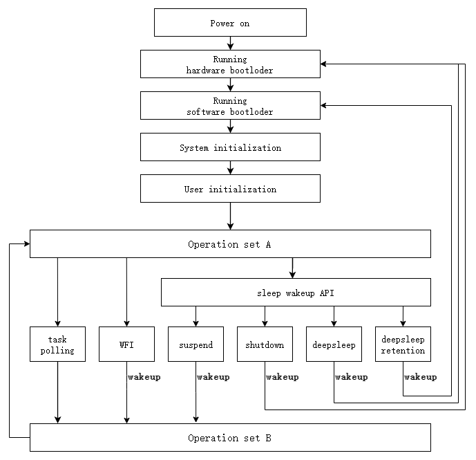
The modules in the flowchart are described as follows:
- Running hardware bootloader: MCU hardware performs fixed operations fixed in the ROM, which cannot be modified by software, usually including wake-up flash and other operations. ROM implementations vary across different chip series.
- Run software bootloader: After the hardware bootloader finishes, it starts running the software bootloader, which is the assembly code that starts after interrupting the vector segment. Its purpose is to set up the memory environment for running C language programs and complete memory initialization. The boot process varies by chip series: After waking up from Deep Sleep mode, the chip typically boots from Flash, while after waking up from Deep Sleep Retention mode, it can boot directly from the retained SRAM.
- System initialization: Initialize each hardware module such as
sys_initandclock_initin the main function, and set the register status of each hardware module. - User initialization: Corresponding to
user_initand other user initialization functions. - main_loop: After initialization, enters the while(1) main loop. The operation before entering sleep mode in the main loop is called "Operation Set A"; the operation after sleep wake-up is called "Operation Set B".
Process analysis of each sleep mode:
| Mode | Behavior after wake-up | SRAM | Register | Recovery requirements |
|---|---|---|---|---|
| Normal polling | Loop Operation Set A -> B | - | - | None |
| WFI | After an interrupt is triggered, execution resumes directly from the instruction following the WFI instruction. | 100% retained | 100% retained | None |
| Suspend | pm_sleep_wakeup() returns normally, continuing to execute Operation Set B |
100% retained | mostly retained | Little or no recovery required |
| DeepSleep Retention | Starts execution from the software bootloader | Partially retained | Mostly lost | Almost complete reinitialization required |
| DeepSleep | Similar to a cold boot; restarts from the hardware bootloader | 100% lost | Mostly lost | Full reinitialization required |
| Shutdown | Complete power-down; restarts from the hardware bootloader | 100% lost | 100% lost | Full reinitialization required |
Breaking down the registers in the table above, the states of SRAM, digital registers, and analog registers in five low-power modes are as follows:
| Mode | SRAM | Digital register | Analog Register (1V) | Analog Register (3V) |
|---|---|---|---|---|
| WFI | 100% retained | 100% retained | 100% retained | 100% retained |
| Suspend | 100% retained | C1 | 100% retained | 100% retained |
| DeepSleep Retention | C2 | 100% lost | 100% lost | 100% retained |
| DeepSleep | 100% lost | 100% lost | 100% lost | 100% retained |
| Shutdown | 100% lost | 100% lost | 100% lost | 100% lost |
C1: Most registers remain unchanged, with only a few special registers as exceptions. In Suspend mode, the power supply to modules such as RF, AUDIO, and USB can be selectively retained. The corresponding register contents are retained or lost accordingly.
C2: In DeepSleep Retention mode, the SRAM retention size is selectable; the SRAM retention size for each core is specified by pm_sleep_mode_e enumeration. Different chips have different selectable ranges; refer to the enumerated definitions for each chip.
Multi-core sleep and wake-up
Applicable Notes: This chapter only applies to chips that support multi-core. For specific chips supporting multi-core, please refer to the Overview section. This chapter is not applicable to single-core chips.
Classification of multi-core chip cores:
- Main core:D25F, the main control core, runs the main program, controls the power for the entire chip; the main core cannot be powered down individually.
- Secondary cores: DSP and N22 (RISC-V coprocessor), can be powered down independently. Different chip series integrate different secondary cores. Refer to the driver code for the specific implementation.
Basic Design Principles
Multi-core power management has only two usage modes:
- Whole-chip sleep: The main core calls
pm_sleep_wakeup()to control system sleep, and all cores enter the low-power mode simultaneously. In Suspend mode, secondary cores can be configured to remain powered or be powered down independently; in the Retention mode, the retained SRAM size can be configured independently for each core (setting it to NONE is equivalent to DeepSleep); in DeepSleep and Shutdown modes, all cores are powered down. - Main core active with independent secondary core power saving: While the main core is operating normally, idle secondary cores can either enter WFI and wait for interrupts or be powered down independently without affecting the operation of the main core.
Before the chip enters a whole-chip deep sleep mode (DeepSleep, DeepSleep Retention, or Shutdown), all secondary cores must first enter the WFI state. Otherwise, bus errors may occur.
Method 1: Whole-Chip Sleep
When the entire system is idle, the main core controls the entire chip to enter the same low-power mode. The procedure is as follows:
flowchart TD
A["Secondary core completes the task<br/>-> Notifies the main core via mailbox<br/>-> Enters WFI"]
B["Main core confirms all secondary cores are ready<br/>-> Configures power modes for secondary cores"]
C["Main core calls pm_sleep_wakeup<br/>-> Entire chip enters low-power mode"]
D["Wake-up<br/>-> Main core checks wake-up source<br/>-> Checks which secondary cores were powered down<br/>-> Reinitializes powered-off secondary cores"]

A --> B
B --> C
C --> D
Secondary core behavior in each low-power mode:
| Sleep Mode | Secondary Core Behavior |
|---|---|
| Suspend | Use pm_set_suspend_power_cfg() to configure whether each secondary core remains powered or is powered down. Secondary cores that remain powered resume execution directly after being woken by an interrupt (from the main core mailbox or any other interrupt source). Powered-down secondary cores must be reinitialized after wake-up. |
| DeepSleep | All secondary core SRAM is lost. All secondary cores must be reinitialized after wake-up. |
| DeepSleep Retention | Use the pm_sleep_mode_e to configure the retained SRAM size for the main core and each secondary core (for example, RET_MODE_SRAM_LOW384K_LOW512K_LOW128K indicates that D25F retains 384 KB, N22 retains 512 KB, and DSP retains 128 KB). Setting a secondary core SRAM size to NONE is equivalent to DeepSleep. Secondary cores must be reinitialized after wake-up. |
| Shutdown | The entire chip is powered down. All secondary cores must be reinitialized after wake-up. |
Code example:
// Suspend mode: Configure the DSP to be powered down and the N22 to remain powered.
pm_set_suspend_power_cfg(FLD_PD_DSP_EN, 0);  // 0 = Powered down during Suspend
pm_set_suspend_power_cfg(FLD_PD_ZB_EN, 1);   // Non-zero = Remains powered during Suspend (ZB shares the same power domain as the baseband and N22)
pm_sleep_wakeup(SUSPEND_MODE, PM_WAKEUP_PAD | PM_WAKEUP_TIMER, PM_TICK_32K, 2 * CLOCK_32K_TIMER_TICK_1S);

// Deep Sleep Retention mode: Specify the retained SRAM size for each core using the enumeration.
pm_sleep_wakeup(RET_MODE_SRAM_LOW384K_LOW512K_LOW128K, PM_WAKEUP_PAD | PM_WAKEUP_TIMER, PM_TICK_32K, 2 * CLOCK_32K_TIMER_TICK_1S);

// Wake-up handling: Check which secondary cores were powered down and reinitialize them.
if (pm_get_suspend_power_cfg() & FLD_PD_DSP_EN) {
    sys_dsp_init(DSP_FW_DOWNLOAD_FLASH_ADDR);
    sys_dsp_start();
}
Note
- The DeepSleep Retention options vary depending on the chip's
pm_sleep_mode_elist; refer to the corresponding chip'spm.hfor details.
Method 2: Independent Secondary Core Sleep (Main Core Remains Active)
When the main core is running normally, the idle secondary core can save power independently:
| Method | Operation | Wake-up Handling | Application Scenario |
|---|---|---|---|
| Secondary core enters WFI | The secondary core executes the WFI instruction autonomously. | Execution automatically resumes when an interrupt occurs. | Short idle periods requiring a fast response. |
| Main core powers down the secondary core | The main core powers down the secondary core through the power control API. | The secondary core must be reinitialized after wake-up. | Long idle periods requiring maximum power savings. |
Secondary Core Power-Down Procedure:
flowchart TD
    A["Secondary core completes the task<br/>-> Sends a power-down request to the main core via mailbox<br/>-> Enters WFI"]
    B["Main core receives the request<br/>-> Calls pm_set_dig_module_power_switch()<br/>-> Powers down the secondary core <br/>(Main core continues running and handles other tasks normally)"]
    C["Secondary core is required<br/>-> Main core powers up the secondary core<br/>-> Reinitializes firmware"]

    A --> B
    B --> C
Code example:
// Main core: Power down the DSP.
pm_set_dig_module_power_switch(FLD_PD_DSP_EN, PM_POWER_DOWN);

// Main core: Power up and reinitialize the DSP when needed.
pm_set_dig_module_power_switch(FLD_PD_DSP_EN, PM_POWER_UP);
sys_dsp_init(DSP_FW_DOWNLOAD_FLASH_ADDR);
sys_dsp_start();
Precautions for Multi-Core Sleep
- Synchronization required: Before entering a whole-chip deep sleep mode, the main core must use the mailbox to verify that all secondary cores have entered the WFI state. Do not call the sleep function directly.
- WFI before power-down: Before the main core powers down a secondary core, it must first notify the secondary core to enter the WFI state. Do not power down a running secondary core directly; otherwise, peripherals controlled by the secondary core may be left in an undefined state.
- Post-wake-up check: After waking up from Suspend mode, use
pm_get_suspend_power_cfg()to check which secondary cores were powered down. Any powered-down secondary core must be reinitialized. - GPIO leakage prevention: Before entering sleep mode, ensure that no GPIO is left floating; otherwise, leakage current may increase power consumption.
Wake-up Sources
Wake-up sources include PAD wake-up, 32k timer wake-up (internal 32k RC and external 32k crystal clock sources), MDEC wake-up, LPC wake-up, and CORE wake-up.
PAD wake-up
PAD wake-up refers to waking up the chip through GPIO pins. Besides dedicated function pins, default output pins, and special pins, most pins can serve as wake-up pins. For specific chip pins that cannot be used as wake-up pins, please refer to the code comments.
If multiple pins are configured as wakeup sources, the specific pin that triggers the wakeup event cannot be identified after wakeup. Some chips support querying the wakeup source through registers. For details, refer to the register definitions of the corresponding chip.
PAD wake-up has no filtering function by default: during high-level wake-up, when the pin voltage reaches the GPIO high-level threshold (about 70% of VDDIO), it wakes up immediately; During low-level wake-up, the pin voltage reaches the GPIO low-level threshold (about 30% of VDDIO) and immediately wakes up.
An unstable or bouncing PAD input signal may cause false wakeup events. To prevent false wakeup, the filter function can be enabled. When enabled, the system samples the PAD signal at three points: the PAD edge, the rising edge of the 32k clock, and the falling edge of the 32k clock. A wakeup event is triggered only when all three samples match the configured wakeup level. After enabling filtering, ensure the wake-up level lasts at least one 32k cycle (about 31.25 μs) to guarantee reliable wake-up. Enabling filtering requires a 32K clock, which increases power consumption by about 0.4uA.
Precautions:
- Proper pull-up/pull-down configuration is required for PAD wakeup. The PAD level must be set to the expected state before entering sleep and remain unchanged during sleep until a wakeup event occurs to prevent false triggering.
- During sleep mode, all GPIOs must not be left floating; otherwise, leakage current may occur and increase system power consumption.
Timer wake-up
Timer wake-up is implemented by configuring the wake-up time. The chip automatically wakes up when the timer expires. The 32k clock source is used as the timing reference. Both 32k RC and 32k XTAL clock sources are supported.
When the 32k counter reaches the configured tick value, the Timer wakeup flag is set. Even if Timer wake-up is not enabled, the flag is still set when the counter reaches the configured tick value, but the chip will not be woken up. After the flag is cleared, it will be set again when the counter reaches the configured value next time.
Precautions:
- The nominal frequency of 32K RC is 32000Hz, and the nominal frequency of 32K XTAL is 32768Hz.
MDEC wake-up
MDEC (Manchester Decoder) is a Manchester decoding module used to decode input Manchester-coded data into binary data. To use MDEC wakeup, the 32k clock must be enabled (both 32k RC and 32k XTAL are supported). When the data received from the Manchester input pin matches the configured wakeup command value, a wakeup event is triggered.
LPC wake-up
LPC (Low Power Comparator) is a low-power comparator that compares the scaled input voltage (input voltage × scaling factor) with the reference voltage and outputs the comparison result. LPC has two operating modes:
- Normal mode — High precision, high power consumption, normal operating mode
- Low power mode — lower precision, low power consumption, low-power mode, can serve as an wake-up source
The comparison results of the low-power comparator can be used as an wake-up source to trigger low-power wake-up.
Precautions:
- The reference voltage settings for both modes are the same, but the actual voltage values are not exactly the same, possibly differing by about 100mV.
- After configuring LPC, a delay of 100 μs is required before entering sleep mode. After LPC is enabled, it takes 1–2 32k ticks to calculate the comparison result. Before the calculation is completed, the result register value may be random. Entering sleep mode during this period may prevent the chip from entering sleep properly.
- When entering sleep, the difference between the input voltage and the reference voltage must be greater than 30mV; otherwise, the comparison results will randomly fluctuate, preventing normal sleep entry and causing the system to crash.
CORE wake-up
CORE wakeup supports wakeup sources from digital modules, including CORE GPIO and USB. Because the digital domain must remain powered during the wakeup process, this wakeup mode is supported only in Suspend mode.
USB wake-up trigger condition: Voltage changes on USB pins DP and DM (USB data detected). To avoid accidental wake-up, before configuring USB wake-up, software should set DP pull-up and DM pull-down to ensure stable levels.
Note
- After power-on reset or wakeup from DeepSleep/DeepSleep Retention mode, the CORE wakeup flag is set by default and should be ignored by software. The flag is valid only when the chip wakes up from Suspend mode.
Power Supply
The power supply conditions for each module under different low-power modes are as follows:
| Power status | Module |
|---|---|
| Powered down during sleep | RF analog domain / ANA (PLL, etc.) / 24M RC / 24M XTAL |
| Powered down in DeepSleep / DeepSleep Retention; powered on in Suspend | Digital Core / SRAM (non-retention area) |
| Powered down in DeepSleep; powered on in Suspend / DeepSleep Retention | Retention SRAM |
| Always powered on during sleep | FLASH / GPIO / PM TOP |
Driver interfaces
Sleep function
Function prototype:
TL Series
int pm_sleep_wakeup(pm_sleep_mode_e sleep_mode, pm_sleep_wakeup_src_e wakeup_src, pm_wakeup_tick_type_e wakeup_tick_type, unsigned int wakeup_tick)
TC Series
cpu_sleep_wakeup(sleep_mode, wakeup_src, wakeup_tick)
cpu_long_sleep_wakeup(sleep_mode, wakeup_src, wakeup_tick)
Function description:
The chip supports four low-power modes: Suspend, DeepSleep, DeepSleep Retention, and Shutdown. The WFI mode is configured through a separate interface.
The implementation of sleep interfaces differs between the TL series and the TC series; the TL series provides only one interface, and different low-power modes are entered by directly calling this interface. The TC series implements the sleep interface using function pointers. The function pointer interface does not include the wakeup_tick_type parameter. Instead, two function pointer interfaces are provided: cpu_sleep_wakeup, which uses the fixed parameter PM_TICK_STIMER, and cpu_long_sleep_wakeup, which uses the fixed parameter PM_TICK_32K. The code is as follows:
#define cpu_sleep_wakeup(sleep_mode, wakeup_src, wakeup_tick)  cpu_sleep_wakeup_and_longsleep(sleep_mode, wakeup_src, PM_TICK_STIMER, wakeup_tick)
#define cpu_long_sleep_wakeup(sleep_mode, wakeup_src, wakeup_tick)  cpu_sleep_wakeup_and_longsleep(sleep_mode, wakeup_src, PM_TICK_32K, wakeup_tick)
The sleep clock source can be configured to use either the 32K RC oscillator or the 32K crystal oscillator. The TC series and TL series operate differently.
The TL series distinguishes by calling the clock_32k_init interface parameters to select CLK_32K_RC or CLK_32K_XTAL, initializing the interface to update variable g_clk_32k_src. The sleep interface selects the 32K RC or 32K XTAL clock source according to the value of g_clk_32k_src. A single interface is compatible with both configurations.
The TC series calls interfaces blc_pm_select_external_32k_crystal() or blc_pm_select_internal_32k_crystal() during initialization to distinguish between them. Two sleep interfaces are provided. The interface called during initialization determines which sleep interface is used. The internal implementation is as follows:
blc_pm_select_external_32k_crystal(){ cpu_sleep_wakeup_and_longsleep = cpu_sleep_wakeup_32k_rc;}
  int cpu_sleep_wakeup_32k_rc(SleepMode_TypeDef sleep_mode, SleepWakeupSrc_TypeDef wakeup_src, pm_wakeup_tick_type_e wakeup_tick_type, unsigned int wakeup_tick)
blc_pm_select_internal_32k_crystal(){ cpu_sleep_wakeup_and_longsleep = cpu_sleep_wakeup_32k_xtal;}
  int cpu_sleep_wakeup_32k_xtal(SleepMode_TypeDef sleep_mode, SleepWakeupSrc_TypeDef wakeup_src, pm_wakeup_tick_type_e wakeup_tick_type, unsigned int wakeup_tick)
Parameter Description:
| Parameters | Description |
|---|---|
sleep_mode |
Sleep mode selection: Suspend / DeepSleep / DeepSleep Retention / Shutdown |
wakeup_src |
Wakeup source selection: PAD / CORE / TIMER / COMPARATOR (multiple selection allowed) |
wakeup_tick_type |
Tick type selection PM_TICK_STIMER(24M/16M) / PM_TICK_32K |
wakeup_tick |
Wakeup tick value |
sleep_mode
- In DeepSleep Retention mode, different chips can retain different RAM sizes.
- Only some chips support Shutdown mode.
Refer specifically to the enumeration pm_sleep_mode_e or SleepMode_TypeDef of the corresponding chip.
wakeup_tick_type and wakeup_tick
Usage Description:
- If wakeup_tick_type is PM_TICK_STIMER: wakeup_tick is the current stimer tick value + sleep tick value (stimer)
- If wakeup_tick_type is PM_TICK_32K: wakeup_tick is the sleep tick value (32K)
Scope Description:
| tick type | stimer=24M | stimer=16M |
|---|---|---|
| PM_TICK_STIMER | Current tick + (48000~ 0xe0000000), about 2ms~156.59s | Current tick + (32000~ 0xe0000000), about 2ms~234.88s |
| PM_TICK_32K | 64~ 0xffffffff, approximately 2ms ~ 37hours | Same as left |
Internal processing:
In Timer wake-up mode, when the set sleep time exceeds the maximum value, the state value (i.e., the wake-up source) is returned directly.
When the configured sleep duration is short, the system clears the status value and waits until the configured duration expires before exiting the sleep function. This operation is equivalent to a delay and does not actually enter sleep mode.
Return value:
Returns the wakeup source flag, which indicates the actual wakeup source that triggered the wakeup event.
Precautions:
When entering sleep, if the wake-up condition is met (for example, the current PAD pin level is the wake-up level), the program will not enter sleep and will continue running downward.
GPIO wake-up configuration
Function prototype:
TL Series
void pm_set_gpio_wakeup(gpio_pin_e pin, pm_gpio_wakeup_level_e pol, int en)
TC Series
void cpu_set_gpio_wakeup(GPIO_PinTypeDef pin, GPIO_LevelTypeDef pol, int en)
Function description:
Used for PAD wakeup to configure the wakeup pin and wakeup level.
Parameter Description:
| Parameters | Description |
|---|---|
pin |
wakeup pin |
pol |
Wake-up polarity: LOW / HIGH |
en |
Enable (1) / Disable (0) |
Return value:
None
Power configuration for some modules during Suspend
Function prototype:
TL Series
void pm_set_suspend_power_cfg(pm_pd_module_e module, unsigned char on_off)
TC Series
void pm_set_suspend_power_cfg(pm_suspend_power_cfg_e module, unsigned char on_off)
Function description:
Check whether each module is powered down when configuring Suspend. Default power down all to save current. When the power remains on, the Suspend current increases, but the module does not need to be reinitialized after wakeup.
For multi-core chips, this interface also supports configuring whether the secondary core (DSP/N22) is powered down during Suspend. After wakeup, the secondary core that is powered down needs to be reinitialized, while the secondary core that remains powered on can continue execution directly.
Note
- In DeepSleep/DeepSleep Retention/Shutdown mode, all digital modules will be powered down by default and cannot be configured through this interface.
Parameter Description:
| Parameters | Description |
|---|---|
module |
During Suspend, it allows configuring whether specific modules remain powered on or are powered down, including FLD_PD_USB_EN (USB), FLD_PD_AUDIO_EN (audio), FLD_PD_DSP_EN (DSP), and FLD_PD_ZB_EN (baseband/N22). For details, refer to the pm_pd_module_e enumeration defined for the corresponding chip. |
on_off |
0: Powered down during Suspend; non-zero: Remains powered on during Suspend. |
Return value:
None
Demo description
The demo flowchart is as follows:
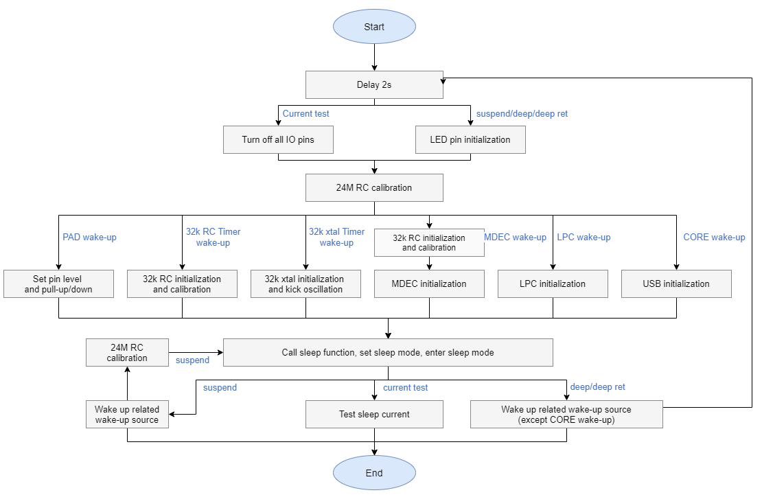
Flowchart explanation:
(1) The 2-second delay at the beginning is added to maintain communication availability. Since the Swire (single-wire debug interface) is unavailable after entering sleep mode, the BDT may fail to activate, preventing firmware programming.
(2) All IO pins are disabled before current measurement to prevent leakage current.
(3) CORE wakeup is supported only in Suspend mode and is not supported in DeepSleep or DeepSleep Retention modes.
(4) In Suspend mode, LED2 is controlled before sleep entry and after wakeup to indicate the current status. In DeepSleep and DeepSleep Retention modes, the chip is powered down during sleep entry, and the LED is automatically turned off. (The LED is only used as a status indicator.)
(5) Since the RC clock has limited accuracy and varies with temperature, periodic calibration is generally required. The following recommendations are provided:
a) 24M RC:
It is recommended to calibrate the RC clock every 10 seconds before entering sleep. The RC clock accuracy affects the crystal oscillator startup time after wakeup. After waking up from sleep, the hardware uses the 24M RC clock to kick-start the crystal oscillator. Higher RC clock accuracy results in a shorter crystal oscillator startup time.
b) 32K RC:
The RC clock is calibrated once during power-on and once after exiting DeepSleep. Since PM uses the tracing method (using the 16M clock to measure the fixed period of the 32K clock), the RC clock accuracy does not affect the Timer wakeup timing accuracy.
If other modules use the 32K RC clock, corresponding handling is required based on application requirements.
c) 32K xtal:
It needs to be re-kicked after power-on. When using the 32K XTAL, external capacitors need to be soldered on the board.
Watchdog
Overview
Watchdog is an important mechanism in MCU systems used to detect and recover from software anomalies. When software cannot run normally due to issues such as infinite loops or deadlocks, the watchdog timer overflow triggers a system reset, allowing the chip to return to normal operation.
The Telink platform supports the following two types of Watchdogs:
-
Timer Watchdog (regular watchdog): A digital watchdog based on a system timer, operating in active mode, with a clock source of pclk. After overflow, a digital reset is triggered, with the reset range the same as software reboot. Most chips support this feature. See the table below for details.
-
32k Watchdog: A watchdog based on a 32K clock source, it can operate in active/suspend/deep retention modes, and triggers a reset effect similar to power-on after overflow. Enabled by default after hardware power-on, it continues operating during sleep. Some chips support this feature. See the table below for details.
Chip difference description
Watchdog feature differences summary
| Chip model | Timer Watchdog | 32k Watchdog |
|---|---|---|
| B80 | √ | √ |
| B80B | √ | √ |
| B85 | √ | ✗ |
| B87 | √ | ✗ |
| TC321x | √ | √ |
| TC1211 | X | √ |
| TC122x | ✗ | √ |
| B91 | √ | ✗ |
| B92 | √ | √ |
| TL321x | √ | √ |
| TL322x | √ | √ |
| TL323x | √ | √ |
| TL721x | √ | √ |
| TL751x | √ | √ |
Standard Watchdog (Timer Watchdog)
TL series code description
Timer Watchdog is based on the pclk clock source and operates only in active mode. Taking the TL series as an example, the following interfaces are defined in watchdog.h and watchdog.c.
Interface list:
| Interface | Function |
|---|---|
wd_start() |
Enable the watchdog |
wd_stop() |
Disable the watchdog |
wd_set_interval_ms(period_ms) |
Set watchdog trigger time (unit: ms) |
wd_clear() |
Feed the watchdog to clear the watchdog timer counter. |
wd_get_status() |
Obtain the watchdog overflow status |
wd_clear_status() |
Clear the watchdog overflow status flag |
TC series code description
Timer Watchdog is based on the system clock source and operates only in active mode, using timer2, which can act as both a watchdog and a regular timer. Taking the TC series as an example, the following interfaces are defined in watchdog.h and watchdog.c.
Interface list:
| Interface | Function |
|---|---|
wd_start() |
Enable the watchdog |
wd_stop() |
Disable the watchdog |
wd_set_interval_ms(period_ms, tick_per_ms) |
Set watchdog trigger time (unit: ms) |
wd_clear() |
Feed the watchdog to clear the watchdog timer counter. |
wd_get_status() |
Obtain the watchdog overflow status |
Usage Example
// Initialize and activate the watchdog
wd_set_interval_ms(1000, sys_tick_per_ms);  // Set trigger after 1 s
wd_start();

// Feed the watchdog periodically in the main loop
while (1) {
    wd_clear();
    // user code
}
32k Watchdog
TL series code description
Interface list:
| Interface | Function |
|---|---|
wd_32k_start() |
Enable the 32k watchdog |
wd_32k_stop() |
Disable the 32k watchdog |
wd_32k_set_interval_ms(period_ms) |
Set the trigger time in milliseconds, and the clock automatically selects the appropriate clock mode and calculates the countdown value. |
wd_32k_set_target_value(clk_sel, target) |
The trigger time can be set directly using the divider level and counter value, which is suitable for scenarios requiring fine-grained control. It is an internal interface called by wd_32k_set_interval_ms() and is not recommended for users. Actual trigger time = Divider single-period width × Counter value |
wd_32k_feed() |
Feed the dog |
wd_32k_get_count_ms() |
Get the current count value (ms) |
wd_32k_get_status() |
Return to overflow state. After a 32 kHz watchdog reset, the status is set to 1 after reboot. The wd_32k_clear_status() function must be called to clear the status; otherwise, it may affect subsequent status checks. The status is retained after software reset, deep sleep, deep sleep with retention, and 32 kHz watchdog reset. The status is lost after a power cycle, a reset pin reset, and a VBUS detection reset. |
wd_32k_clear_status() |
Clear the overflow status flag |
TC series code description
Interface list:
| Interface | Function |
|---|---|
wd_32k_start() |
Enable the 32k watchdog |
wd_32k_stop() |
Disable the 32k watchdog |
wd_32k_set_interval_ms(period_ms) |
Set the trigger time by ms |
wd_32k_get_status() |
Obtain overflow status |
wd_32k_clear_status() |
Clear the overflow status flag |
32k Watchdog Solutions 1 and 2
| Chip model | 32k Watchdog Solution 1 | 32k Watchdog Solution 2 |
|---|---|---|
| B80 | √ | X |
| B80B | √ | X |
| B85 | X | X |
| B87 | X | X |
| TC321x | √ | X |
| TC1211 | √ | X |
| TC122x | ✗ | √ |
| B91 | X | X |
| B92 | √ | X |
| TL321x | √ | X |
| TL322x | √ | X |
| TL323x | X | √ |
| TL721x | √ | X |
| TL751x | √ | X |
Differences between Solution 1 and Solution 2:
Solution 1:
- Unable to obtain the current 32k watchdog count.
- The watchdog can only be fed by calling
wd_32k_set_interval_ms(period_ms). Before feeding the watchdog, it must be disabled first. After the configuration is completed, enable it again. - When configuring the target value, the watchdog must be disabled first. After the configuration is completed, enable it again. Because the analog register cannot write 4 bytes at a time, only one can be written. During writing, there is concern about uncertain intermediate values, which could lead to an unexpected 32k watchdog reset, so it is closed before writing.
Solution 2:
- The current count value (ms) can be obtained via
wd_32k_get_count_ms(). - The watchdog can be fed directly by calling
wd_32k_feed()without disabling it. - The trigger time can be set using
wd_32k_set_interval_ms(period_ms)without requiring users to perform additional watchdog enable/disable operations.
Configuration precautions:
- If there is no timer as the wake-up source in sleep mode, only pad wake-up is used. Since there is no clock, the 32k watchdog count pauses.
- When using the timer wake-up function, ensure that the watchdog reset time is later than the wake-up time.
- For OTP products, if all code cannot run in RAM, there is a risk of crashes, so the 32K Watchdog needs to be enabled. This interface must be placed in RAM code to reduce risk.
- For chips using Solution 1, when configuring the trigger time, the watchdog must be disabled before configuration, and only enabled after configuration. Using the chip from Solution 2, the
wd_32k_set_interval_mshandle this operation internally and can be called directly. TL321x, although using Solution 1, internally handles this workflow and can also be called directly.
Usage Example:
Solution 1: The watchdog feeding procedure is the same as the reset time configuration procedure.
// Set and start in milliseconds
wd_32k_stop();
wd_32k_set_interval_ms(2000);  // Set 2s trigger
wd_32k_start();

// Feed the dog:
wd_32k_stop();
wd_32k_set_interval_ms(2000);
wd_32k_start();
Solution 2:
// Set and start in milliseconds
wd_32k_set_interval_ms(2000);  // Set 2s trigger
// Feeding the dog:
wd_32k_feed();
FAQ
Q: How can I determine whether the system was reset by the watchdog?
A:Call pm_update_status_info() to obtain the reset reason, and check the pm_status.mcu_status variable to determine whether the system was reset by the watchdog or resumed from another wake-up source. See pm_update_status_info in the Power section for details.
RF
Overview
RF Module Overview
The Telink chip integrates a single RF hardware engine that supports multiple wireless protocols, including BLE, Zigbee, 2.4G Proprietary, and ANT. RF modes can be switched through software. In different application scenarios, the same chip can flexibly switch between protocols such as BLE, Zigbee, and 2.4G Proprietary by simply calling the corresponding mode-switching interface, without requiring any additional hardware modifications.
Chip Supported Modes
Supported modes vary by chip series. The following table lists the modes supported across all chip series. For the exact definitions of each supported mode, refer to the SDK header files for the corresponding chip.
| Protocol Type | Supported Modes | Modulation | Description |
|---|---|---|---|
| BLE | 1M / 2M | GFSK | Standard BLE 1 Mbps / Enhanced 2 Mbps |
| BLE | 500K / 125K (LE Coded) | GFSK | BLE Coded S=2 / S=8 long-range mode |
| Zigbee | 250K | O-QPSK | IEEE 802.15.4 compliant (not supported on all chips) |
| Zigbee | Hybee 1M / 2M / 500K | O-QPSK | Hybee extended mode (supported on some chips) |
| 2.4G Proprietary | 250K / 500K / 1M / 2M | GFSK | Supports TPLL/SB frame format |
| 2.4G Proprietary (Generic) | 250K / 500K / 1M / 2M | GFSK | Proprietary protocol with customizable frame format |
Note
- The TC321x / TC1211 / TC122x / TC123x series chips do not support Zigbee and Hybee modes. The TLSR825x / TLSR827x/ TLSR8208 series and TL series chips support Zigbee and Hybee modes.
Driver File Structure
TL series chips use a modular driver structure:
rf_common.h: Common settings (initialization, frequency, power, fast settle, CRC, etc.)rf_ble.h: BLE mode relatedrf_zigbee.h: Zigbee / Hybee mode relatedrf_private.h: Proprietary mode relatedrf_dma.h: DMA related
TC series chips driver files:
rf_drv.h: RF common APIs and mode setting interfacesrf.h: Low-level RF driver declarations
Wireless Protocol Frame Format
This chapter uses BLE mode as an example to describe the TX/RX frame layout in RAM. For other protocols, only the differences from BLE are listed.
BLE Frame Format (Detailed Example)
Over-the-air (OTA) frame format:
| Field | Preamble | Access Code | PDU | CRC |
|---|---|---|---|---|
| Length | 1 Byte (1M) / 2 Bytes (2M) | 4 Bytes | 2–257 Bytes | 3 Bytes |
- Preamble: 1 byte (0xAA) in 1M mode, 2 bytes in 2M mode
- Access Code: 4 bytes. The advertising Access Code is fixed at 0x8E89BED6
- CRC: CRC-24, polynomial 0x65b, initial value 0x555555
TX Frame Format (RAM Layout):
| RAM Address | Content | Description |
|---|---|---|
| addr, addr + 1 | DMA_LEN_INFO | DMA transfer length, LSB first |
| addr + 2, addr + 3 | DMA_LEN_INFO | DMA transfer length, LSB first |
| addr + 4 | header0 | Refer to the BLE specification |
| addr + 5 | header (payload length) | Payload length, excluding the 3-byte CRC |
| addr + 6 | data(0) | payload |
| ... | ... | payload |
| addr + 6 + (length - 1) | data(length - 1) | payload |
RX Frame Format (RAM Layout):
| RAM Address | Content | Description |
|---|---|---|
| rba, rba + 1 | DMA_LEN_INFO | DMA transfer length, LSB first |
| rba + 2, rba + 3 | DMA_LEN_INFO | DMA transfer length, LSB first |
| rba + 4 | header0 | Refer to the BLE specification |
| rba + 5 | header1 (payload length) | Payload length |
| rba + 6 | data(0) | payload |
| ... | ... | payload |
| rba + 6 + length | crc(0) | CRC byte 0 |
| rba + 6 + length + 1 | crc(1) | CRC byte 1 |
| rba + 6 + length + 2 | crc(2) | CRC byte 2 |
| rba + 6 + length + 3 | r_tstamp[7:0] | Timestamp byte 0 |
| rba + 6 + length + 4 | r_tstamp[15:8] | Timestamp byte 1 |
| rba + 6 + length + 5 | r_tstamp[23:16] | Timestamp byte 2 |
| rba + 6 + length + 6 | r_tstamp[31:24] | Timestamp byte 3 |
| rba + 6 + length + 7 | pkt_fdc[7:0] | Frequency offset low byte |
| rba + 6 + length + 8 | pkt_fdc[10:8] | Frequency offset high byte |
| rba + 6 + length + 9 | pkt_rssi | Packet RSSI |
| rba + 6 + length + 10 | bit[0] | CRC error flag |
| Same | bit[1] | SFD error flag |
| Same | bit[2] | Link layer error flag |
| Same | bit[3] | Power error flag |
| Same | bit[7] | NoACK indicator |
RX Packet Parsing Macros:
| TL Series Macro | TC Series Macro | Description |
|---|---|---|
rf_ble_packet_crc_ok(p) |
RF_BLE_PACKET_CRC_OK |
Check whether RX packet CRC is correct |
rf_ble_packet_length_ok(p) |
RF_BLE_PACKET_LENGTH_OK |
Check whether RX packet length is correct |
rf_ble_dma_rx_offset_rssi(p) |
N/A | Offset of the RSSI value in the packet |
rf_ble_dma_rx_offset_freq_offset(p) |
N/A | Frequency offset info offset in the packet |
rf_ble_dma_rx_offset_time_stamp(p) |
N/A | RX timestamp info offset in the packet |
rf_ble_dma_rx_offset_crc24(p) |
N/A | CRC value offset in the packet |
Note
- The calculation of DMA_LEN_INFO varies by chip series. TL series provides the macro
rf_tx_packet_dma_len(data_len)to calculate the DMA length, with the formula((data_len + 3) / 4) | ((data_len % 4) << 22). TC series directly fills in the actual data transfer length (excluding the DMA_LEN_INFO bytes). For other related macro definitions, refer to the corresponding chip'srf_drv.h/rf.h.
2.4G Proprietary Frame Format — Differences from BLE
Proprietary supports two sub-modes: TPLL (Telink Proprietary Link Layer) and SB (ShockBurst).
OTA frame differences:
| Parameter | BLE | Proprietary TPLL / SB |
|---|---|---|
| Synchronization Word | Access Code (4 bytes fixed) | Configurable 3–5 bytes |
| Preamble | 1–2 bytes | Configurable 1–16 bytes |
| CRC | Fixed CRC-24 | CRC-16 |
RAM Layout Differences:
Compared with the BLE TX frame format:
- TPLL: The payload length is stored at addr + 4 (BLE uses header0), and payload data starts at addr + 5. The DMA_LEN_INFO field structure is the same.
- SB: Payload data starts directly at addr + 4, with no payload length field. A fixed length must be set via
rf_fix_payload_len_set().
Compared with the BLE RX frame format:
The trailing information appended to the RX packet has the same structure as BLE (CRC -> Timestamp -> Frequency Offset -> RSSI -> Error Flags), with only the parsing macros differing by sub-mode:
| TL Series Macro | TC Series Macro | Applicable Mode |
|---|---|---|
rf_pri_tpll_packet_crc_ok(p) |
RF_TPLL_PACKET_CRC_OK(p) |
TPLL mode |
rf_pri_tpll_packet_length_ok(p) |
RF_TPLL_PACKET_LENGTH_OK(p) |
TPLL mode |
rf_pri_sb_packet_crc_ok(p) |
RF_SB_PACKET_CRC_OK(p) |
SB mode |
rf_pri_sb_packet_payload_length_get(p) |
RF_SB_PACKET_PAYLOAD_LENGTH_GET(p) |
SB mode |
Note
- For TL series, other related offset macros can be found in the corresponding header file for each mode. For TC series, related macros can be found in
rf_drv.h/rf.h.
Zigbee Frame Format — Differences from BLE
Note
- Zigbee mode is supported only on some chips. Refer to the corresponding chip's datasheet.
OTA frame differences:
| Parameter | BLE | Zigbee |
|---|---|---|
| Preamble | 1~2 Byte | 4 Bytes |
| Synchronization Identifier | Access Address (4 bytes) | SFD (1 byte, fixed 0xA7, auto-detected by hardware) |
| Frame Header | 2-byte Header | 1-byte PHR (lower 7 bits = PSDU length) |
| CRC | CRC-24 | CRC-16 CCITT (polynomial 0x1021, initial value 0x0000) |
RAM Layout Differences:
Compared with the BLE TX frame format, Zigbee has an additional MAC layer header (Frame Control, Sequence Number, PAN ID, address fields, etc.) at addr + 4 to addr + 12. The payload length is at addr + 13, and payload data starts at addr + 14. Key differences:
- Zigbee / Hybee modes have no access code concept, so no access code configuration is required during initialization.
- SFD (0xA7) is auto-detected by hardware.
Compared with the BLE RX frame format, the trailing information appended to the Zigbee RX packet has the same structure as BLE.
Parsing macros: RF_ZIGBEE_PACKET_CRC_OK(p), RF_ZIGBEE_PACKET_LENGTH_OK(p), RF_ZIGBEE_PACKET_RSSI_GET(p), etc. Usage is the same as the BLE macros.
2.4G Generic Frame Format — Differences from Proprietary
The Generic mode is an extension of the Proprietary mode, offering greater frame format flexibility. In addition to configurable parameters such as CRC length, polynomial, and initial value, it also supports the packet filter feature as needed. For specific usage and details, refer to the relevant code in RF_Demo.
Note
- Generic mode is supported only on some TL series chips. Refer to the corresponding chip's datasheet for details.
RF TX/RX Operating Modes and State Machine
Manual Mode
In Manual mode, all TX and RX processes are controlled by software flow. The hardware performs only basic transmit and receive operations, without automatically managing state transitions, timing, or retransmissions. The timing accuracy in Manual mode depends on the software implementation.
(1) Manual TX
After entering TX mode via rf_set_txmode() and waiting for the settle time (which must be controlled by software in Manual mode), you can call rf_tx_pkt() directly to send a packet. For specific usage, refer to the relevant code in RF_Demo.
Note
- In Manual TX mode, the settle wait is required only once when first entering TX mode. The TX state remains active thereafter.
(2) Manual RX
After entering RX mode via rf_set_rxmode() and waiting for the settle time (which must be controlled by software in Manual mode), the device enters the actual receive state. In this mode, packets can be received continuously.
Note
- In Manual RX mode, the settle wait is required only once when first entering RX mode. After receiving one packet, the device directly enters the next receive state.
Auto Mode
Unlike Manual mode, Auto mode triggers the state machine at a specified time via a trigger tick. The hardware state machine automatically completes the entire Settle -> TX/RX -> IDLE sequence without MCU intervention.
The following six core state machine modes are supported:
| No. | Mode | Description | Trigger API |
|---|---|---|---|
| 1 | STX | Single transmission. Enters TX settle after triggering, returns to IDLE automatically after sending. | rf_start_stx(addr, tick) |
| 2 | SRX | Single reception. Enters RX settle after triggering, returns to IDLE automatically after receiving or timeout. | rf_start_srx(tick) |
| 3 | PTX | Periodic transmission with auto-retransmission and ACK reception. | rf_start_ptx(addr, tick) |
| 4 | PRX | Periodic reception. Automatically replies with ACK after receiving data. | rf_start_prx(addr, tick) |
| 5 | TX2RX | Transmit then receive. Sends a packet then waits to enter RX; exits on timeout. | rf_start_stx2rx(addr, tick) |
| 6 | RX2TX | Receive then transmit. Receives data then waits and replies with a packet; exits directly on timeout. | rf_start_srx2tx(addr, tick) |
(1) Trigger Tick Description
The tick parameter of each Auto mode specifies the time point at which the hardware triggers the operation. When the current system timer value ≥ tick, the hardware automatically triggers the corresponding state machine operation. The trigger time is obtained by adding an appropriate delay to the current system timer value.
// tick calculation: rf_start_xxx(packet, system_tick + delay_ticks)
// delay_ticks = delay in milliseconds × system timer ticks per millisecond
Note
- The tick parameter takes effect only when the current timer value is less than the tick value. When the timer value reaches or exceeds the tick value, the hardware triggers immediately.
(2) STX — Single Transmission
void rf_start_stx(void *addr, unsigned int tick)
| Parameter | Description |
|---|---|
| addr | TX packet address, must be 4-byte aligned |
| tick | Trigger tick value, triggers immediately when reached |
State machine flow:
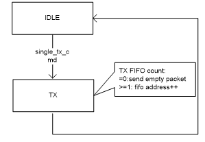
The STX hardware flow is: reach tick time -> TX Settle -> send packet -> return to IDLE automatically. Each call to rf_start_stx triggers one complete transmission sequence.
// Typical interrupt handling flow:
Interrupt triggered (FLD_RF_IRQ_TX / FLD_RF_IRQ_CMD_DONE) ->
    Clear interrupt flag ->
    Load next packet data ->
    rf_start_stx(next_packet, trigger_tick)   // Schedule next transmission
(3) SRX — Single Reception
void rf_start_srx(unsigned int tick)
| Parameter | Description |
|---|---|
| tick | Trigger tick value |
State machine flow:
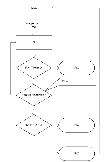
The SRX hardware flow is: reach tick time -> RX Settle -> wait for sync word (Sync Word / Access Address) -> upon successful sync, receive the complete packet and perform CRC check -> return to IDLE automatically.
(4) TX2RX — Transmit Then Receive
void rf_start_stx2rx(void *addr, unsigned int tick)
| Parameter | Description |
|---|---|
| addr | TX packet address, 4-byte aligned |
| tick | Trigger tick value |
State machine flow:
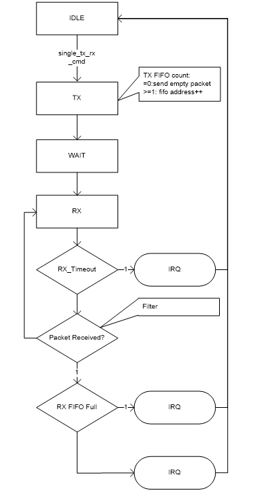
TX2RX is a bidirectional single-shot state machine. The hardware flow is: reach tick time -> TX Settle -> send packet -> TX done -> RX Wait -> auto-switch to RX Settle -> wait for the peer's reply packet or timeout -> return to IDLE automatically.
(5) RX2TX — Receive Then Transmit
void rf_start_srx2tx(void *addr, unsigned int tick)
| Parameter | Description |
|---|---|
| addr | Reply packet address, 4-byte aligned |
| tick | Trigger tick value |
State machine flow:
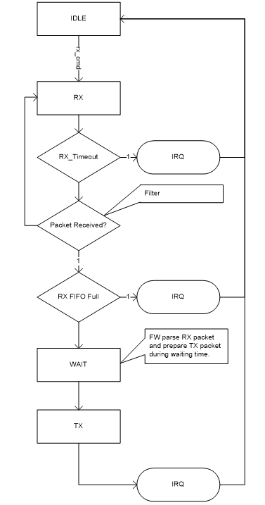
RX2TX is the complementary mode of TX2RX. The hardware flow is: reach tick time -> RX Settle -> wait for sync word -> receive packet -> RX done or timeout -> return to IDLE -> TX Wait -> auto-switch to TX Settle -> send reply packet -> return to IDLE automatically.
(6) PTX — Periodic Transmission
void rf_start_ptx(unsigned char *addr, unsigned int tick)
| Parameter | Description |
|---|---|
| addr | TX packet address, 4-byte aligned |
| tick | Trigger tick value |
PTX configuration interfaces:
| Interface | Description |
|---|---|
rf_ptx_prx_config() |
Initializes PTX / PRX mode configuration |
rf_set_ptx_prx_ack_en() |
Enables ACK |
rf_set_ptx_prx_ack_dis() |
Disables ACK |
rf_set_ptx_retry(retry_count, retry_delay) |
Sets retry count and retry delay |
In PTX mode, the hardware automatically handles all transaction processing, including packet assembly (Preamble + Access Code + Header + Payload + CRC), ACK reception, and auto-retransmission, without MCU involvement. A complete transaction is defined as: PTX sends a data packet -> receives an ACK packet from PRX.
PID (Packet Identification) Mechanism:
Each time PTX sends a new data packet, the PID field increments by 1 (2-bit, range 0–3). PRX uses the PID + CRC combination to determine whether a received packet is new or a retransmission, thereby avoiding duplicate delivery to the application layer. Even when the CRC is the same, the PID helps distinguish them.
Retry Delay (retry_delay) Description:
The retry_delay in rf_set_ptx_retry(retry_count, retry_delay) is defined as the interval between the start times of two transmissions, rather than the interval from the end of the previous transmission to the start of the next.
PTX State Machine Flow:
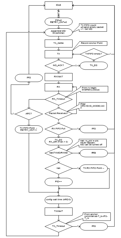
In PTX mode, after sending a data packet, the transmitter automatically switches to RX mode to wait for an ACK response from the receiver. If no valid ACK is received within the specified time (CRC check failure or timeout), the transmitter automatically retransmits according to the configured retry count (rf_set_ptx_retry). When the retry count exceeds the configured value, the FLD_RF_IRQ_TX_RETRYCNT interrupt is triggered, and the transmitter returns to IDLE. PTX supports PRX sending data (payload) in the ACK packet, in which case the PTX side triggers the FLD_RF_IRQ_RX_DR interrupt to notify the MCU to read the data.
Note
- PTX / PRX interface names may vary slightly across chip series. Some TL series chips use
rf_ptx_config()/rf_prx_config()for separate initialization, andrf_start_ptxmay have a different parameter signature (accepting only the tick parameter). Refer to the specific chip's SDK header file for details.
(7) PRX — Periodic Reception
void rf_start_prx(unsigned char *addr, unsigned int tick)
| Parameter | Description |
|---|---|
| addr | RX data storage address, 4-byte aligned |
| tick | Trigger tick value |
After receiving data, an ACK is automatically replied. As the primary receiver, PRX only automatically responds with an ACK upon receiving a valid data packet from PTX.
PRX PID Duplicate Detection Mechanism:
PRX uses the PID + CRC combination to determine whether the currently received packet is a retransmission. If the PID is the same as the last successfully received packet and the CRC also matches, the packet is identified as a duplicate — it will be discarded (not reported to the application layer), but PRX still automatically replies with an ACK (because PTX may be retransmitting due to a lost ACK).
PRX TX FIFO (ACK Payload):
Before receiving a data packet, PRX can preload data to be sent back into the TX FIFO. When a PTX data packet is received, the hardware automatically sends the data in the TX FIFO as the ACK payload. If the TX FIFO is empty, an empty ACK is sent (containing only Preamble + Access Code + Header/PID + CRC, with no payload).
NO_ACK Flag Handling:
When the NO_ACK flag bit in the received data packet is 1, PRX does not send an ACK packet (in this case, PTX will continue retransmitting until the maximum retry count is reached).
PRX State Machine Flow:
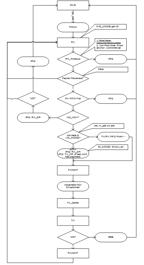
In PRX mode, the receiver continuously monitors the specified channel. When a valid data packet is received (CRC check passed and PID is a new packet), the payload is stored in the RX buffer and reported to the application layer; the receiver then automatically switches to TX mode to reply with an ACK. If there is preloaded data in the RX FIFO, the ACK packet carries that data as well. If no valid sync word is received within the specified time, the FLD_RF_IRQ_RX_TIMEOUT interrupt is triggered, and the receiver returns to IDLE (in periodic monitoring mode, it re-enters RX Settle at the next tick).
RF Interrupt System
Common Interrupts Overview
| Interrupt Name | Code Bit Name | Trigger Mode | Trigger Principle and Mechanism |
|---|---|---|---|
| TX Interrupt | FLD_RF_IRQ_TX | Manual TX / STX / PTX / RX2TX / TX2RX | Generated immediately after each packet is sent |
| RX Interrupt | FLD_RF_IRQ_RX | Manual RX / SRX / PRX / TX2RX / RX2TX | Generated after each packet is received and CRC check passes |
| RX Timeout Interrupt | FLD_RF_IRQ_RX_TIMEOUT | SRX / PRX / TX2RX | Generated when no sync word is received within the RX window, upon timeout |
| First RX Timeout Interrupt | FLD_RF_IRQ_FIRST_RX_TIMEOUT | SRX / PRX / RX2TX | Generated upon the first RX timeout (the first timeout after entering RX) |
| RX CRC Error Interrupt | FLD_RF_IRQ_RX_CRC_2 | BTX / BRX / PTX / PRX | Generated when two consecutive CRC errors are detected |
| TX DS Interrupt | FLD_RF_IRQ_TX_DS | PTX / PRX | Generated when the transmitted payload length is not 0 |
| RX DR Interrupt | FLD_RF_IRQ_RX_DR | PRX / PTX / SRX | Generated when the received packet payload length is not 0 |
| Invalid PID Interrupt | FLD_RF_IRQ_INVALID_PID | PTX / PRX | Generated when an invalid PID is received |
Core Interrupt Low-Level Functional Analysis
The interrupt operation interfaces vary by chip series, as listed below.
TL Series:
| Interface | Description |
|---|---|
rf_get_irq_status(status) |
Gets the status of the specified interrupt flag (read reg_rf_irq_status) |
rf_clr_irq_status(status) |
Clears the specified interrupt flag (write 1 to clear) |
rf_set_irq_mask(mask) |
Sets the interrupt mask (reg_rf_irq_mask) |
rf_clr_irq_mask(mask) |
Clears the interrupt mask |
TC Series:
| Interface | Description |
|---|---|
rf_irq_src_get() |
Gets the current RF interrupt source status (read reg_rf_irq_status) |
rf_irq_clr_src(msk) |
Clears the specified RF interrupt source (write 1 to clear) |
rf_irq_enable(msk) |
Enables the specified RF interrupt |
rf_irq_disable(msk) |
Disables the specified RF interrupt |
ISR Best Practice (refer to rf_irq_handler in app_ble_mode.c):
TL Series:
void rf_irq_handler(void)
{
    // 1. Read interrupt status
    unsigned int irq_status = rf_get_irq_status();

    // 2. Clear interrupt flags
    rf_clr_irq_status(irq_status);

    // Dispatch by interrupt type
    if (irq_status & FLD_RF_IRQ_TX) {
        // Handle TX completion
    }
    if (irq_status & FLD_RF_IRQ_RX) {
        // Handle RX completion
    }
    if (irq_status & FLD_RF_IRQ_RX_TIMEOUT) {
        // Handle RX timeout
    }
}
TC Series:
void irq_handler(void)
{
    // 1. Read interrupt status
    unsigned int irq_status = rf_irq_src_get();

    // 2. Clear interrupt flags
    rf_irq_clr_src(irq_status);

    // Dispatch by interrupt type
    if (irq_status & FLD_RF_IRQ_TX) {
        // Handle TX completion
    }
    if (irq_status & FLD_RF_IRQ_RX) {
        // Handle RX completion
    }
    if (irq_status & FLD_RF_IRQ_RX_TIMEOUT) {
        // Handle RX timeout
    }
}
RF DMA
RF Dedicated DMA Channels
RF TX/RX data transfer is performed through dedicated DMA channels:
| DMA Channel | Function |
|---|---|
| RF_TX_DMA (Ch0) | RF TX DMA channel, reads data from RAM and sends it to the RF hardware FIFO |
| RF_RX_DMA (Ch1) | RF RX DMA channel, receives data from the RF hardware FIFO and writes it to RAM |
TX DMA Configuration
The first two bytes of the TX buffer are DMA_LEN_INFO, indicating the data length to be transferred by DMA. The calculation of DMA_LEN_INFO varies by chip series:
- TL Series: Provides macro
rf_tx_packet_dma_len(rf_data_len)with formula((rf_data_len + 3) / 4) | ((rf_data_len % 4) << 22) - TC Series: Directly fill in the actual data transfer length (excluding the DMA_LEN_INFO bytes), LSB first
RX DMA Configuration
TL Series:
void rf_set_rx_dma(unsigned char *buff, unsigned char fifo_num, unsigned short fifo_byte_size)
| Parameter | Description |
|---|---|
| buff | RX buffer address, must be 4-byte aligned |
| fifo_num | RX FIFO count (total number of RX FIFOs minus 1) |
| fifo_byte_size | Depth of each FIFO in bytes, must be a multiple of 16 |
TL Series also provides TX DMA configuration interfaces:
void rf_set_tx_dma(unsigned char fifo_depth, unsigned short fifo_byte_size)
- fifo_depth: FIFO depth information. FIFO count = 2^fifo_depth.
- fifo_byte_size: Size of a single FIFO, in bytes.
TC Series:
void rf_rx_buffer_set(unsigned char *RF_RxAddr, int size, unsigned char PingpongEn)
| Parameter | Description |
|---|---|
| RF_RxAddr | RX buffer address, must be 4-byte aligned |
| size | RX buffer size, must be a multiple of 16 |
| PingpongEn | Ping-Pong buffer enable: 1 = enabled, 0 = disabled |
- When PingpongEn = 0: received data is stored in a single buffer pointed to by RF_RxAddr
- When PingpongEn = 1: received data is stored alternately in buffer0 and buffer1, the reserved RAM size should be size * 2
DMA Usage Notes
- DMA Configuration Timing Requirement: DMA-related configurations (
rf_rx_buffer_set/rf_set_rx_dma, etc.) must be completed before the RF state machine starts. The DMA must be configured before the RF state machine. - TX DMA Pre-fill and RF STX Start Timing Coordination: Before calling functions such as
rf_start_stx/rf_start_ptx, the TX buffer data must be ready. - RX DMA Ring Buffer and FIFO Overflow Timing Protection: The total amount of received data must not exceed the buffer size; otherwise, FIFO overflow will cause data loss.
- Buffer Must Be 4-Byte Aligned: TX / RX buffers must be 4-byte aligned. Use
__attribute__ ((aligned (4)))to declare them.
RF General Configuration
RF General Hardware Configuration
(1) rf_mode_init()
RF module initialization is the first step in using RF functionality. The TC series and TL series have differences, as described below:
- TL Series & New TC Series: First call
rf_mode_init()to complete basic initialization, then call the specific mode setting function. - TLSR825x / TLSR827x Series: Use
rf_drv_init(RF_ModeTypeDef)to complete initialization and mode selection in a single step.
Note
rf_mode_init()orrf_drv_init()must be called first, and only once during the system initialization phase.
(2) Modulation and OTA Data Rate Low-Level Configuration
| Protocol | TL Series API | TC Series API | Description |
|---|---|---|---|
| BLE 1M | rf_set_ble_1M_mode() |
rf_set_ble_1M_mode() |
Standard BLE 1 Mbps |
| BLE 2M | rf_set_ble_2M_mode() |
rf_set_ble_2M_mode() |
High-speed BLE 2 Mbps |
| BLE 500K | rf_set_ble_500K_mode() |
rf_set_ble_500K_mode() |
BLE Coded S=2 |
| BLE 125K | rf_set_ble_125K_mode() |
rf_set_ble_125K_mode() |
BLE Coded S=8 |
| Zigbee | rf_set_zigbee_250K_mode() |
rf_set_zigbee_250K_mode() |
250Kbps Zigbee O-QPSK |
| Proprietary | rf_set_pri_250K_mode(), etc. |
rf_set_pri_250K_mode(), etc. |
Selectable rate: 250K/500K/1M/2M bps |
Note
- TLSR825x / TLSR827x series chips complete mode selection in a single step via
rf_drv_init(RF_MODE_xxx). For example,rf_drv_init(RF_MODE_BLE_1M)sets the BLE 1M mode, andrf_drv_init(RF_MODE_ZIGBEE_250K)sets the Zigbee mode.
(3) Channel
BLE Channel Setting (recommended for BLE mode):
void rf_set_ble_chn(signed char chn_num)
Frequency mapping formula: f = 2402 + channel (MHz). The parameter chn_num is mapped according to the BLE specification; for example, chn_num = 37 -> 2402 MHz.
General Channel Setting (applicable to all modes):
TL series:
void rf_set_chn(signed char chn)
| Parameter | Description |
|---|---|
| chn | Channel index, actual frequency = 2400 + chn, range 2–80 |
TC series:
void rf_set_chn(signed char chn, unsigned short set)
| Parameter | Description |
|---|---|
| chn | Channel index, actual frequency = 2400 + chn, range 2–80 |
| set | Internal channel setting value, typically pass 0 |
Note
rf_set_chnis applicable to all modes;rf_set_ble_chnis applicable only to BLE mode.
(4) Power
Differences Between VBAT and VANT Power Supply Modes:
- VBAT Mode: The RF PA module is powered directly by the battery (VBAT). It supports a wide output power range, including high-power levels such as +10 dBm, but the actual output power decreases as the battery voltage drops.
- VANT Mode: The RF PA module is powered by an internal LDO regulator. The output power is stable (independent of battery voltage), making it suitable for low-power scenarios, but the maximum power level is lower.
Power setting interfaces:
void rf_set_power_level(RF_PowerTypeDef level)
void rf_set_power_level_index(RF_PowerTypeDef level)
The two are functionally equivalent, differing only in the enumeration type, and can be chosen as needed.
Note
- Different chips support different maximum transmit power levels. Refer to the
rf_drv.horrf_common.hheader file of the corresponding chip's SDK for the specific power enumeration values. The actual transmit power is affected by factors such as antenna matching and PCB routing, and hardware calibration is required during mass production.
(5) CRC
rf_crc_config_t hardware fields:
| Field | Description |
|---|---|
| init_value | CRC initial value |
| poly | Polynomial (BLE: 0x65b, Zigbee: 0x1021) |
| xor_out | Output XOR mask |
| byte_order | MSB First / LSB First |
| start_cal_pos | Start byte position for calculation |
| len | CRC length (0–4 bytes, 0 = disabled) |
Quick reference for default CRC configurations by protocol:
| Protocol | Polynomial | Length | Initial Value | Description |
|---|---|---|---|---|
| BLE 1M / 2M | 0x65b | 3 Bytes | 0x555555 | CRC-24 |
| BLE Coded | 0x65b | 3 Bytes | 0x555555 | CRC-24 |
| Zigbee | 0x1021 | 2 Bytes | 0x0000 | CRC-16 |
| Proprietary | 0x1021 | 2 Bytes | 0xffffffff | CRC-16 |
| Generic | User-configurable | 1–4 Bytes | User-configurable | Flexible configuration |
Note
- The CRC configuration is pre-configured at the driver layer by default. If custom configuration is needed, it must be configured according to the requirements of the specific protocol. Some chips do not support customization; refer to the corresponding chip's SDK documentation for details.
(6) Access Code
| Interface | Description |
|---|---|
rf_acc_code_set(pipe_id, addr) |
Sets the access code for the specified pipe |
rf_access_code_comm(acc) |
Sets the common access code (32-bit integer value) |
Note
- Zigbee mode has no access code concept. Its SFD is auto-detected by hardware and requires no software configuration.
(7) TX / RX Wait
In Auto mode, the wait time must be configured when switching between TX and RX:
void rf_set_rx_wait_time(unsigned short rx_wait_us)   // TX -> RX switching wait time, in µs
void rf_set_tx_wait_time(unsigned short tx_wait_us)   // RX -> TX switching wait time, in µs
These two interfaces configure the intermediate wait time when the state machine switches from TX to RX or RX to TX, ensuring sufficient transition time for the hardware.
Settle Hardware Timing Low-Level Configuration
(1) Settle Hardware Timing Definition and Low-Level Role
- TX Settle (TX_EN -> Before PA Ramp): Includes the PLL frequency locking + LDO stabilization + DAC settling phase. During this phase, the RF hardware completes frequency locking and transmit chain calibration to ensure transmit signal quality.
- RX Settle (RX_EN -> Before AGC Lock): Includes the PLL frequency locking + LDO stabilization + ADC settling phase. During this phase, the RF hardware completes frequency locking and receive chain calibration to ensure receive sensitivity.
Timing diagram:
graph LR
    %% TX Settle
    subgraph TX_Time [◄───────── TX Settle Time ──────────►]
        direction LR
        T1[TX_EN] --> T2[TX Settle]
        T2 --> T3[PA Ramp]
    end
    T3 ==> T4((PA output))

    %% RX Settle
    subgraph RX_Time [◄───────── RX Settle Time ──────────►]
        direction LR
        R1[RX_EN] --> R2[RX Settle]
        R2 --> R3[sync status]
    end
    R3 ==> R4((Start receiving))

    %% Style
    classDef default fill:#f4f6f9,stroke:#34495e,stroke-width:2px,color:#2c3e50;
    classDef action fill:#e1f5fe,stroke:#03a9f4,stroke-width:2px;
    classDef result fill:#e8f5e9,stroke:#4caf50,stroke-width:2px;

    class T1,T2,T3,R1,R2,R3 action;
    class T4,R4 result;
In Manual mode, the software must control the settle wait on its own. In Auto mode, the hardware state machine automatically completes the settle wait.
(2) Low-Level Configuration Interfaces
void rf_set_tx_settle_time(unsigned short tx_stl_us)    // TX settle time, in µs
void rf_set_rx_settle_time(unsigned short rx_stl_us)    // RX settle time, in µs
| Parameter | Default Value | Minimum Value | Maximum Value |
|---|---|---|---|
| TX Settle | 150us | 113us | 0xfff us |
| RX Settle | 150us | 85us | 0xfff us |
Note
- The minimum values listed here apply to most chip models. Some chips may have different minimum values. Refer to the Demo or driver comments for details.
Fast Settle
Fast Settle shortens the settle time by skipping some hardware calibration steps, thereby reducing power consumption and increasing TX/RX switching speed. The specific fast settle time options, enumeration definitions, and interfaces vary by chip series.
Note
- Fast Settle may differ across chips. Refer to the corresponding chip's driver comments for the specific fast settle time.
- Refer to the RF Demo for fast settle usage.
RF Module Low-Level Initialization
Refer to the RF Demo code for the RF module initialization flow as follows.
TL Series Initialization
graph TD
    %% Node
    Start(["System power-on / wake-up"])
    Init["rf_mode_init()<br/>(RF RF basic initialization (once only))"]
    Mode["Mode setting API<br/>(e.g. rf_set_ble_1M_mode())"]

    Power["Power config<br/>rf_set_power_level()"]
    Access["Access Code<br/>rf_access_code_comm()"]
    Channel["Channel config<br/>rf_set_ble_chn()"]

    DMA["DMA config<br/>rf_set_tx_dma()<br/>rf_set_rx_dma()"]
    Optional["Optional config<br/>rf_set_tx_settle_time() /<br/>Fast Settle / PTA 等"]
    End(["Start TX/RX<br/>(Auto / Manual Mode)"])

    %% Connection
    Start --> Init
    Init --> Mode

    %% Parallel branches
    Mode --> Power
    Mode --> Access
    Mode --> Channel

    %% Branch convergence
    Power --> DMA
    Access --> DMA
    Channel --> DMA

    %% Following process
    DMA --> Optional
    Optional --> End

    %% Styling
    classDef default fill:#f8f9fa,stroke:#6c757d,stroke-width:2px,color:#212529;
    classDef start_end fill:#e3f2fd,stroke:#2196f3,stroke-width:2px,color:#0d47a1;
    classDef func fill:#e8f5e9,stroke:#4caf50,stroke-width:2px,color:#1b5e20;

    class Start,End start_end;
    class Init,Mode,Power,Access,Channel,DMA,Optional func;
TL series initialization flow pseudocode (BLE 1M mode):
// Step 1: RF basic initialization (call once only)
rf_mode_init();

// Step 2: Set the communication protocol mode
rf_set_ble_1M_mode();

// Step 3: Configure transmit power
rf_set_power_level_index(target_power_level);

// Step 4: Set access code
rf_access_code_comm(access_code_value);

// Step 5: Configure DMA
rf_set_tx_dma(fifo_depth, fifo_size);        // TX DMA FIFO configuration
rf_set_rx_dma(rx_buff, rx_fifo_num,          // RX DMA FIFO configuration
              fifo_byte_size);

// Step 6: Set channel
rf_set_ble_chn(channel_number);
TC Series Initialization
TC New Series:
graph TD
    %% Node
    Start(["System power-on / wake-up"])
    Init["rf_mode_init()<br/>(RF basic initialization (once only))"]
    Mode["Mode setting API<br/>(e.g. rf_set_ble_1M_mode())"]

    Power["Power config<br/>rf_set_power_level_index()"]
    Access["Access Code<br/>rf_access_code_comm()"]
    Channel["Channel config<br/>rf_set_ble_channel()"]

    DMA["DMA config<br/>rf_rx_buffer_set()"]
    Optional["Optional config<br/>rf_set_tx_settle_time() /<br/>Fast Settle / PTA etc."]
    End(["Start TX/RX<br/>(Auto / Manual Mode)"])

    %% Connection
    Start --> Init
    Init --> Mode

    %% Parallel branches
    Mode --> Power
    Mode --> Access
    Mode --> Channel

    %% Branch convergence
    Power --> DMA
    Access --> DMA
    Channel --> DMA

    %% Following process
    DMA --> Optional
    Optional --> End

    %% Styling
    classDef default fill:#f8f9fa,stroke:#6c757d,stroke-width:2px,color:#212529;
    classDef start_end fill:#e3f2fd,stroke:#2196f3,stroke-width:2px,color:#0d47a1;
    classDef func fill:#e8f5e9,stroke:#4caf50,stroke-width:2px,color:#1b5e20;

    class Start,End start_end;
    class Init,Mode,Power,Access,Channel,DMA,Optional func;
TC new series initialization flow pseudocode (BLE 1M mode):
// Step 1: RF basic initialization (call once only)
rf_mode_init();

// Step 2: Set the communication protocol mode
rf_set_ble_1M_mode();

// Step 3: Configure transmit power
rf_set_power_level_index(target_power_level);

// Step 4: Set access code
rf_access_code_comm(access_code_value);

// Step 5: Set channel
rf_set_ble_channel(channel_number);

// Step 6: Configure DMA
rf_rx_buffer_set(rx_buff, buff_size, pingpong_en);

// Step 7: Optional configuration
rf_set_tx_settle_time(tx_settle_us);        // TX Settle time
rf_set_rx_settle_time(rx_settle_us);        // RX Settle time
TLSR825x/TLSR827x Series:
graph TD
    %% Node
    Start(["System power-on / wake-up"])

    Init["rf_drv_init(mode)<br/>(RF init + mode selection)<br/>e.g. rf_drv_init(RF_MODE_BLE_1M)<br/>((call once only))"]

    Power["Power config<br/>rf_set_power_level_index()"]
    Access["Access Code<br/>rf_access_code_comm()"]
    Channel["Channel config<br/>rf_set_ble_channel()"]

    DMA["DMA config<br/>rf_rx_buffer_set()"]

    End(["Start TX/RX<br/>(Auto / Manual Mode)"])

    %% Connection
    Start --> Init

    %% Parallel branches
    Init --> Power
    Init --> Access
    Init --> Channel

    %% Branch convergence
    Power --> DMA
    Access --> DMA
    Channel --> DMA

    %% Following process
    DMA --> End

    %% Styling
    classDef default fill:#f8f9fa,stroke:#6c757d,stroke-width:2px,color:#212529;
    classDef start_end fill:#e3f2fd,stroke:#2196f3,stroke-width:2px,color:#0d47a1;
    classDef func fill:#e8f5e9,stroke:#4caf50,stroke-width:2px,color:#1b5e20;

    class Start,End start_end;
    class Init,Power,Access,Channel,DMA func;
TLSR825x/TLSR827x Series initialization flow pseudocode:
// Step 1: RF init + mode selection (single step, call once only)
rf_drv_init(RF_MODE_BLE_1M);

// Step 2: Configure transmit power
rf_set_power_level_index(target_power_level);

// Step 3: Set access code
rf_access_code_comm(access_code_value);

// Step 4: Set channel
rf_set_ble_channel(channel_number);

// Step 5: Configure DMA
rf_rx_buffer_set(rx_buff, buff_size, pingpong_en);
RF PHY Test
Overview
What Is RF PHY Test
BQB (Bluetooth Qualification Body) certification is a mandatory qualification test that Bluetooth products must pass before being launched to the market. The Bluetooth Special Interest Group (Bluetooth SIG) requires all products using Bluetooth technology to pass BQB certification to ensure compliance with Bluetooth Core Specifications and interoperability between devices from different manufacturers.
RF PHY Test mainly verifies whether the RF physical layer (RF-PHY) performance of Bluetooth devices meets the requirements defined in the Bluetooth specifications. The test covers two major categories: transmitter (TX) and receiver (RX) performance.
Transmitter (TX) Test Items:
- Output Power
- Modulation Characteristics
- Carrier Frequency Offset and Drift
- In-band Spurious Emissions
Receiver (RX) Test Items:
- Sensitivity
- C/I Performance
- Blocking Performance
- Intermodulation Performance
- PER Report Integrity
Telink PHY Test Solution
The Telink chip PHY Test program supports two usage modes:
| Usage Mode | Description | Application Scenario |
|---|---|---|
| Direct UART Connection to Test Equipment | The chip communicates directly with Bluetooth test equipment (such as CMW500) through a 2-wire UART interface and follows the standard Bluetooth test protocol. | Formal qualification testing |
| BQB_Tool | BQB_Tool is integrated into Telink's BDT (Burning and Debugging Tool). It allows configuration parameters to be modified and provides basic functional verification. | Development debugging and pre-test verification |
Note
- Some TC series chips currently do not support the BQB function in BDT_Tool. Support for these chips will be added gradually in future releases.
PHY Test supports two command interaction methods:
| Command Interface | Description | Driver Support |
|---|---|---|
| 2-Wire | Communicates directly with test equipment through the UART interface and uses the standard Bluetooth test protocol. | Supported (default mode of the current driver) |
| HCI | Communicates with test equipment through the Host Controller Interface (HCI) protocol. HCI Commands are sent by the Host. | Not supported currently. Users can refer to the HCI implementation in the Telink BLE SDK for porting. |
Note
- The PHY Test driver currently supports communication with test equipment only through the 2-Wire UART interface. If the default UART configuration (such as baud rate and TX/RX pins) is used, the device can be connected to the test equipment directly. If users need to modify configuration parameters (such as UART pins, Access Code, or PA control), the configuration can be performed through BQB_Tool.
Chip and SDK Mapping
| Chip Series | SDK Path |
|---|---|
| TL Series | tl_platform_src\demo\vendor\RF_Certification\BQB_Demo |
| TC Series | tc_platform_src\demo\vendor\BQB_EMI_Demo |
BQB_Tool Introduction
Tool Overview
BQB_Tool is a configuration and validation tool integrated into BDT (Burning and Debugging Tool). Its main functions include:
- Configuration Modification: Modify configuration parameters of the BQB test program.
- Basic Function Validation: Simulate the instruction interaction between the test instrument and the chip to verify whether the chip PHY Test function works properly.
Working Principle
The PHY Test program communicates with test instruments (such as CMW500) through the 2-Wire UART interface and follows the standard test protocol defined by the Bluetooth specification. The communication process is shown below:
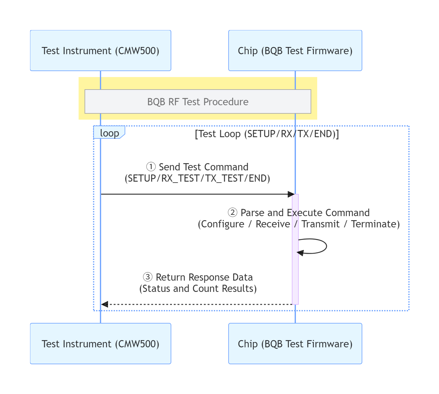
BQB_Tool can be used without an actual test instrument to:
- Modify configuration parameters in the chip firmware (UART pins, power, PA, etc.).
- Simulate test commands and verify whether the chip responds correctly.
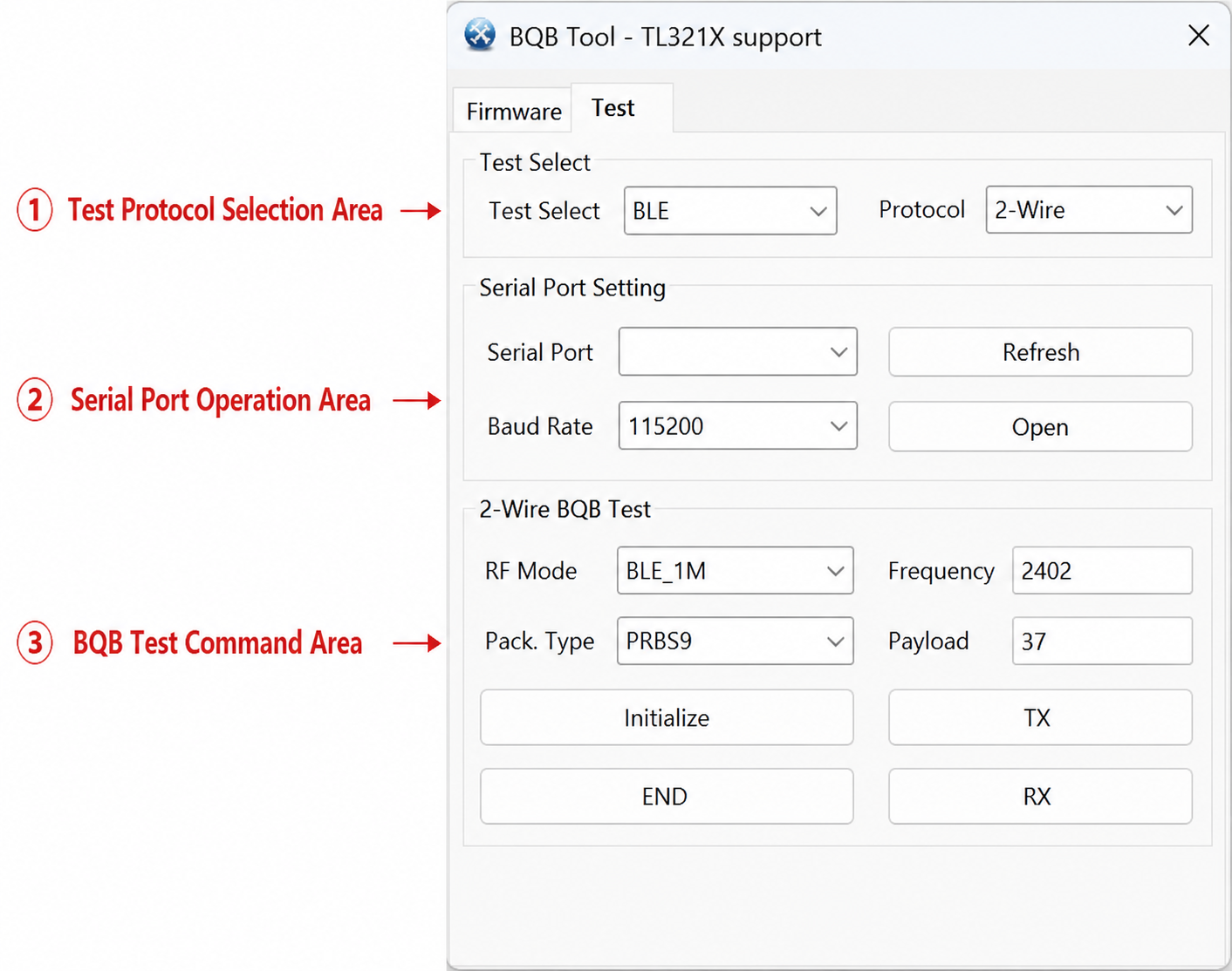
Supported Configuration Items
BQB_Tool supports modification of the following configuration items:
| Configuration Item | Description | Default Value |
|---|---|---|
| UART Baud Rate | UART communication baud rate | 115200 |
| TX Pin | UART transmit pin | Depends on chip model |
| RX Pin | UART receive pin | Depends on chip model |
| Access Code | BLE access address | 0x29417671 |
| TX Power | Transmit power level | Depends on chip model |
| PA TX Pin | External PA transmit control pin | GPIO_PA0 |
| PA RX Pin | External PA receive control pin | GPIO_PA0 |
| Chip Power Supply Mode | LDO/DCDC power supply mode selection | Depends on chip model |
| Internal Capacitor | Whether to enable the internal capacitor | Enabled |
| Calibration Value Source | Flash/OTP/SRAM | Flash |
| Power Slice | Power slicing mode | Disabled |
| Swire through USB | Swire communication through USB | Disabled |
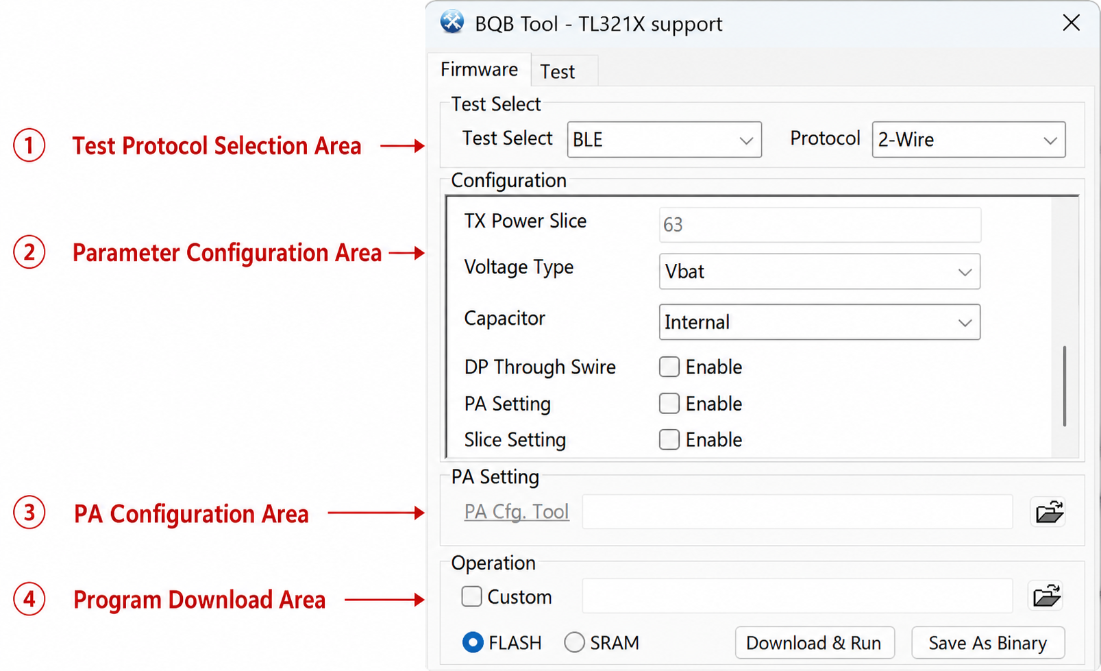
Basic Function Validation
The second function provided by BQB_Tool is basic function validation. It simulates the instruction interaction between the test instrument and the chip:
- Init Command: Configures test parameters (PHY mode, payload length, etc.), and the chip returns the execution status.
- RX Command: Starts the receive test. The chip enters RX mode and counts received packets.
- TX Command: Starts the transmit test. The chip transmits test packets according to the configured parameters.
- END Command: Ends the test. The chip returns the transmitted/received packet count.
With this function, users can quickly verify whether the chip BQB test firmware operates properly without using a test instrument.
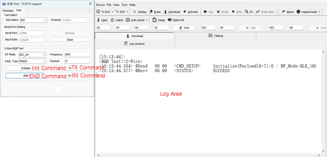
Usage Instructions
Preparation
Hardware Preparation:
| Device | Description |
|---|---|
| EVK Development Board | Development board equipped with the chip under test |
| UART Cable | 2-Wire connection (TX + RX + GND) for connecting the EVK to the test instrument or PC |
| Test Instrument | Such as R&S CMW500/CMW270, used for official BQB qualification testing |
| RF Cable | Connects the EVK antenna port to the RF port of the test instrument |
| DC Power Supply | External power supply if required (optional) |
Software Preparation:
| Software | Description |
|---|---|
| BQB Test Binary | Compile the BQB_Demo project for the corresponding chip in the SDK |
| BDT Tool | Telink Burning and Debugging Tool, which includes BQB_Tool |
| Test Instrument Control Software | Such as CMWrun (R&S), used for automated testing |
General Operation Flow
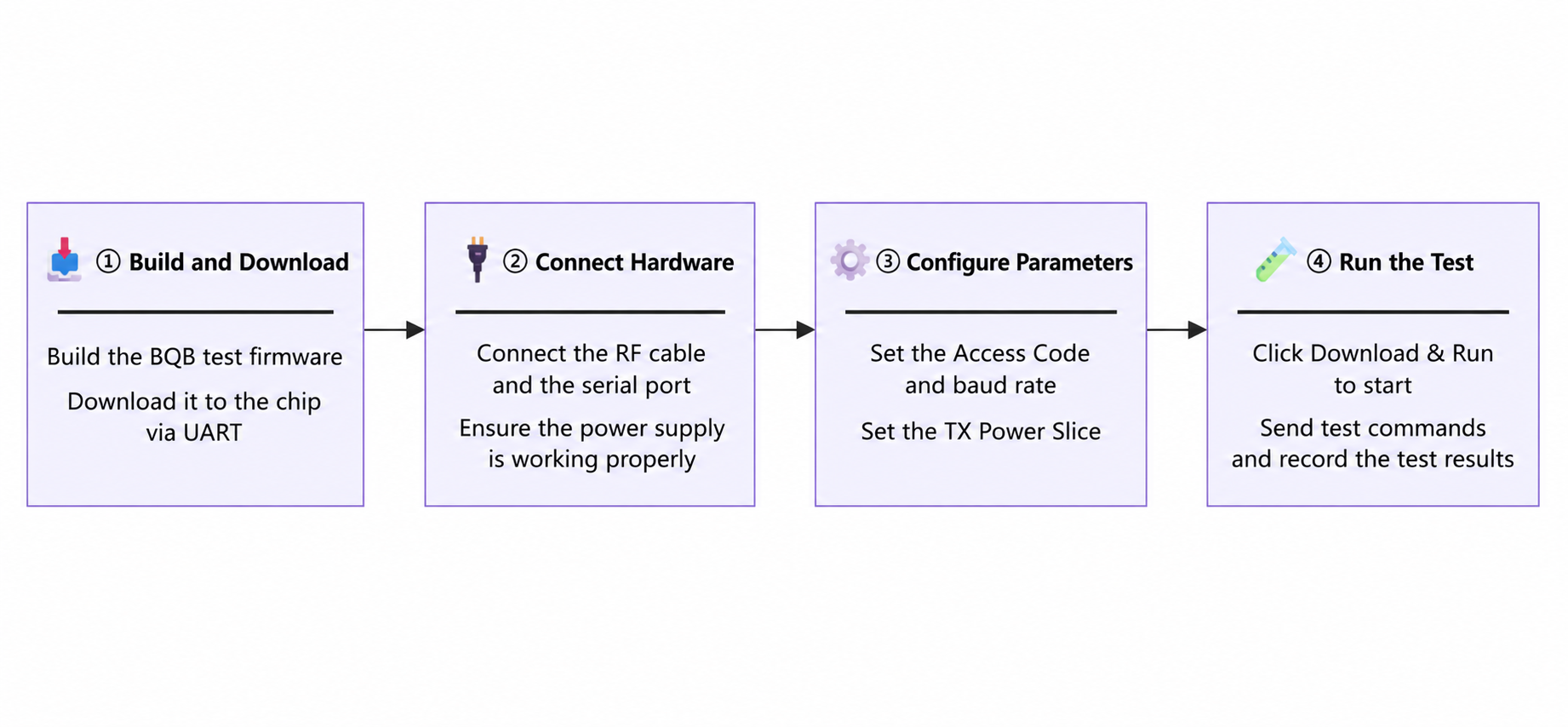
Step 1: Compile and Download the BQB Test Program
- TL Series: Open the
tl_platform_src\demo\vendor\RF_Certification\BQB_Demoproject.- Compile and download the firmware to the chip.
- TC Series: Open the
tc_platform_src\demo\vendor\BQB_EMI_Demoproject.- Ensure that
TEST_DEMOis defined asBQB_DEMOinapp_config.h. - Compile and download the firmware to the chip.
- Ensure that
Step 2: Connect Hardware
Method 1: Connect Directly to the Test Instrument (Official Qualification Testing)
Chip UART TX ────-> Test Instrument UART RX
Chip UART RX ────-> Test Instrument UART TX
Chip GND ────-> Test Instrument GND
Chip RF ────-> Test Instrument RF Port
Method 2: Connect to PC Using BQB_Tool (Function Validation)
Chip UART TX ────-> USB-to-UART RX
Chip UART RX ────-> USB-to-UART TX
Chip GND ────-> USB-to-UART GND
Step 3: Configure Parameters (Optional)
If the default configuration is used, this step can be skipped. To modify the configuration:
- Open BQB_Tool in the BDT tool.
- Modify the required configuration items (UART pins, TX power, PA, etc.).
- Save the configuration and download the firmware again.
Step 4: Perform Testing
Using a Test Instrument: Follow the test instrument operation manual, select the BQB RF test items, and the instrument automatically sends SETUP/RX_TEST/TX_TEST/END commands and collects the test results.
Using BQB_Tool for Validation: Manually send commands in the tool and observe the chip response.
TX Test
Test Items and Specifications:
| Test Item | Bluetooth Specification Requirement | Description |
|---|---|---|
| Output Power | -20 dBm to +20 dBm (BLE) | The default chip transmit power must meet the requirement after calibration |
| Modulation Characteristics | Δf1avg ≥ 225 kHz, Δf2max ≥ 185 kHz (1M) | Frequency deviation characteristics |
| Carrier Frequency Offset | Within ±150 kHz | Frequency accuracy |
| Carrier Frequency Drift | Within ±50 kHz | Frequency stability |
| In-band Spurious Emissions | Adjacent channel ≤ -20 dBm | Spectrum mask compliance |
Test Procedure:
| Step | Operation | Description |
|---|---|---|
| 1 | Compile and Download | Compile the BQB_Demo project for the corresponding chip and download the firmware |
| 2 | Connect the Instrument | Connect the UART interface to the test instrument and connect the RF cable to the RF port of the test instrument |
| 3 | Configure the Instrument | Select the BLE BQB RF TX test item on the test instrument |
| 4 | Automatic Testing | The test instrument automatically sends the SETUP -> TX_TEST -> END command sequence |
| 5 | Check Results | The test instrument displays the TX test results for each item |
Typical Command Sequence:
SETUP: Reset -> BLE 1M mode
TX_TEST: Channel 0 (2402 MHz), Payload = 37 bytes, PRBS9
END: Retrieve transmitted packet count
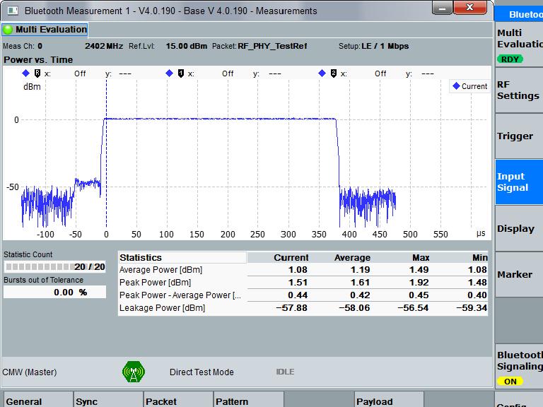
RX Test
Test Items and Requirements:
| Test Item | Bluetooth Specification Requirement | Description |
|---|---|---|
| Sensitivity | ≤ -70 dBm (BLE 1M, PER ≤ 30.8%) | Receiver sensitivity |
| Carrier-to-Interference Ratio (C/I) | Co-channel C/I ≤ 21 dB | Resistance to co-channel interference |
| Blocking Performance | -30 dBm to +27 dBm depending on frequency offset | Resistance to out-of-band interference |
| Maximum Input Level | ≥ -10 dBm (PER ≤ 30.8%) | Maximum received power |
Procedure:
| Step | Operation | Description |
|---|---|---|
| 1 | Compile and download | Compile the BQB_Demo project for the corresponding chip and download the firmware |
| 2 | Connect the instrument | Connect the UART interface to the tester and connect the RF cable to the tester RF port |
| 3 | Configure the Instrument | Select the BLE BQB RF RX test item on the test instrument |
| 4 | Automatic Testing | The test instrument sends the SETUP -> RX_TEST command sequence, sends test packets, and finally sends the END command |
| 5 | Check Results | The test instrument calculates the PER based on the received packet count returned by the chip |
Typical Command Sequence:
SETUP: Reset -> BLE 1M mode
RX_TEST: Channel 0 (2402 MHz), Payload = 37 bytes
(The tester sends 1500 test packets)
END: Obtain received packet count -> Calculate PER
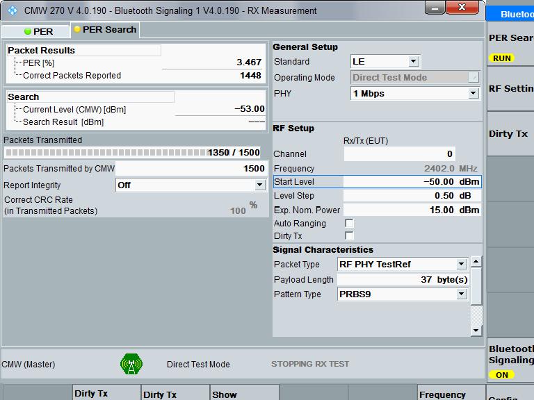
BQB_Tool Usage
When a test instrument is not available, BQB_Tool can be used for simple functional verification:
| Step | Operation | Description |
|---|---|---|
| 1 | Compile and download | Compile the BQB_Demo project for the corresponding chip and download the firmware |
| 2 | Connect the tool | Connect the UART interface to the PC and open BQB_Tool in BDT |
| 3 | Send SETUP | Send the reset command and confirm that the chip returns a successful status |
| 4 | Send TX_TEST | Send the TX test command, and the chip starts transmitting packets |
| 5 | Send END | Send the end command and check the transmitted packet count returned by the chip |
| 6 | Send RX_TEST | Send the RX test command, and the chip enters the receiving state |
| 7 | Send END | Send the end command and check the received packet count returned by the chip (should be 0 because no test instrument is transmitting packets) |
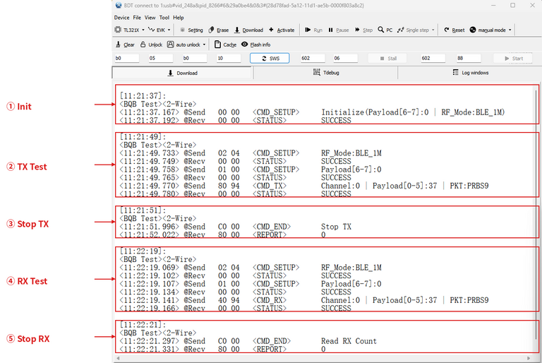
Common Issues and Notes
UART Connection Issues:
- Ensure that the TX/RX pins are connected correctly (TX of one side connects to RX of the other side, and RX connects to TX).
- The default baud rate is 115200. Ensure that the baud rates on both sides are consistent.
- The default UART pins vary depending on the chip model. Refer to the configuration files in the corresponding SDK:
- TL series:
tl_platform_src\demo\vendor\common\common\app_config\bqb_app_config.h(BQB_UART_TX_PORT/BQB_UART_RX_PORTmacros) - TC series:
tc_platform_src\demo\vendor\BQB_EMI_Demo\BQB\bqb.h(BQB_UART_TX_PORT/BQB_UART_RX_PORTmacros)
- TL series:
Access Code Configuration:
- The default Access Code is
0x29417671. - To modify the Access Code, use BQB_Tool or directly modify the
ACCESS_CODEmacro in the source code.
Power Calibration:
- The default transmit power varies between different chips. Before testing, verify the mapping between the power level and the actual output power.
- The power level can be adjusted through BQB_Tool.
PA Configuration:
- When using an external PA (Power Amplifier), configure the PA TX/RX control pins correctly.
- The PA TX and RX pins cannot be the same.
Internal Capacitor Calibration:
- The chip supports both internal capacitor and external capacitor configurations.
- When using the internal capacitor, the calibration value must be read from FLASH/OTP/SRAM.
- The calibration value storage address varies depending on the Flash size. Refer to the calibration header file of the corresponding chip:
- TL series:
tl_platform_src\demo\vendor\common\{chip_model}\calibration\calibration.h(same macro definitions as above) - TC series:
tc_platform_src\demo\vendor\common\{chip_model}\calibration\calibration.h(FLASH_CAP_VALUE_ADDR_64K/FLASH_CAP_VALUE_ADDR_128K/FLASH_CAP_VALUE_ADDR_512K/FLASH_CAP_VALUE_ADDR_1M/FLASH_CAP_VALUE_ADDR_2Mand other macros)
- TL series:
RF EMI
Overview
What is RF EMI testing?
RF EMI (Electromagnetic Interference) testing is a required RF indicator test for wireless chips during certification processes (such as FCC, CE, SRC, etc.). The EMI test firmware enables the chip to transmit specific RF test signals, such as single-tone, modulated, continuous packet, and burst packet signals. Together with measurement equipment such as a spectrum analyzer, it can be used to verify whether RF performance metrics, including transmit power, frequency offset, spurious emissions, and harmonics, comply with regulatory requirements.
Testing tools
The EMI testing program for Telink chips needs to be used together with the host tools:
| Chip Series | Tools | Description |
|---|---|---|
| TL Series | EMI_Tool (BDT) | Provides richer functionality and supports more configurable options. |
| TC Series | Non_Signaling_Test_Tool / EMI_Test_Tool | Standard non-signaling testing tools |
Note
- EMI test programs must be used in conjunction with the corresponding host tool. The tool communicates with the EVK board via the Swire (single-wire) interface, sends parameters to the chip, and after chip parsing, outputs the corresponding RF test signal.
EMI testing tools
Working Principle
The workflow of the EMI testing tool is as follows:
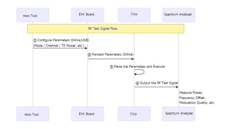
- Users select test modes and configuration parameters in the host tool.
- The host tool writes parameters to the SRAM specified address on the chip via the Swire (or USB-to-Swire) interface.
- The chip firmware polls commands and parameters stored in SRAM and executes the corresponding RF test functions.
- The test signals are output through the antenna port and measured by test equipment such as a spectrum analyzer.
EMI_Test_Tool/Non_Signaling_Test_Tool (TC series chips)
Compatible with TC series chips, supported configuration items include:
- RF mode selection: For specific modes, refer to the datasheet
- Frequency point setting: 2402MHz ~ 2480MHz
- Power settings: multi-level adjustable power
- Test modes: CarrierOnly, Burst (Prbs9/0x55/0x0F), Continue (Prbs9), RX
- Frequency hopping enable: Frequency hopping is supported in Continue mode
- PA Control: Supports TX/RX pin configuration for an external PA.
EMI_Tool (TL series chips)
Applicable to TL series chips, in addition to supporting all EMI_Test_Tool/Non_Signaling_Test_Tool functions, it additionally supports:
- BLE Access Code configuration: Customizable Access Code values for the BLE protocol
- Internal capacitor configuration: Optional to turn off internal capacitors
- PA bypass enable: supports PA bypass mode
- Swire through USB enable: Supports Swire communication via USB.
- Power Slice mode: Supports power slicing testing
- Adaptive interference mitigation: Supports environmental noise detection and pauses packet transmission when the noise level is too high.
- Packet Tone mode: Supports inserting a single-tone signal between packets.
Chip and tool mapping table
| Chip Series | Tools | SDK Path |
|---|---|---|
| TL Series | EMI_Tool | tl_platform_src\demo\vendor\RF_Certification\EMI_Demo |
| TC Series | EMI_Test_Tool/Non_Signaling_Test_Tool | tc_platform_src\demo\vendor\BQB_EMI_Demo |
EMI Modes and Corresponding APIs
Telink chip EMI testing supports the following four basic modes:
| Mode | Command ID (TC series) | Command ID (TL series) | Description |
|---|---|---|---|
| CarrierOnly (Single Tone) | 0x01 | 0x01 | Generates a single-frequency continuous wave signal |
| Continue | 0x02 | 0x02 | Generates a continuous modulation packet signal |
| RX | 0x03 | 0x03 | Receive Mode, Counts received packets and measures RSSI. |
| Burst | 0x04/0x05/0x06 | 0x04 | Generates burst modulation packet signals |
Supported wireless communication modes include: BLE1M, BLE2M, BLE125K, BLE500K, Zigbee250K, Private 2M, and Private 1M.
CarrierOnly (Single Carrier)
Function description:
CarrierOnly mode is used to generate a single-frequency continuous wave signal (unmodulated carrier). In this mode, the frequency, power level, and communication mode can be configured. This mode is mainly used to test indicators such as transmit power, frequency accuracy, and phase noise of the chip.
Spectrum analyzer phenomenon:
The spectrum analyzer displays a single-frequency peak signal with no modulation bandwidth expansion.
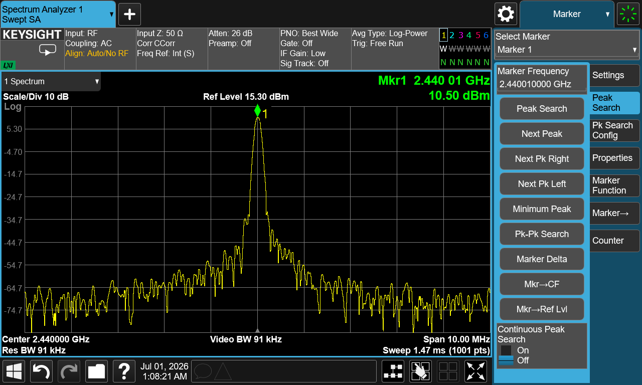
API interfaces:
TL Series:
void emicarrieronly(void);
TC Series:
void emicarrieronly(RF_ModeTypeDef rf_mode, unsigned char pwr, signed char rf_chn);
| Parameters | Description |
|---|---|
| rf_mode | RF mode: refer to each chip demo |
| pwr | Power Level Index |
| rf_chn | Channel Number (Frequency Range: 2402~2480MHz) |
Usage Example:
// TC series
emicarrieronly(RF_MODE_BLE_1M_NO_PN, power_level, 17);  // BLE 1M mode, 2440MHz

// TL series - automatically called after configuration by the host computer
// Host computer settings: Mode = BLE1M, Frequency Point = 2440MHz, Power = 0dBm
// Chip auto-executes emicarrieronly()
Frequency hopping mode:
The TL series CarrierOnly mode supports hopping, allowing switching between multiple frequency points to output a single carrier signal for rapid verification of transmission performance across multiple frequency points.
Continue mode
Function description:
The Continue mode is used to generate continuous modulation signals. In this mode, the chip continuously sends modulated data, allowing settings of frequency point, power value, communication mode, and payload data type.
Supported Payload Data Types:
| pkt_type | Data types | Description |
|---|---|---|
| 0 | PRBS9 (random data) | Pseudo-random sequences simulate real data |
| 1 | 0x0F | Fixed data 0x0F |
| 2 | 0x55 | Fixed Data 0x55 (0101 alternating pattern) |
Spectrum analyzer phenomenon:
The spectrum analyzer displays a modulated signal continuously occupying channel bandwidth, with the signal uninterrupted.
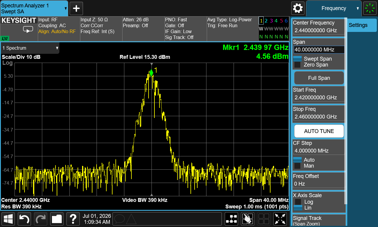
API interfaces:
TL Series:
void emi_tx_continue(void);
TC Series:
void emi_con_prbs9(RF_ModeTypeDef rf_mode, unsigned char pwr, signed char rf_chn);
void emi_con_tx55(RF_ModeTypeDef rf_mode, unsigned char pwr, signed char rf_chn);
void emi_con_tx0f(RF_ModeTypeDef rf_mode, unsigned char pwr, signed char rf_chn);
Frequency hopping mode:
Continue mode supports frequency hopping. After enabling frequency hopping, the chip switches between different frequency points to send continuous packets according to a preset frequency hopping sequence.
Burst mode
Function description:
Burst mode is used to generate burst modulation packet signals. Unlike Continue mode, Burst mode transmits non-continuous packet signals with gaps between packets. Frequency points, power values, communication modes, and payload data types can be set.
Supported Payload data types: Refer to the data types supported by the tool interface
Spectrum analyzer phenomenon:
Because the Burst mode signal is not continuous, the spectrum analyzer needs to use Single Sweep or MaxHold settings to capture the signal:
- Single Sweep: A single scan captures a single burst packet
- MaxHold: Maximum hold. The complete spectrum envelope can be observed after multiple scans are accumulated.
Burst signal under Single Sweep settings:
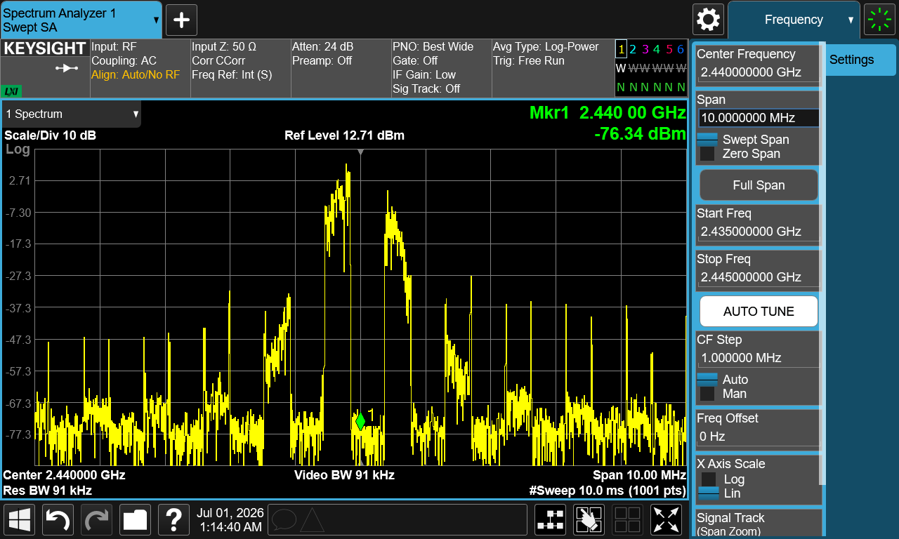
Burst under MaxHold settings:
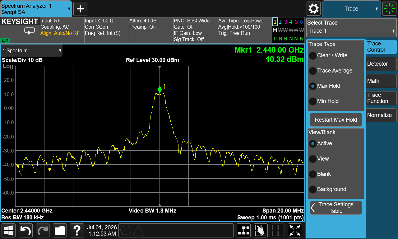
API interfaces:
TL Series:
void emi_tx_burst(void);
TC Series:
void emitxprbs9(RF_ModeTypeDef rf_mode, unsigned char pwr, signed char rf_chn);
void emitx55(RF_ModeTypeDef rf_mode, unsigned char pwr, signed char rf_chn);
void emitx0f(RF_ModeTypeDef rf_mode, unsigned char pwr, signed char rf_chn);
Adaptive Anti-Interference Mode (TL Series):
The TL series Burst mode supports adaptive anti-interference functionality. Once enabled, the chip continuously monitors environmental noise:
- When environmental noise is below -70dBm, Burst packets are sent normally
- When the environmental noise exceeds -70 dBm, packet transmission is paused, and the device switches to RX mode for continuous monitoring.
- Packet transmission automatically resumes when the noise level decreases.
RX mode
Function description:
RX mode is used for receiving tests. In this mode, the chip remains in the receive state and counts the number of received packets and RSSI (Received Signal Strength Indicator) values. Test packets need to be sent together with signal sources (such as comprehensive testers).
Spectrum analyzer phenomenon:
RX mode does not generate RF output signals; instead, the host computer reads the number of packets received and RSSI values through the host computer tools.
API interfaces:
TL Series:
void emirx(void);
TC Series:
void emirx(RF_ModeTypeDef rf_mode, unsigned char pwr, signed char rf_chn);
Data acquisition:
The chip reports the following data to the controller via SRAM:
| SRAM address offset | Content | Description |
|---|---|---|
| +0x04 | RSSI values | Current received signal strength |
| +0x0C | Package counting | The cumulative number of received packets |
Usage Instructions
Preparation
-
Hardware preparation:
- EVK Development Board (equipped with chip under test)
- Swire Cable (connecting EVK to PC)
- Spectrum analyzers (such as Keysight N9020A, etc.)
- RF cable (connecting the EVK antenna port to the spectrum analyzer)
- DC power supply (if external power supply is required)
-
Software preparation:
- EMI test bin file for the corresponding chip (compiling the EMI_Demo project in the SDK)
- Host computer tools: EMI_Tool (TL series) or EMI_Test_Tool/Non_Signaling_Test_Tool (TC series)
General Operation Flow
The general operation process is as follows:
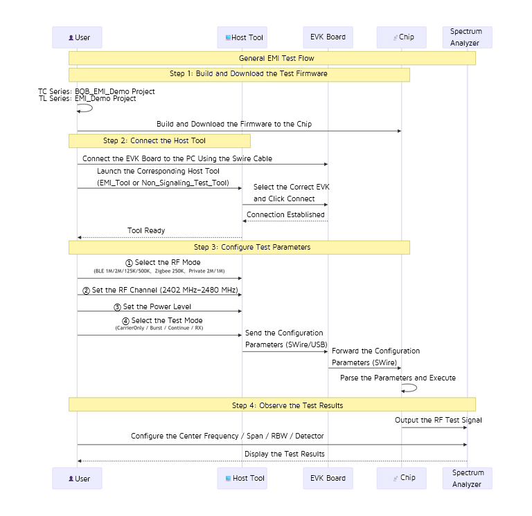
CarrierOnly mode test instructions
| Steps | Operation | Description |
|---|---|---|
| 1 | Choose the tool | TC Series: Non_Signaling_Test_Tool; TL Series: EMI_Tool |
| 2 | Download the test bin | Compiling and downloading the EMI_Demo project for the corresponding chip |
| 3 | Configuration parameters | Mode selection: CarrierOnly; RF mode: BLE1M; Frequency point: 2440MHz; Power: 0dBm |
| 4 | Spectrum instrument settings | Center Freq: 2440MHz, Span: 10MHz, RBW: 100kHz |
| 5 | Observe the phenomenon | The spectrum analyzer displays a single peak signal at 2440MHz |
Continue mode test instructions
| Steps | Operation | Description |
|---|---|---|
| 1 | Choose the tool | TC Series: Non_Signaling_Test_Tool; TL Series: EMI_Tool |
| 2 | Download the test bin | Compiling and downloading the EMI_Demo project for the corresponding chip |
| 3 | Configuration parameters | Mode selection: Continue; RF mode: BLE 1M; Frequency point: 2440MHz; Power: 0dBm; Data type: Prbs9 |
| 4 | Spectrum instrument settings | Center Freq: 2440MHz, Span: 5MHz, RBW: 30kHz |
| 5 | Observe the phenomenon | The spectrum analyzer displays a continuous modulated signal, occupying about 1MHz of bandwidth |
Note
- For frequency hopping testing, enable the Hopping option in the host computer tool.
Burst mode test instructions
| Steps | Operation | Description |
|---|---|---|
| 1 | Choose the tool | TC Series: Non_Signaling_Test_Tool; TL Series: EMI_Tool |
| 2 | Download the test bin | Compiling and downloading the EMI_Demo project for the corresponding chip |
| 3 | Configuration parameters | Mode selection: Burst; RF mode: BLE 1M; Frequency point: 2440MHz; Power: 0dBm; Data type: Prbs9 |
| 4 | Spectrum instrument settings | Center Freq: 2440MHz, Span: 5MHz, RBW: 30kHz, Detector: MaxHold |
| 5 | Observe the phenomenon | After multiple scans using MaxHold, the spectrum analyzer shows discontinuous modulation signal envelopes |
Note
- Since the burst signal is not continuous, it is recommended to use the spectrum analyzer's MaxHold or Single Sweep mode to capture the signal.
RX mode test instructions
| Steps | Operation | Description |
|---|---|---|
| 1 | Choose the tool | TC Series: Non_Signaling_Test_Tool; TL Series: EMI_Tool |
| 2 | Download the test bin | Compiling and downloading the EMI_Demo project for the corresponding chip |
| 3 | Configuration parameters | Mode selection: RX; RF mode: BLE1M; Frequency: 2440MHz |
| 4 | Signal source settings | A comprehensive tester was used to send a BLE 1M test packet, with a frequency point of 2440MHz and a power of 1dBm |
| 5 | Observe the phenomenon | The host computer tool displays the number of packages received and RSSI values |
EMI_Tool Displays the number of packages received and RSSI values (TL Series):
Non_Signaling_Test_Tool Displays the number of packages received and RSSI values (TC Series):
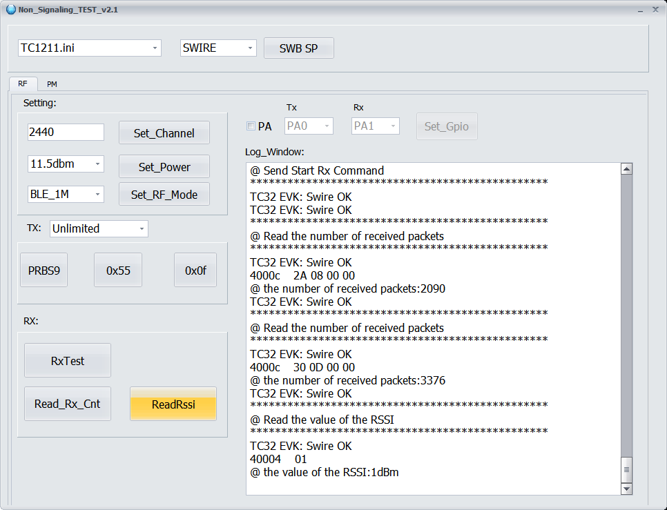
Timer
Introduction
Timer is a general-purpose hardware timer. All chips support the following four modes: TIMER_SYS_CLOCK_MODE, TIMER_GPIO_TRIGGER_MODE, TIMER_GPIO_WIDTH_MODE, and TIMER_TICK_MODE.
Chip Feature Differences Summary
Chips differ in terms of timer channel count, input capture mode, and other aspects, as summarized below:
| Chip | Timer Count | Input Capture Mode |
|---|---|---|
| TC321x / B80/ B80B / B85 / B87 | 3 (TIMER0/1/2) | ❌ |
| B91 / B92 / TL321x / TL751x | 2 (TIMER0/1) | ❌ |
| TL721x / TL322x / TL323x | 2 (TIMER0/1) | ✅ |
Note
- The hardware channels through which GPIO signals connect to the timer also differ across chips, but this is encapsulated by
timer_gpio_init()and requires no attention from general users.
Timer Function
Timer supports four operating modes. All chips support these four basic modes.
System Clock Mode
Clock source: pclk
Function: Generates periodic interrupts. When the counter reaches the capture value, an interrupt is triggered, and the counter automatically reloads the initial_tick and restarts counting, repeating the cycle.
Setup steps (using initial_tick = 0, capture value = 50 ms as an example):
// TC Series
timer0_set_mode(TIMER_MODE_SYSCLK, 0, 50 * sys_clk.pclk * 1000);
timer_start(TIMER0);

// TL Series
timer_set_init_tick(TIMER0, 0);
timer_set_cap_tick(TIMER0, 50 * sys_clk.pclk * 1000);
timer_set_mode(TIMER0, TIMER_MODE_SYSCLK);
timer_start(TIMER0);
Result: LED2 toggles every 50 ms.

GPIO Trigger Mode
Clock source: GPIO edge transitions
Function: A specified number of GPIO rising/falling edges triggers an interrupt. The counter increments by 1 on each rising/falling edge. When the counter reaches the set value, an interrupt is generated, and the counter resets to zero and restarts.
Setup steps:
// TC Series
timer0_gpio_init(SW1, POL_RISING);
timer0_set_mode(TIMER_MODE_GPIO_TRIGGER, 0, TIMER_MODE_GPIO_TRIGGER_TICK);
timer_start(TIMER0);

// TL Series
timer_gpio_init(TIMER0, SW1, POL_RISING);
timer_set_init_tick(TIMER0, 0);
timer_set_cap_tick(TIMER0, TIMER_MODE_GPIO_TRIGGER_TICK);
timer_set_mode(TIMER0, TIMER_MODE_GPIO_TRIGGER);
timer_start(TIMER0);
Note
TIMER_MODE_GPIO_TRIGGER_TICKis a macro defined in the Demo (value0x01), representing the number of GPIO edge transitions required to trigger an interrupt. It is not defined in the driver header file.
Result (using capture value = 0xf, GPIO_PA2 generating a rising edge every 500 ms as an example): LED2 toggles once every 15 rising edges on GPIO_PA2.

GPIO Pulse Width Mode
Clock source: pclk
Function: Captures the GPIO pulse width. When the GPIO detects an edge of the configured polarity, the timer starts, incrementing by 1 for each pclk cycle. When the signal level flips, an interrupt is triggered, and the counter stops. The pulse width is calculated from the captured count value. One-shot mode (no repeat).
Setup steps:
// TC Series
timer0_gpio_init(SW1, POL_FALLING);
timer0_set_mode(TIMER_MODE_GPIO_WIDTH, 0, 0);
timer_start(TIMER0);

// TL Series
timer_gpio_init(TIMER0, SW1, POL_FALLING);
timer_set_mode(TIMER0, TIMER_MODE_GPIO_WIDTH);
timer_start(TIMER0);
Polarity Description: Setting POL_FALLING means the timer starts on a falling edge, and the interrupt is generated on a rising edge.
Result (a rising edge is generated 250 ms after a falling edge on GPIO_PA2, triggering the interrupt): LED2 toggles on the rising edge of GPIO_PA2. The timer register reads 0x005b8e01 = 6000129. At 24 MHz, 6000129 / 24M ≈ 250 ms.

Tick Mode
Clock source: pclk
Function: A time indicator that does not generate interrupts. The counter increments by 1 on each rising edge of pclk. Upon overflow, the counter is automatically reset to zero and starts counting again. Software can manually read or clear the counter value.
Setup steps (using initial_tick = 0, capture value = 0, manually resetting the timer every 500 ms as an example):
// TC Series
timer0_set_mode(TIMER_MODE_TICK, 0, 0);
timer_start(TIMER0);

// TL Series
timer_set_mode(TIMER0, TIMER_MODE_TICK);
timer_start(TIMER0);
Result: LED2 toggles every 500 ms.

Input Capture Mode
The Input Capture Mode is newly introduced, which captures the timer count value upon a GPIO edge transition. Refer to the "Chip Feature Differences Summary" for supported chips.
Capture Modes:
| Mode | Enum Value | Description |
|---|---|---|
| Rising edge capture | TMR_CAPT_RISING_EDGE |
Captures triggered on rising edge |
| Falling edge capture | TMR_CAPT_FALLING_EDGE |
Captures triggered on falling edge |
| Both edges capture | TMR_CAPT_RISING_FALLING_EDGE |
Captures triggered on both rising and falling edges |
Setup steps:
// 1. Configure GPIO and enable capture (select mode 0 or 3 first)
timer_set_init_tick(TIMER0, 0);
timer_set_cap_tick(TIMER0, 0);                    // capt is not used as the mode interrupt trigger value
timer_set_mode(TIMER0, TIMER_MODE_SYSCLK);        // Or TIMER_MODE_TICK
timer_set_input_capture_mode(TIMER0, TMR_CAPT_RISING_FALLING_EDGE, GPIO_PA0);
timer_set_irq_mask(FLD_TMR0_CAPT_IRQ);            // Enable capture interrupt
timer_start(TIMER0);

// 2. Read capture value in interrupt handler
void timer0_irq_handler(void) {
    if (timer_get_irq_status(FLD_TMR0_CAPT_IRQ)) {
        timer_clr_irq_status(FLD_TMR0_CAPT_IRQ);
        unsigned int capt_val = timer_get_capture_value(TIMER0);
        // Calculate PWM period: difference between two consecutive capture values
    }
}
Timer API Differences
TC Series APIs
| Function | Description |
|---|---|
timer0_set_mode(mode, init_tick, cap_tick) |
Sets the Timer0 mode and parameters |
timer1_set_mode(mode, init_tick, cap_tick) |
Sets the Timer1 mode and parameters |
timer2_set_mode(mode, init_tick, cap_tick) |
Sets the Timer2 mode and parameters |
timer0_gpio_init(pin, pol) |
Initializes Timer0 GPIO |
timer1_gpio_init(pin, pol) |
Initializes Timer1 GPIO |
timer_start(type) |
Starts the timer |
timer_stop(type) |
Stops the timer |
timer_set_irq_mask(mask) |
Sets the interrupt mask (reg_irq_mask) |
timer_clr_irq_mask(mask) |
Clears the interrupt mask |
timer_clear_interrupt_status(status) |
Clears the interrupt status |
timer_get_interrupt_status(status) |
Gets the interrupt status |
TL Series APIs
| Function | Description |
|---|---|
timer_set_mode(type, mode) |
Sets the timer mode |
timer_gpio_init(type, pin, pol) |
Initializes GPIO |
timer_set_init_tick(type, init_tick) |
Sets the initial tick |
timer_set_cap_tick(type, cap_tick) |
Sets the capture tick |
timer_start(type) / timer_stop(type) |
Starts the timer |
timer_get_irq_status(status) |
Gets the interrupt status |
timer_clr_irq_status(status) |
Clears the interrupt status |
timer_set_irq_mask(mask) / timer_clr_irq_mask(mask) |
Interrupt mask (reg_tmr_ctrl3) |
timer0_get_tick() / timer1_get_tick() |
Reads the tick value |
timer_set_wrap(type) |
Sets the wrap mode |
In addition to the TL series basic APIs, some chips add input capture and DMA-related interfaces:
| Function | Description |
|---|---|
timer_set_input_capture_mode(type, capt_mode, pin) |
Sets the input capture mode |
timer_input_capture_en(type) |
Enables input capture mode |
timer_input_capture_dis(type) |
Disable input capture (TL721x only) |
timer_get_capture_value(type) |
Reads the capture value (independent of tick) |
timer_reset_tick(type, reset) |
Resets tick value (capture or compare) |
timer_set_rx_dma_config(type, chn) |
Configures DMA receive channel |
timer_receive_dma(type, addr, rev_size) |
Starts DMA receive |
timer_set_dma_chain_llp(type, chn, dst, len, head) |
Configures DMA chain head node |
timer_set_rx_dma_add_list_element(...) |
Adds DMA chain element |
GPIO Interrupt Routing Differences
The Timer GPIO Trigger Mode, GPIO Pulse Width Mode, and Input Capture Mode require routing external GPIO signals to the Timer module as the counting clock source. The routing mechanisms supported by different chips are described in the "Chip Feature Differences Summary".
Routing Principle
GPIO signals must pass through hardware routing channels before reaching the Timer module. Each Timer instance is fixedly mapped to one routing channel. The GPIO pin level signal is routed to the Timer counter through the selected routing channel after polarity selection (rising edge/falling edge).
Principle: The signal can be used either as a GPIO interrupt source to trigger CPU interrupts or as the Timer counting clock. The Timer GPIO modes only use the counting function and do not require enabling the GPIO interrupt mask. Otherwise, additional GPIO interrupts will be generated, causing frequent interrupt entry and exit.
The Timer and routing channel mapping relationships for different chips are as follows:
| Timer Channel | RISC Register Routing | gpio2risc Routing | PLIC GPIO_IRQ Routing (TL321x/TL322x/TL323x) | PLIC GPIO_IRQ Routing (TL751x) |
|---|---|---|---|---|
| TIMER0 | gpio_risc0 | gpio2risc0 | GPIO_IRQ1 | GPIO_IRQ0 |
| TIMER1 | gpio_risc1 | gpio2risc1 | GPIO_IRQ2 | GPIO_IRQ1 |
| TIMER2 | gpio_risc2 | - | - | - |
RISC Register Routing
Use the reg_gpio_irq_risc0_en(pin) / reg_gpio_irq_risc1_en(pin) / reg_gpio_irq_risc2_en(pin) registers to bind the specified GPIO to the corresponding RISC channel. Use reg_gpio_pol(pin) to set the trigger polarity, and use reg_irq_src (FLD_IRQ_GPIO_RISC0_EN / FLD_IRQ_GPIO_RISC1_EN) to enable the interrupt source.
The driver interfaces timer0_gpio_init(pin, pol) / timer1_gpio_init(pin, pol) already encapsulate the above configuration. Do not call gpio_set_risc_irq_mask() again to enable the RISC mask (otherwise a GPIO interrupt will be generated).
gpio2risc Routing
Use gpio_set_gpio2risc0_irq(pin, pol) / gpio_set_gpio2risc1_irq(pin, pol) to bind the GPIO to the gpio2risc channel, and use gpio_gpio2risc0_irq_en(pin) / gpio_gpio2risc1_irq_en(pin) to enable the channel.
The driver interface timer_gpio_init(type, pin, pol) already encapsulates the above configuration.
PLIC GPIO_IRQ Routing
The routing is implemented through independent interrupt channels in the PLIC: gpio_set_irq(GPIO_IRQn, pin, trigger_type) maps the GPIO to the corresponding channel, and gpio_set_irq_mask(GPIO_IRQ_IRQn) enables the interrupt channel mask. Note that the channel numbers for TL751x differ from other chips.
The driver interface timer_gpio_init(type, pin, pol) already encapsulates the above configuration.
Commonality: The timer_gpio_init interface on all chips internally performs GPIO input enable, pull-up/pull-down resistor configuration (pull-up for falling-edge triggering and pull-down for rising-edge triggering), polarity configuration, and routing configuration. Users do not need to manually configure GPIO registers.
Notes
Mode Setting Sequence
When configuring the Timer mode, configure init_tick and cap_tick first, then call timer_set_mode(), and finally call timer_start(). The timer_set_mode() function clears the existing interrupt status internally. Calling it first will overwrite the tick values configured later.
// Correct sequence (TL series)
timer_set_init_tick(TIMER0, 0);
timer_set_cap_tick(TIMER0, 50 * sys_clk.pclk * 1000);
timer_set_mode(TIMER0, TIMER_MODE_SYSCLK);
timer_start(TIMER0);
Interrupt Status Clearing Sequence
After entering the interrupt handler, the interrupt flag must be cleared first before performing any application processing; otherwise, the interrupt may be triggered repeatedly.
// TL series
void timer_irq_handler(void) {
    if (timer_get_irq_status(FLD_TMR0_MODE_IRQ)) {    // status bit
        timer_clr_irq_status(FLD_TMR0_MODE_IRQ);     // 1. Clear the flag first
        // 2. Business logic handling
    }
}

// TC series
void timer_irq_handler(void) {
    if (timer_get_interrupt_status(TMR_STA_TMR0)) {
        timer_clear_interrupt_status(TMR_STA_TMR0);  // 1. Clear the flag first
        // 2. Business logic handling
    }
}
Note
FLD_TMR0_MODE_IRQis an interrupt status bit (timer_irq_eenum) used to query and clear interrupt status.FLD_TMR0_MODE_MASKis an interrupt mask bit (timer_mask_eenum) used bytimer_set_irq_mask()/timer_clr_irq_mask()to enable or disable interrupts. The two bits must not be mixed.
GPIO Pulse Width Mode Single Trigger
GPIO Pulse Width Mode automatically stops counting after triggering an interrupt once and does not run cyclically. For continuous measurement, timer_start(TIMER0) must be called again in the interrupt handler to restart the timer.
Tick Mode Without Interrupt
Tick Mode does not generate interrupts and can only determine the elapsed time by polling timer0_get_tick(). Interrupt mask configuration is not required in this mode and has no effect if configured.
GPIO Routing Resource Occupancy
GPIO Trigger Mode, GPIO Pulse Width Mode, and Input Capture Mode occupy the GPIO routing channel of the corresponding Timer (see the routing table in Chapter 4):
- The three GPIO modes of the same Timer are mutually exclusive and cannot be used simultaneously.
- The occupied routing channel cannot be used for regular GPIO external interrupts.
- TIMER0 and TIMER1 occupy their own routing channels and are independent of each other.
Input Capture Mode Dependency on Basic Modes
The Input Capture function (supported chips are listed in the "Chip Feature Differences Summary") requires System Clock Mode or Tick Mode to be configured first as the counting time base, followed by the capture mode configuration. In this mode, cap_tick is no longer used as an interrupt trigger value, but only as the tick reset point (together with timer_reset_tick()).
DMA Receive Configuration Sequence
When using DMA to transfer captured values, DMA must be configured first before enabling Input Capture Mode. Otherwise, a capture event may occur before DMA is ready, resulting in data loss:
// 1. Configure DMA first
timer_set_rx_dma_config(TIMER0, DMA_CH0);
timer_receive_dma(TIMER0, (unsigned char *)capt_buff, sizeof(capt_buff));
// 2. Then enable capture
timer_set_input_capture_mode(TIMER0, TMR_CAPT_RISING_EDGE, GPIO_PA0);
API Styles Must Not Be Mixed
The TC-style APIs (such as timer0_set_mode(mode, init, cap)) and TL-style APIs (such as timer_set_mode(type, mode) + timer_set_init_tick() + timer_set_cap_tick()) must not be mixed. When porting code, replace the entire API set instead of mixing APIs from different styles.
System Timer (STimer)
Introduction
System Timer (STimer) is a system time benchmark that provides basic time services and interrupt functions.
STimer Function Description
Example of using the Basic Time Service APIs
STimer provides system time, delay, and timeout detection functions. API names vary slightly across chip series, but usage is the same. For detailed interfaces, refer to the STimer API Differences.
Usage example:
// 1. Get the current system time as a reference point
unsigned int ref = stimer_get_tick();  TL Series; TC series uses clock_time()

// 2. Execute a piece of code or a delay
delay_ms(100);  TL Series; TC Series sleep_ms (100)

// 3. Check if there is a timeout (unit: us)
if (clock_time_exceed(ref, 1000)) {
    // More than 1 ms has elapsed
}
Overview with clock sources
STimer is a 32-bit system timer, with clock sources all sourced from onboard 24M crystals: some chips use 24M directly, while others use a 24M xtal to obtain 16M after a 2/3 divider and are supplied to STimer.
| Chip Series | Frequency |
|---|---|
| B80/B80B/B85/B87/TC321x/TC123x/B91 | 16 MHz |
| TC122x/B92/TL321x/TL721x/TL322x/TL323x/TL751x | 24 MHz |
STimer interrupt trigger conditions
The STimer interrupt trigger condition is the most important difference among chip series. During porting, the trigger condition must be confirmed first: whether it uses 32-bit full matching (tick_now == tick_capture) or range matching (within 1/64 of a cycle). With full matching, the interrupt cannot be triggered after the scheduled time has passed; with range matching, the interrupt can still be triggered after the scheduled time has passed.
Note
- 32-bit full matching: triggered only when the current tick and capture value are exactly equal; If the set time has already passed the capture value, it will not be triggered again. Since STimer's current tick is always 0 for the lower 3 bits, the capture tick interface will automatically mask the lower 3 bits to 0.
- Range Matching: The interrupt can be triggered as long as the current tick falls within the
[capture, capture + 2^26)range. This means the interrupt can still be triggered after the configured time has passed (within 1/64 of a cycle). This mechanism applies to scenarios in the application SDK where the theoretical STimer tick value is calculated based on remote time.
| Trigger types | Trigger conditions | Whether the interrupt can still be triggered after the scheduled time has passed | Chip Series |
|---|---|---|---|
| 32-bit full matching | tick_now & BIT[31:3] == tick_capture |
No | B80/B80B/B87/TC321x/TC122x |
| Scope matching | (tick_now - tick_capture) & BIT[31:26] == 0 |
Yes | B85/TC123x/B91/B92/TL321x/TL721x/TL322x/TL323x/TL751x |
Example of Delay Triggering (Range Matching Chip):
For chips using range matching, the interrupt is triggered immediately even if the capture value is set to a time in the past (as long as it is still within 1/64 of a cycle). The following example verifies this feature:
stimer_set_irq_capture(stimer_get_tick() - 10 * SYSTEM_TIMER_TICK_1MS);
// Due to range matching, the interrupt is triggered immediately even if it is 10 ms late (still within 1/64 of a cycle)
Note
- Fully matched chips (B80/B80B/B87/TC321x/TC122x) do not have this feature and cannot trigger interrupts when the scheduled time has passed.
Interrupt function and APIs
STimer generates interrupts at specified moments by setting capture values.
Configuration example (based on TL series STimer_Demo):
// 1. Set the capture value to trigger the interrupt after 1s
stimer_set_irq_capture(stimer_get_tick() + SYSTEM_TIMER_TICK_1S);

// 2. Enable the STimer interrupt (mask macro names may vary slightly depending on the chip)
stimer_set_irq_mask(FLD_SYSTEM_IRQ_MASK);

// 3. Enable the PLIC interrupt and global interrupt
plic_interrupt_enable(IRQ_SYSTIMER);
core_interrupt_enable();

// 4. Interrupt service function (registered to IRQ_SYSTIMER)
_attribute_ram_code_sec_ void stimer_irq_handler(void)
{
    if (stimer_get_irq_status(FLD_SYSTEM_IRQ)) {
        gpio_toggle(LED2);
        stimer_clr_irq_status(FLD_SYSTEM_IRQ);                       // Clear the interruption flag
        stimer_set_irq_capture(stimer_get_tick() + SYSTEM_TIMER_TICK_1S);  // Reset the next trigger
    }
}
PLIC_ISR_REGISTER(stimer_irq_handler, IRQ_SYSTIMER);
TC Series Equivalent Configuration:
stimer_set_capture_tick(clock_time() + 100 * CLOCK_SYS_CLOCK_1MS);
stimer_set_irq_mask(FLD_SYSTEM_IRQ_MASK);
irq_set_mask(FLD_IRQ_SYSTEM_TIMER_EDG_EN);  // TC321x uses FLD_IRQ_SYSTEM_TIMER
irq_enable();

// Interrupt handling
void irq_handler(void)
{
    if (stimer_get_irq_status()) {
        stimer_clr_irq_status();
        stimer_set_capture_tick(clock_time() + 100 * CLOCK_SYS_CLOCK_1MS);
    }
}
STimer API differences
| Function | TC series APIs | TL series APIs |
|---|---|---|
| Get system time | clock_time |
stimer_get_tick |
| Set the tick value | stimer_set_tick |
stimer_set_tick |
| Delay | sleep_us / sleep_ms |
delay_us / delay_ms |
| Timeout check | clock_time_exceed |
clock_time_exceed |
| Set interrupt capture | stimer_set_capture_tick |
stimer_set_irq_capture |
| Interrupt masks | stimer_set_irq_mask / stimer_clr_irq_mask |
stimer_set_irq_mask / stimer_clr_irq_mask |
| Interrupt status | stimer_get_irq_status / stimer_clr_irq_status |
stimer_get_irq_status / stimer_clr_irq_status |
PWM
PWM Overview
The PWM (Pulse Width Modulation) module is used to generate square-wave signals with configurable duty cycles and periods, and can be widely applied in scenarios such as LED dimming, motor control, infrared transmission, and audio DAC driving.
The differences between chips equipped with PWM modules are shown in the table below:
| Chip | Channel Number | 32K Clock Source | Align Mode | Phase-Shifting Function | Pin Configuration API |
|---|---|---|---|---|---|
| B80 / B80B / B85 / B87 / TC321x / TC122x / TC123x | 6 channels(PWM0~PWM5) | Not support | Edge align | Not support | No dedicated interface (fixed pin mapping) |
| B91 | 6 channels(PWM0~PWM5) | Support | Edge align | Not support | pwm_set_pin |
| B92 / TL751x / TL321x / TL323x | 6 channels(PWM0~PWM5) | Support | Edge align + Center align | Support | pwm_set_pin |
| TL721x | 7 channels(PWM0~PWM6) | Support | Edge align + Center align | Support | pwm_set_pin |
| TL322x | 24 channels(PWM0~PWM23) | Support | Edge align + Center align | Support | pwm_set_pin |
Note
- B91 includes TLSR951x and TLSR921x, B92 includes TLSR952x and TLSR922x, B80 includes TLSR8208A/B/C/D and TLSR8373E/F, B80B includes TLSR8208E/F/G/H/J and TLSR8373A/B/C/FBR, B85 includes TLSR825x and TLSR8359, B87 includes TLSR827x and TLSR8355.
General Features: All chips support the pclk clock source, 5 operating modes (PWM0) + continuous (other channels), IR FIFO mode, IR DMA FIFO mode, DMA chained transfer, Invert/Polarity, and N-channel invert.
Modes supported by PWM0:
- Continuous mode
- Counting mode
- IR mode
- IR FIFO mode
- IR DMA FIFO mode
Channels other than PWM0 support only continuous mode.
Clock
The PWM has two clock sources: pclk or 32kHz.
PCLK Clock Source
Function: Supports frequency division. The divided clock is used as the PWM clock source.
Note
Ensure that pclk_frequency is an integer multiple of pwm_frequency; otherwise, the PWM output is not at the expected frequency.
Interface Configuration:
static inline void pwm_set_clk(unsigned int pwm_clk_div);
Where: pwm_clk_div = (pclk_frequency / pwm_frequency) - 1
32kHz Clock Source
Function: Does not support frequency division and only supports continuous mode and counting mode. This configuration is primarily intended to allow PWM waveform output even in suspend mode.
Interface Configuration:
// Chips other than the TL322x
static inline void pwm_32k_chn_en(pwm_clk_32k_en_chn_e pwm_32K_en_chn);
static inline void pwm_32k_chn_dis(pwm_clk_32k_en_chn_e pwm_32K_en_chn);

// TL322x
static inline void pwm_32k_chn_en(pwm_id_e id);
static inline void pwm_32k_chn_dis(pwm_id_e id);
Note
- All channels default to the pclk clock source. To use the 32kHz clock source, call
pwm_32k_chn_ento enable the corresponding channel. Channels that are not enabled continue to use the pclk clock source. - The 32kHz clock source was designed only for suspend scenarios. When using interrupts in continuous mode or counting mode, the interrupt is entered one 32kHz clock cycle early. During this 32kHz clock cycle, the interrupt is exited and re-entered. If an interrupt is needed when using 32kHz PWM, it is recommended to use a GPIO interrupt instead.
- When the PWM clock source is 48 MHz and the duty cycle is strictly 50% (ideal square wave), the theoretical maximum frequency of the PWM output waveform is 24 MHz. Each output cycle requires at least 2 PWM clock cycles (1 cycle high, 1 cycle low). Maximum PWM output frequency = pwm_frequency / 2.
Duty Cycle
A PWM signal frame consists of two parts: Count status (high-level duration) and Remaining status (low-level duration). The specific waveform of a signal frame is shown below, where tmax is the cycle time.
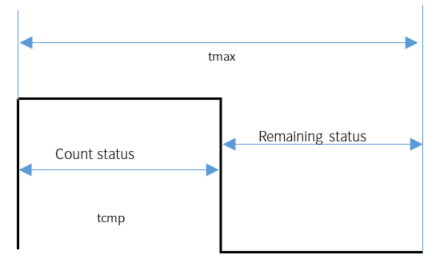
In the driver, the functions for setting the signal frame cycle and duty cycle both use tcmp and tmax as parameters, correspond to registers TCMP/TMAX.
General Duty Cycle Configuration Interface
static inline void pwm_set_tcmp(pwm_id_e id, unsigned short tcmp);
static inline void pwm_set_tmax(pwm_id_e id, unsigned short tmax);
Parameter description:
id: Selects which PWM channel.tcmp: Sets the high-level duration.tmax: Sets the cycle period.
Note
- The parameter sets the PWM cycle, its parameter type is short. The minimum value of tmax is 1 and cannot be 0. If it is 0, the PWM is in a non-operating state. Therefore, the valid range of tmax is: 1~65535.
- The parameter sets the PWM duty cycle, its parameter type is short. The minimum value of tcmp can be 0, in which case the PWM waveform is always low. The maximum value can be tmax, in which case the PWM waveform is always high. Therefore, the valid range of tcmp is: 0~tmax.
- When
pwm_set_tcmp()orpwm_set_tmax()is called while the PWM is actively transmitting, the new value takes effect at the beginning of the next cycle.
IR FIFO Mode and IR DMA FIFO Mode Shadow Interface
When using PWM0 in IR FIFO Mode or IR DMA FIFO Mode, an additional function interface is used:
static inline void pwm_set_pwm0_tcmp_and_tmax_shadow(unsigned short max_tick, unsigned short cmp_tick);
Note
The parameter max_tick sets the cycle of PWM0, and the parameter cmp_tick sets the high-level duration of PWM0. The range of max_tick is: 1~65536, and the range of cmp_tick is: 0~max_tick.
Pulse Count Configuration Interface
When using PWM0 in counting mode or IR mode, the number of output pulses needs to be set. The function interface used is:
static inline void pwm_set_pwm0_pulse_num(unsigned short pulse_num);
pulse_num: The number of pulses. The maximum value that can be written to the register is 14 bits. Range: 0~16383.
IR FIFO Configuration Data Interface
When writing cfg data to the FIFO for PWM0, the function interfaces used are:
static inline void pwm_set_pwm0_ir_fifo_cfg_data(unsigned short pulse_num, unsigned char use_shadow, unsigned char carrier_en);
static inline unsigned short pwm_cal_pwm0_ir_fifo_cfg_data(unsigned short pulse_num, unsigned char shadow_en, unsigned char carrier_en);
use_shadow:
- 1: Use the cycle and duty cycle set by the
pwm_set_pwm0_tcmp_and_tmax_shadowfunction. - 0: Use the cycle and duty cycle set by the
pwm_set_tmaxandpwm_set_tcmpfunctions.
carrier_en:
- 1: Output pulses according to the settings of the pulse_num and use_shadow parameters.
- 0: Output low level, with the duration calculated based on the pulse_num and use_shadow parameters.
Alignment Mode
For chips that support center alignment, see the "Summary Table of Chip Feature Differences" in PWM Overview. PWM supports two alignment modes: edge alignment (default) and center alignment. Chips that support only edge alignment cannot enable center alignment.
Edge-Aligned
In this mode, the waveform of each cycle is aligned at the edge. (PWM2 waveform)
Center-Aligned
In this mode, the waveforms of two consecutive cycles are aligned at the center point (PWM1 waveform).

Interface Configuration:
static inline void pwm_set_align_en(pwm_id_e id);   // Enable center alignment
static inline void pwm_set_align_dis(pwm_id_e id);  // Disable center alignment (restore edge alignment)
Phase Shift Function
For chips that support the phase-shift function, see the "Summary Table of Chip Feature Differences" in PWM Overview. The PWM phase shift function allows setting the phase offset time of the PWM. The phase offset time only takes effect before the first cycle (in the figure below, PWM2 has a phase offset time of 25 \(\mu\)s).

Interface Configuration:
static inline void pwm_set_shift_time(pwm_id_e id, unsigned short shift_clk_num);
Note
- The phase shift time must be set before setting the duty cycle and cycle period.
- If you want to reconfigure the phase shift time, you must reconfigure tcmp and tmax after reconfiguring the phase shift time (regardless of whether the tcmp and tmax values need to be modified).
- If you only want to reconfigure tcmp and tmax, you only need to configure tcmp and tmax without first configuring the phase shift time.
Invert/Polarity
For the waveform set by the duty cycle interface, by default, the high level (Count status) is output first, followed by the low level (Remaining status).
Difference between Invert and Polarity:
- Invert function: Enabling the invert function of a PWM channel via
pwm_invert_eninverts the PWM_PIN waveform. It takes effect regardless of whether the PWM is started. Therefore, if the invert function is enabled before the PWM starts, the initial low level is also inverted to a high level (the initial level defaults to low and cannot be modified). After the PWM starts, the output follows this rule: Count status outputs low, Remaining status outputs high.

- Polarity function: Enabling the polarity function of a PWM channel via
pwm_set_polarity_enonly takes effect after the PWM is started, so it does not invert the initial level before the PWM starts. After the PWM starts, the output follows this rule: Count status outputs low, Remaining status outputs high.

Note
- The Invert and Polarity functions cannot be enabled simultaneously; only one of them can be selected.
- After the PWM starts, the Invert and Polarity functions take effect immediately without waiting for the next cycle.
Related Interfaces:
static inline void pwm_invert_en(pwm_id_e id);      // Enable PWM output inversion
static inline void pwm_invert_dis(pwm_id_e id);     // Disable PWM output inversion
static inline void pwm_n_invert_en(pwm_id_e id);    // Enable PWM_N output inversion
static inline void pwm_n_invert_dis(pwm_id_e id);   // Disable PWM_N output inversion
static inline void pwm_set_polarity_en(pwm_id_e id);  // Enable polarity inversion
static inline void pwm_set_polarity_dis(pwm_id_e id); // Disable polarity inversion
Functional Description
Continuous mode
In this mode, signals are continuously sent according to the configured duty cycle. To stop, call stop, and it stops immediately. During transmission, the duty cycle can be updated, and the new duty cycle takes effect in the next frame.
(1) Experimental Results

The figure above shows the experimental results captured with a logic analyzer:
- Channel 0 (LED1): PWM output signal.
- Channel 1 (LED4): Interrupt indicator GPIO. An interrupt is generated each time a signal frame is sent.
Red box explanation: The delay in interrupt generation is due to the software and hardware processing time required for the CPU to enter the interrupt.
(2) Stop Verification
The following experiment verifies that in continuous mode, after executing stop, the signal stops immediately.
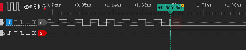
As shown in the figure, after LED3 toggles, the PWM signal stops immediately.
(3) Duty Cycle Update Verification
The following experiment verifies that in continuous mode, the duty cycle can be updated during transmission, and the updated duty cycle takes effect in the next frame.
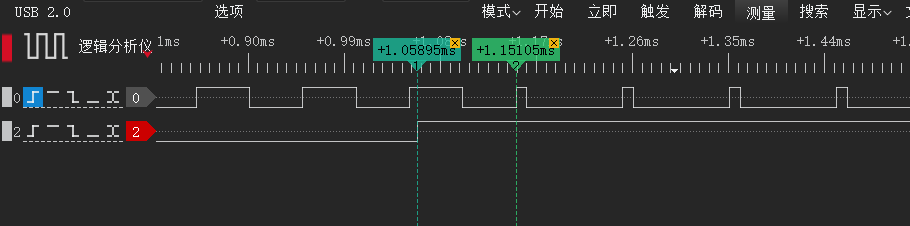
As shown in the figure, after LED3 toggles, the PWM duty cycle is modified and takes effect in the next frame.
Configuration Interface:
pwm_set_pwm0_mode(PWM_NORMAL_MODE);  // Set PWM0 mode
pwm_start(FLD_PWM0_EN);              // Start PWM
pwm_stop(FLD_PWM0_EN);               // Stop PWM
Counting Mode
Sends the configured number of signal frames and then stops. In this mode, calling stop stops it immediately. During transmission in this mode, modifying the duty cycle does not change it.
(1) COUNT_FRAME_INIT Experimental Results

- Channel 0 (LED1): PWM output signal.
- Channel 1 (LED4): Interrupt indicator GPIO. An interrupt is generated each time a signal frame is sent.
Red box explanation: The delay in interrupt generation is due to the software and hardware processing time required for the CPU to enter the interrupt.
(2) COUNT_PNUM_INIT Experimental Results

Details of the red box are as follows:
- Channel 0 (LED1): PWM output signal.
- Channel 1 (LED4): Interrupt indicator GPIO. An interrupt is generated after the specified number of pulses have been sent.
Red box explanation: The 3 \(\mu\)s excess over 50 \(\mu\)s indicates a certain delay in entering the interrupt, due to the software and hardware processing time required for the CPU to enter the interrupt.
(3) Stop Verification
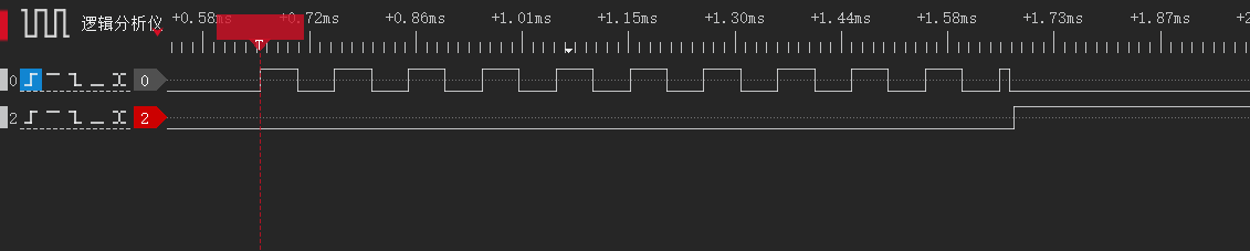
As shown in the figure, after LED3 toggles, the PWM signal stops immediately.
(4) Duty Cycle Verification
The following experiment verifies that in counting mode, the duty cycle cannot be changed during transmission.

As shown in the figure, after LED3 toggles, the PWM signal does not change.
Configuration Interface:
pwm_set_pwm0_mode(PWM_COUNT_MODE);
pwm_set_pwm0_pulse_num(PWM_PULSE_NUM);  // Set the number of pulses
pwm_start(FLD_PWM0_EN);
IR Mode
IR mode continuously sends pulse groups. The duty cycle can be changed in between, and it takes effect in the next pulse group. To stop immediately, you can call stop directly. The difference between IR mode and counting mode is that counting mode stops after sending one pulse group, while IR mode continuously sends pulse groups.
(1) Experimental Results

- Channel 0 (LED1): PWM output signal.
- Channel 1 (LED3): Interrupt indicator GPIO. Toggles once for each pulse group is sent.
Red box explanation: The delay in interrupt generation is due to the software and hardware processing time required for the CPU to enter the interrupt.
(2) Stop Verification
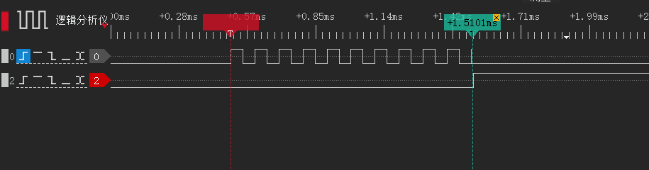
As shown in the figure, after LED3 toggles, the PWM signal stops immediately.
(3) Duty Cycle Update Verification
The following experiment verifies that in IR mode, the duty cycle can be changed in between, but it takes effect after the current pulse group finishes executing.
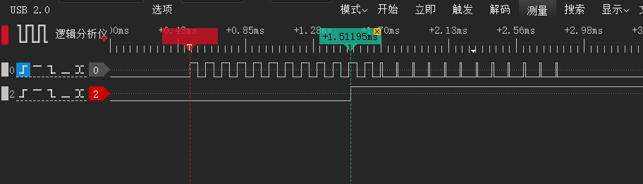
As shown in the figure, after LED3 toggles, the PWM signal does not change immediately, it takes effect only after the current pulse group completes executing.
To stop IR mode while completing the current pulse group, you can switch to counting mode.
To stop immediately, you can call stop directly.
Note
- To stop IR mode while completing the current pulse group, you can switch to counting mode in the interrupt. However, during the switch, the current pulse group in IR mode finishes sending before the switch takes effect.
Configuration Interface:
pwm_set_pwm0_mode(PWM_IR_MODE);
pwm_set_pwm0_pulse_num(PWM_PULSE_NUM);  //set the pulse number in each pulse group
pwm_start(FLD_PWM0_EN);
IR FIFO mode
Without MCU intervention, long code patterns can be sent. The IR carrier frequency is obtained by dividing the system clock and can support common frequencies. The "Fifo cfg data" element serves as the basic unit of the IR waveform. The hardware parses the cfg information and emits the corresponding signal.
(1) Experimental Results
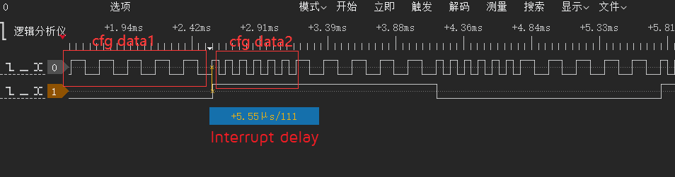
- Channel 0 (LED1): PWM output signal.
- Channel 1 (LED4): Interrupt indicator GPIO. Toggles once when the number of cfg data entries in the FIFO is less than (not including equal to) the configured value (trigger_level is 1).
Red box explanation: The delay in interrupt generation is due to the software and hardware processing time required for the CPU to enter the interrupt.
(2) Stop Verification
The following experiment verifies that in IR FIFO mode, after executing stop, only the execution of the current cfg data is stopped, without affecting the execution of subsequent cfg data in the FIFO.
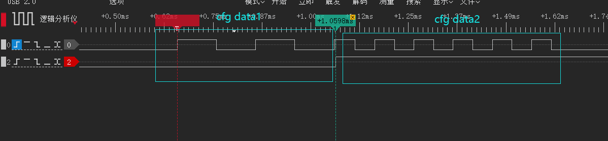
As shown in the figure, after executing stop, LED3 toggles, stopping the execution of the current cfg data 1 without affecting the execution of the subsequent cfg data 2 in the FIFO.
IR FIFO Mode sequentially retrieves cfg data from the FIFO and emits the corresponding signal until the FIFO is empty. In this mode, stop can be used, but it only stops the execution of the current cfg data without affecting the execution of subsequent cfg data in the FIFO.
Note
- In IR FIFO mode, as long as there is data in the FIFO, it is continuously sent out (automatically) without needing a start signal. Similarly, IR DMA FIFO Mode does not need a start signal. However, in other modes, the
pwm_startsignal is required. - Each time the function
pwm_set_pwm0_ir_fifo_cfg_datais called, the FIFO count increments by 1 (if the FIFO is full at this time, it waits until the FIFO is not full before writing). Each time the hardware retrieves one entry from the FIFO, the FIFO count decrements by 1. The FIFO depth is 8 bytes. After data is retrieved from the FIFO, the signal transmission action is executed. The next entry is retrieved from the FIFO only after the current signal has finished executing.
FIFO Status Query Interfaces:
static inline unsigned char pwm_get_pwm0_ir_fifo_data_num(void);   // Get the number of data entries in the FIFO
static inline unsigned char pwm_get_pwm0_ir_fifo_is_empty(void);   // Check if the FIFO is empty
static inline unsigned char pwm_get_pwm0_ir_fifo_is_full(void);    // Check if the FIFO is full
static inline void pwm_clr_pwm0_ir_fifo(void);                     // Clear FIFO data
Configuration Interface:
pwm_set_pwm0_mode(PWM_IR_FIFO_MODE);
pwm_set_pwm0_ir_fifo_cfg_data(PWM_PULSE_NUM1, 1, 1);  // Write FIFO configuration data
pwm_set_pwm0_ir_fifo_cfg_data(PWM_PULSE_NUM2, 0, 1);
IR DMA FIFO Mode
IR DMA FIFO mode is similar to IR FIFO mode, except that the configuration is not directly written to the FIFO by the MCU but is written to the FIFO via DMA.
(1) PWM_IR_FIFO_DMA Experimental Results

- Channel 0 (LED1): PWM output signal.
- Channel 1 (LED4): Interrupt indicator GPIO.
As shown in the figure above, in this mode, the interrupt is triggered only after all cfg data entries in the FIFO have been executed, which differs from the interrupt mechanism in IR FIFO Mode.
The figure below is an enlarged view of the red box in the above figure:
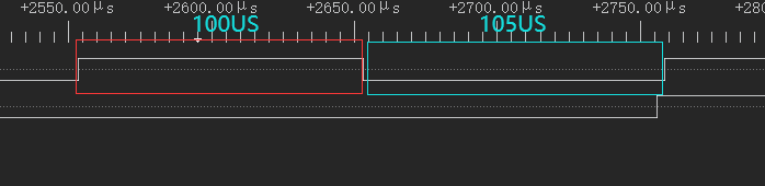
As shown in the figure, the duration of the last low-level of cfg data 3 is 105 us (not the 100 us set by cfg data 3). Therefore, with this usage method, after sending the first set of DMA data, re-triggering the DMA in the interrupt introduces a certain delay in the signal.
(2) PWM_CHAIN_DMA Experimental Results
Using chained DMA enables continuous transmission without MCU intervention. The linked list structure is as follows:
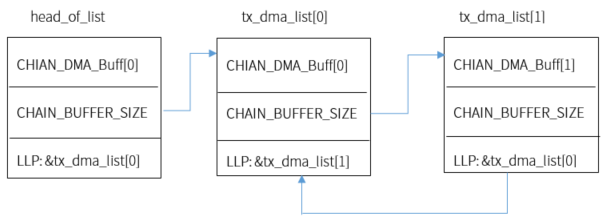
First, create the head node head_of_list, then add nodes to the circular linked list. As shown in the flowchart, execution starts with the head pointer, and then cycles through each node in sequence until the LLP is set to 0, at which point it stops.

A detailed explanation of the red box: there is no delay during the switching of cfg data between pointer 1 and pointer 2.
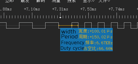
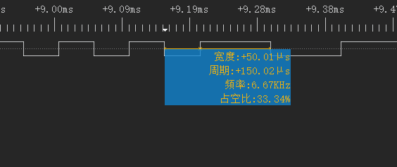
As shown in the figures, there is no delay. Therefore, using the linked-list approach allows continuous PWM waveforms to be generated.
Note
- In the interrupt, some DMA configurations need to be updated: source address update, DMA trigger, etc.
- In this mode, unlike IR FIFO mode, the interrupt is not triggered when the number of cfg data entries in the FIFO is empty, but rather when all PWM signal frames configured in the FIFO have been fully executed.
DMA Configuration Interface:
void pwm_set_dma_config(dma_chn_e chn);                                    // Configure DMA channel
void pwm_set_dma_buf(dma_chn_e chn, unsigned int buf_addr, unsigned int len);  // Set DMA buffer
void pwm_ir_dma_mode_start(dma_chn_e chn);                                 // Start DMA
DMA Linked List Configuration Interface (for chained DMA):
void pwm_set_dma_chain_llp(dma_chn_e chn, unsigned short *src_addr, unsigned int data_len, dma_chain_config_t *head_of_list);
void pwm_set_tx_dma_add_list_element(dma_chn_e chn, dma_chain_config_t *config_addr, dma_chain_config_t *llpoint, unsigned short *src_addr, unsigned int data_len);
Note
- When using chained DMA, the source address
src_addrmust be word-aligned (4 bytes); otherwise, the program enters an exception state.
Interrupts
The supported PWM interrupt settings are described below (the hardware does not automatically clear interrupt flags; they must be cleared manually by software).
Interrupts Supported by PWM0
| Interrupt Type | Description |
|---|---|
| FLD_PWM_FRAME_DONE_IRQ | Generated when each signal frame is completed |
| FLD_PWM0_PNUM_IRQ | Generated each time a pulse group is sent |
| FLD_PWM0_IR_FIFO_IRQ | Entered when the number of cfg data entries in the FIFO is less than (not including equal to) the configured value (trigger_level) |
| FLD_PWM0_IR_DMA_FIFO_IRQ | Entered after the FIFO finishes executing the cfg data sent by DMA |
Interrupts Supported by other channels
| Interrupt Type | Description |
|---|---|
| FLD_PWM_FRAME_DONE_IRQ | Generated when each signal frame is completed |
Note
- All other channels on all chips support only the "frame done" interrupt.
Interrupt Configuration Interface
TC series:
void pwm_set_interrupt_enable(PWM_IRQ irq);              // Enable PWM interrupt
void pwm_set_interrupt_disable(PWM_IRQ irq);             // Disable PWM interrupt
unsigned char pwm_get_interrupt_status(PWM_IRQ status);  // Get PWM interrupt status
void pwm_clear_interrupt_status(PWM_IRQ status);         // Clear PWM interrupt status
Note
- The TC series uses the
PWM_IRQenumeration for interrupt masks and states (e.g.,PWM_IRQ_PWM0_FRAME,PWM_IRQ_PWM0_PNUM,PWM_IRQ_PWM0_IR_FIFO,PWM_IRQ_PWM0_IR_DMA_FIFO_DONE), with the interrupt type for each channel listed separately (e.g.,PWM_IRQ_PWM1_FRAME,PWM_IRQ_PWM2_FRAME, etc.). Among these,PWM_IRQ_PWM0_IR_FIFOmust be configured via the separatereg_pwm0_fifo_mode_irq_maskandreg_pwm0_fifo_mode_irq_staregisters; the interface internally distinguishes between them.
TL series:
void pwm_set_irq_mask(pwm_irq_e mask);                  // Enable PWM interrupt mask
void pwm_clr_irq_mask(pwm_irq_e mask);                  // Disable PWM interrupt mask
unsigned char pwm_get_irq_status(pwm_irq_e status);     // Get PWM interrupt status
void pwm_clr_irq_status(pwm_irq_e status);              // Clear PWM interrupt status
TL322x:
void pwm_set_irq_mask(pwm_id_e id, pwm_irq_type_e type);     // Enable PWM interrupt mask
void pwm_clr_irq_mask(pwm_id_e id, pwm_irq_type_e type);     // Disable PWM interrupt mask
unsigned int pwm_get_irq_status(pwm_id_e id, pwm_irq_type_e type);  // Get PWM interrupt status
void pwm_clr_irq_status(pwm_id_e id, pwm_irq_type_e type);   // Clear PWM interrupt status
Interface Differences: The TC series uses pwm_set_interrupt_enable/disable + pwm_clear_interrupt_status (separate registers distinguish IR FIFO interrupts); The TL series uses pwm_set_irq_mask/clr_irq_mask + pwm_clr_irq_status; the TL322x requires an additional pwm_id_e channel parameter.
Note
- There is a delay of approximately 2 to 4 us when responding to an interrupt.
- In the interrupt handler, the interrupt flag should be cleared before processing the main task to prevent repeated interrupts.
IR FIFO Mode Trigger Level Configuration
The trigger_level value for IR FIFO mode can be configured via the following function interface:
static inline void pwm_set_pwm0_ir_fifo_irq_trig_level(unsigned char trig_level);
When the number of data entries in the FIFO falls below this value, an interrupt is triggered.
Notes
- Channel Differences: PWM0 supports all 5 modes, while PWM1~PWM23 only support continuous mode.
- 32kHz Clock Source: When using the 32kHz clock source, only continuous mode and counting mode are supported, and frequency division is not supported.
- DMA Address Alignment: When using the DMA function, the source address must be word-aligned (4 bytes); otherwise, the program enters an exception state.
- FIFO Depth: The depth of the IR FIFO is 8 bytes.
-
Duty Cycle Update:
- In continuous mode, updating the duty cycle takes effect in the next frame.
- In counting mode, modifying the duty cycle during transmission does not change the duty cycle.
- In IR mode, the duty cycle can be changed in between, but it takes effect after the current pulse group finishes executing.
-
Stop Behavior:
- In continuous mode and counting mode, stop immediately halts signal output.
- In IR FIFO mode, stop only halts the execution of the current cfg data without affecting the execution of subsequent cfg data in the FIFO.
-
Advanced Features: Advanced features such as center alignment and phase shift are supported only by certain chips; see the "Summary Table of Chip Feature Differences" in PWM Overview for details.
- 32kHz Clock Interrupt Delay: When using the 32kHz clock source, interrupts in continuous mode and counting mode trigger one 32kHz clock cycle earlier than expected. If an interrupt is required, it is recommended to implement it using a GPIO interrupt.
I2C
Introduction
I2C (Inter-Integrated Circuit) is a serial bus composed of the data line SDA and the clock line SCL. It can send and receive data and is a half-duplex communication method. The clock is controlled by the main device.
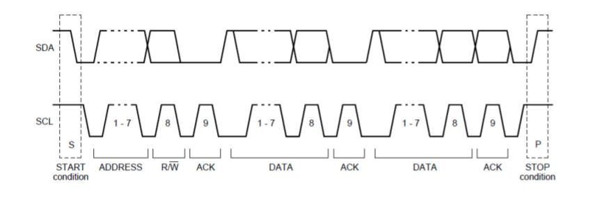
The detailed explanation of the I2C communication protocol is as follows:
| Status | Process |
|---|---|
| Idle state | When both the SDA and SCL signals of the I2C bus are at high levels, they are defined as the bus's idle state. |
| Start signal | During the SCL at a high level, the SDA jumps from high to low. |
| Stop signal | During the SCL at a high level, the SDA jumps from low to high. |
| Ackowledgement signal | The requirement for the feedback effective response bit ACK is: the receiver pulls the SDA signal low during the low level of the 9th clock pulse and maintains a stable low level during the high level of that clock. If the receiver is the master device, after receiving the last byte, it sends a NACK signal to notify the controlled transmitter to end data transmission and release the SDA signal, so the master device receiver can send a stop signal P. |
| Data validity | When the I2C bus is used for data transmission, the data on the data line must remain stable during high clock signals. Only when the signal on the clock line is at a low level is the high or low state on the data line allowed to change. |
| Data transmission | Each bit of data transmitted on the I2C bus has a corresponding clock pulse (or synchronization control), meaning each bit of data is transmitted bit by bit on the SDA with the help of the SCL serial clock. |
Chip overview
There are differences in design principles and interface packaging in I2C module between chips, classified as follows:
| Classification | Chips |
|---|---|
| Category 1 | B91/B92/TL751x/TL721x/TL321x/TL322x/TL323x |
| Category 2 | B85/B87/B80/B80B/TC321x/TC123x |
Note
B91 includes TLSR951x and TLSR921x, B92 includes TLSR952x and TLSR922x, B80 includes TLSR8208A/B/C/D and TLSR8373E/F, B80B includes TLSR8208E/F/G/H/J and TLSR8373A/B/C/FBR, B85 includes TLSR825x and TLSR8359, B87 includes TLSR827x and TLSR8355.
I2C in Category 1
| Chips | I2C module | Master/slave mode | DMA | Stretch |
|---|---|---|---|---|
| B91 | 1-channel I2C | Master + Slave | Support | Limited support |
| B92/TL751x/TL721x/TL321x | One i2c + one i2c1_m | i2c: master + slave, i2c1_m: master only | Support | Support |
| TL322x/TL323x | Dual I2C | i2c: Master + Slave | Support | Support |
I2C characteristics
B91
- GPIO pin selection is used for SDA/SCL
- Non-DMA and DMA data transmission modes
- Basic stretch functionality is supported
- DMA transmission length: Configured according to the negotiated length
Other chips with I2C characteristics
- GPIO pin selection is used for SDA/SCL
- Non-DMA and DMA data transmission modes
- Enhanced stretch functionality and interrupt support
- NACK detection during the ID and data phases
- DMA write_num function, used to report the length of received data.
- Maximum DMA transfer length: 0xFFFFFC bytes (B92), any length (except for other B92 chips)
Interrupt
I2C interrupts are used to notify the MCU of various communication events, including FIFO trigger, frame transfer completion, NACK detection, stretch status, and more. Different chips (B91, other chips) support different types of interrupts. This document details the trigger conditions and clearing methods for each interrupt.
Types of interrupts and trigger conditions
- B91 interrupts
| Interrupt | Trigger conditions | Automatic/manual clearing |
|---|---|---|
| I2C_TXDONE_STATUS | Triggered when a stop signal is detected | Manual clearing is required |
| I2C_TX_BUF_STATUS | TX FIFO Count < = tx_irq_trig_lev triggers | Automatically clearing |
| I2C_RXDONE_STATUS | Triggered when a stop signal is detected | Manual clearing is required |
| I2C_RX_BUF_STATUS | RX FIFO count > = i2c_rx_irq_trig_cnt triggered | Automatically clears after reading data |
- Other chip interrupts
| Interrupt | Trigger conditions | Automatic/manual clearing |
|---|---|---|
| I2C_SLAVE_WR_STATUS | Triggered when the device parses commands to the master device read/write commands | Manual clearing is required |
| I2C_MASTER_NAK_STATUS | Triggered when the main device detects NACK | Manual clearing is required |
| I2C_RX_BUF_STATUS | Triggers when RX FIFO count > = FLD_I2C_RX_IRQ_TRIG_LEV | Automatically clear, but manual clearing will reset the RX FIFO pointer |
| I2C_TX_BUF_STATUS | Triggers when TX FIFO count < = FLD_I2C_TX_IRQ_TRIG_LEV | Automatically clearing |
| I2C_RX_DONE_STATUS | Triggered when a stop signal is detected | Manual clearing is required |
| I2C_TX_DONE_STATUS | Triggered when a stop signal is detected | Manual clearing is required |
| I2C_RX_END_STATUS | Triggered when a frame of data is received (a stop signal has been sent) | Manual clearing is required |
| I2C_TX_END_STATUS | Triggered after sending a frame of data (stop signal sent) | Manual clearing is required |
| I2C_STRETCH_STATUS | With the Stretch function, triggers when TX FIFO is empty or RX FIFO is full | Manual clearing is required |
STRETCH function
Master: By default, Stretch is enabled. When SCL is pulled down, the master's hardware state machine is in the current state. Only after the SCL slave is released will the master's hardware state machine continue execution.
Slave end: Enables stretch functionality by calling the i2c_slave_stretch_en() API. When the slave rxfifo is full or txfifo is empty, SCL is triggered to pull down; if the trigger conditions are not met, SCL is automatically released.
Note
- For B91 chip, during the sending process of the i2c slave end, if stretch is enabled, once the i2c slave ends and the stretch condition is met, it remains held continuously. Manually closing after sending releases and restores it; Chips after B91 have no issues. When sending the i2c slave, there is a length check, and once the length is reached, the stretch is released.
- B91 Solution: The stretch function is always enabled. After configuring tx_dma, turn it off, then check the 'tx done' status on the I2C Slave end at the enabled area. If set to 1, enable it.
GPIO pin configuration
Pin options
void i2c_set_pin(gpio_func_pin_e sda_pin, gpio_func_pin_e scl_pin);
Pin configuration automatically completes the following operations:
- Enable input for SDA and SCL
- Configure a 10Kohm pull-up resistor
- Set mux function to I2C
- Disable GPIO function
I2C operating mode
The Telink I2C driver supports both master and slave operating modes, and supports both non-DMA (NDMA) and DMA data transmission modes. For the internal design mechanism of nodma/dma, refer to the Datasheet I2C chapter.
- I2C Master
a. Initialization and Configuration
NDMA/DMA General Initialization:
// 1. Initialize the SDA/SCL pins
i2c_set_pin(sda_pin, scl_pin);

// 2. Configure the I2C clock frequency
i2c_set_master_clk((unsigned char)(sys_clk.pclk * 1000 * 1000 / (4 * 400000)));

// 3. Enable the master device functions
i2c_master_init();
DMA Initialization:
//Configure the TX/RX DMA channels
i2c_set_tx_dma_config(DMA1);
i2c_set_rx_dma_config(DMA0);
b. Interrupt Configuration
| Mode | B91 interrupt configuration | Other chips interrupt configuration |
|---|---|---|
| NDMA writes | 'Polling method, no interrupt configuration required | 'Polling method, no interrupt configuration required |
| NDMA reads | 'Polling method, no interrupt configuration required | 'Polling method, no interrupt configuration required |
| DMA writes | No interrupt configuration required | i2c_set_irq_mask(I2C_MASTER_NAK_MASK) |
| DMA reads | No interrupt configuration required | i2c_set_irq_mask(I2C_MASTER_NAK_MASK) |
c. Interrupt Response (DMA NACK)
if (i2c_get_irq_status(I2C_MASTER_NAK_STATUS)) {
    i2c_clr_irq_status(I2C_MASTER_NAK_STATUS);
    reg_i2c_sct1 = FLD_I2C_LS_STOP;
    while (i2c_master_busy());
    dma_chn_dis(I2C_TX_DMA_CHN);

    if (I2C_MASTER_WRITE == i2c_get_master_wr_status()) {
        i2c_clr_irq_status(I2C_TX_BUF_STATUS);
    }
}
d. Data Transmission and Reception
NDMA Mode:
//Main Device Writing (Polling)
unsigned char ret = i2c_master_write(0x5a, tx_data, len);
//ret = 0: ID or data stage receives NACK
//ret = 1: Write successfully
//ret = DRV_API_TIMEOUT: Timeout returns

//Master device reading (polling)
unsigned char ret = i2c_master_read(0x5a, rx_data, len);
DMA Mode:
//Master device DMA writes
i2c_master_write_dma(0x5a, tx_data, len);
while (i2c_master_busy());

//Master device DMA reads
i2c_master_read_dma(0x5a, rx_data, len);
while (i2c_master_busy());
Note
- B91: Only the ID detection phase; if NCA is detected, a stop signal is sent and the current operation is terminated.
- Other chips: Supports NACK detection at both the ID and data stages in both NDMA and DMA modes. If NACK is detected, a stop signal is sent and the current operation is suspended.
- Slave Mode Initialization
a. Slave NDMA mode
In non-DMA mode from slave devices, the MCU reads and writes data byte by byte directly through I2C data registers. When receiving data, an interrupt method is usually used, with the RX FIFO triggering level interrupt and frame-end interrupt working together to complete the reception of a single frame.
Initialization and configuration:
// 1. Initialize the SDA/SCL pins
i2c_set_pin(sda_pin, scl_pin);

// 2. Enable slave device functions and set IDs
i2c_slave_init(0x5a);
Interrupt configuration:
Slave write (Master Reads Slave Device)
| Chips | Stretch | Interrupt configuration |
|---|---|---|
| B91 | No supported | No related interrupts, data must be filled in in advance |
| Other chips | Not used | No related interrupts, data must be filled in in advance |
| Other chips | Used | i2c_set_irq_mask(I2C_SLAVE_WR_MASK) |
Read from Slave device (Master writes to slave device)
| Chips | Interrupt configuration |
|---|---|
| B91 | i2c_rx_irq_trig_cnt() + i2c_set_irq_mask(I2C_RX_BUF_MASK \| I2C_RX_DONE_MASK) |
| Other chips | i2c_rx_irq_trig_cnt() + i2c_set_irq_mask(I2C_RX_BUF_MASK | I2C_RX_END_MASK) |
Data transmission and reception:
Slave writes (Responds to Master Device Read)
Not using Stretch:
//Data must be pre-filled before the master device sends the read command
i2c_slave_write(tx_data, len);
//FIFO is only 8 bytes long and requires advance preparation
Using Stretch (other chips):
//Fill the data in I2C_SLAVE_WR_MASK interrupts
void i2c_irq_handler(void)
{
    if (i2c_get_irq_status(I2C_SLAVE_WR_STATUS)) {
        i2c_clr_irq_status(I2C_SLAVE_WR_STATUS);
        if (I2C_SLAVE_WRITE == i2c_slave_get_cmd()) {
            i2c_slave_write(tx_data, len);
        }
    }
}
Key points for using Stretch: When a slave device uses the Stretch feature, use I2C_SLAVE_WR_MASK interrupts to determine when the master device reads data and then fill in the data. When the slave device does not use the Stretch function, if the I2C_SLAVE_WR_MASK interrupt is used to determine the master device's read timing, the MCU may not have time to handle it, so data must be pre-filled before the master device reads.
Read from Slave device (Response to Master Device Writes)
B91 Interrupt Handling:
#define SLAVE_RX_IRQ_TRIG_LEVEL 4

i2c_rx_irq_trig_cnt(SLAVE_RX_IRQ_TRIG_LEVEL);
i2c_set_irq_mask(I2C_RX_BUF_MASK | I2C_RX_DONE_MASK);

void i2c_irq_handler(void)
{
    if (i2c_get_irq_status(I2C_RX_BUF_STATUS)) {
        i2c_slave_read(rx_buff + offset, SLAVE_RX_IRQ_TRIG_LEVEL);
        offset += SLAVE_RX_IRQ_TRIG_LEVEL;
    }
    if (i2c_get_irq_status(I2C_RXDONE_STATUS)) {
        if (remaining_len > 0) {
            i2c_slave_read(rx_buff + offset, remaining_len);
        }
        i2c_clr_fifo(I2C_RX_BUFF_CLR);
        rx_done_flag = 1;
    }
}
Other chip interrupt handling:
#define SLAVE_RX_IRQ_TRIG_LEVEL 4

i2c_rx_irq_trig_cnt(SLAVE_RX_IRQ_TRIG_LEVEL);
i2c_set_irq_mask(I2C_RX_BUF_MASK | I2C_RX_END_MASK);

void i2c_irq_handler(void)
{
    if (i2c_get_irq_status(I2C_RX_BUF_STATUS)) {
        i2c_slave_read(rx_buff + offset, SLAVE_RX_IRQ_TRIG_LEVEL);
        offset += SLAVE_RX_IRQ_TRIG_LEVEL;
    }
    if (i2c_get_irq_status(I2C_RX_END_STATUS)) {
        i2c_clr_irq_status(I2C_RX_END_STATUS);
        if (i2c_get_rx_buf_cnt() > 0) {
            i2c_slave_read(rx_buff + offset, i2c_get_rx_buf_cnt());
        }
        offset = 0;
        rx_done_flag = 1;
    }
}
Data transmission and reception (Precautions):
- When writing from the B91 slave device, the FIFO size is only 8 bytes, requiring data to be pre-filled before the master device reads.
- Other chips that do not use Stretch also need to pre-fill data; When using Stretch, you can dynamically fill
I2C_SLAVE_WR_MASKinterrupts. i2c_rx_irq_trig_cnt()is recommended to be set to 1 or 4, with a range less than 8.
b. Slave DMA mode
In Device DMA mode, the DMA controller automatically transfers data from memory to the I2C TX FIFO (responds to the master device read) or from the I2C RX FIFO to memory (responds to the master device write).
Initialization and configuration:
// 1. Initialize the SDA/SCL pins
i2c_set_pin(sda_pin, scl_pin);

// 2. Enable slave device functions and set IDs
i2c_slave_init(0x5a);

// 3. Configure DMA channels
i2c_set_tx_dma_config(DMA1);
i2c_set_rx_dma_config(DMA0);
Interrupt configuration:
Slave device DMA write (Response to Master Device Read)
| Chips | Stretch | Interrupt configuration |
|---|---|---|
| B91 | No supported | i2c_set_irq_mask (I2C_TX_DONE_MASK) (Clear before use I2C_TX_DONE_CLR) |
| Other chips | Not used | i2c_set_irq_mask(I2C_TX_END_MASK) |
| Other chips | Used | i2c_set_irq_mask(I2C_SLAVE_WR_MASK) |
Slave device DMA read (Response to Master Device Write)
| Chips | Interrupt configuration |
|---|---|
| B91 | dma_set_irq_mask(TC_MASK) |
| Other chips | dma_set_irq_mask (TC_MASK) or i2c_set_irq_mask (I2C_RX_END_MASK). |
Data Transmission and Reception:
Slave Device DMA write (Response to Master Device Read)
B91:
//Clear the TX_DONE state during initialization
i2c_clr_irq_status(I2C_TX_DONE_CLR);
i2c_set_irq_mask(I2C_TX_DONE_MASK);

//Configure DMA to write data
i2c_slave_set_tx_dma(tx_data, len);

//Interrupt handling
void i2c_irq_handler(void)
{
    if (i2c_get_irq_status(I2C_TXDONE_STATUS)) {
        i2c_clr_irq_status(I2C_TX_DONE_CLR);
        //Configure the next TX DMA
    }
}
Other chips use Stretch:
i2c_slave_stretch_en();
i2c_set_irq_mask(I2C_SLAVE_WR_MASK);

void i2c_irq_handler(void)
{
    if (i2c_get_irq_status(I2C_SLAVE_WR_STATUS)) {
        i2c_clr_irq_status(I2C_SLAVE_WR_STATUS);
        if (I2C_SLAVE_WRITE == i2c_slave_get_cmd()) {
            i2c_slave_set_tx_dma(tx_data, len);
        }
    }
}
Read from Slave device DMA (Respond to Master Device Write)
B91:
//Configure DMA to read data
i2c_slave_set_rx_dma(rx_data, len);

//Completed through DMA TC interrupt judgment
dma_set_irq_mask(TC_MASK);

//Interrupt handling
void dma_irq_handler(void)
{
    if (dma_get_tc_irq_status(I2C_RX_DMA_STATUS)) {
        dma_clr_tc_irq_status(I2C_RX_DMA_STATUS);
        //Configure the next RX DMA
    }
}
Other chips
//Configure DMA to read data
i2c_slave_set_rx_dma(rx_data + 4, DMA_REV_LEN);

//Method 1: Via DMA TC interrupt
dma_set_irq_mask(TC_MASK);

//Method 2: Via I2C_RX_END_MASK interrupt
i2c_set_irq_mask(I2C_RX_END_MASK);

void i2c_irq_handler(void)
{
    if (i2c_get_irq_status(I2C_RX_END_STATUS)) {
        i2c_clr_irq_status(I2C_RX_END_STATUS);
        //Configure the next RX DMA
        i2c_slave_set_rx_dma(rx_data + 4, DMA_REV_LEN);
    }
}
Note
- The buff data buffer must be aligned by word (4 bytes).
- Before using the
I2C_TX_DONE_MASKon the B91 chips, manually clearthe I2C_TX_DONE_CLR, otherwise it keeps interrupting. I2C_TX_DONE_MASKOnly indicates that the data part has been sent, excluding the stop signal; Other chips are recommended to useI2C_TX_END_MASK- Except for the B91 chip, the DMA read time received is written to the first 4 bytes of the buffer. The read buffer size is
BUFF_DATA_LEN_DMA + 4, with the first 4 bytes storing the actual receive length.
- I2C1_M Module (Master mode only, NDMA only)
a. Initialization and Configuration
// 1. Initialize the SDA/SCL pins
i2c1_m_set_pin(sda_pin, scl_pin);

// 2. Configure the I2C clock frequency
i2c1_m_set_master_clk((unsigned char)(sys_clk.pclk * 1000 * 1000 / (4 * 100000)));

// 3. Enable the master device functions
i2c1_m_master_init();
b. Data Transmission and Reception
//i2c1_m Write (can include an address, put the address into txbuff and send it together as data)
i2c1_m_master_write(0x5a, tx_data, len);

//i2c1_m Read
i2c1_m_master_read(0x5a, rx_data, len);

//i2c1_m Read after writing
i2c1_m_master_write_read(0x5a, wr_data, wr_len, rd_data, rd_len);
DEMO Description
- Hardware connection
When testing I2C communication with two boards:
| Master Device | Slave Device |
|---|---|
| SCL | SCL |
| SDA | SDA |
| GND | GND |
Important:
- Power on slave devices first, then power on master devices (to avoid data errors)
-
There must be a common-ground connection between the two boards.
-
NODMA
a. Configure Macros
#define I2C_MASTER_DEVICE 1  // i2c master demo
#define I2C_SLAVE_DEVICE  2  // i2c slave demo
#define I2C_DEVICE I2C_SLAVE_DEVICE // Select the master or slave device

#if !defined(MCU_CORE_B91)
    #define I2C_STRETCH_EN   0
    #define I2C_STRETCH_DIS  1
    #define I2C_STRETCH_MODE I2C_STRETCH_EN // Select Stretch mode
#endif

#define I2C_CLK_SPEED 400,000 // I2C clock 400K
#define SLAVE_RX_IRQ_TRIG_LEVEL 4 // Slave device RX interrupt trigger level
#define BUFF_DATA_LEN_NO_DMA 32 // data buffer length
b. Test Description
Master Device
( I2C_DEVICE I2C_MASTER_DEVICE)
Data Flow:
Burn the bin file to the master device
The master writes data to the slave and then reads the data back
Compare whether the data written and read back are consistent
Slave Device
(I2C_DEVICE I2C_SLAVE_DEVICE)
Data Flow:
Burn the bin file to the slave device
Do not use Stretch(I2C_STRETCH_MODE I2C_STRETCH_DIS):
Receive data from the master device and then write the received data back to the master device
Using Stretch (except for B91 chips) (I2C_STRETCH_MODE I2C_STRETCH_EN):
Another communication mechanism with the master device is to receive data from the device and write it back to the master device.
- DMA
a. Configure Macros
#define I2C_TX_DMA_CHN DMA1
#define I2C_RX_DMA_CHN DMA0

#define I2C_MASTER_DEVICE 1
#define I2C_SLAVE_DEVICE  2
#define I2C_DEVICE        I2C_MASTER_DEVICE

#if (I2C_DEVICE == I2C_MASTER_DEVICE)
    #define I2C_CLK_SPEED 200,000 // I2C clock 200K
    #define BUFF_DATA_LEN_DMA 32
##elif (I2C_DEVICE == I2C_SLAVE_DEVICE)
    #if !defined(MCU_CORE_B91)
        #define I2C_STRETCH_EN   1
        #define I2C_STRETCH_DIS  2
        #define I2C_STRETCH_MODE I2C_STRETCH_EN
    #endif
    #define BUFF_DATA_LEN_DMA 32

    //B91: DMA_REV_LEN Matches the transmission length
    //B92: DMA_REV_LEN can be set to maximum value 0xFFFFFC and enable write_num
    //Chips other than B91/B92: DMA_REV_LEN is any 4-byte alignment length
    #if defined(MCU_CORE_B91)
        #define DMA_REV_LEN BUFF_DATA_LEN_DMA
    #elif defined(MCU_CORE_B92)
        #define DMA_REV_LEN 0xFFFFFC
    #else
        #define DMA_REV_LEN 32
    #endif
#endif
b. Test Instructions
Master Device Data Stream:
( I2C_DEVICE I2C_MASTER_DEVICE)
- Burn the bin file to the master device.
- The master writes data to the slave and then reads the data back.
- Compare whether the data written and read back are consistent.
Slave Device data stream:
(I2C_DEVICE I2C_SLAVE_DEVICE)
- Dot using Stretch (I2C_STRETCH_MODE I2C_STRETCH_DIS): Receive data from the master device and then write the received data back to the master device (pre-configure rxdma, configure tx dma in rx dma, configure rxdma in tx interrupt; demo alternates configuration like this)
-
Use Stretch (except for B91 chips) (I2C_STRETCH_MODE I2C_STRETCH_EN): After receiving data from the device, write it back to the master device.
-
Test results
Using a logic analyzer to capture timing:
Channel 0: SCL signal
Channel 1: SDA signal
Channel 2: LED2 (error indicator)
Master device sends data:

Master device receives data:

Special Note
- During I2C write operations, the slave responds to ACK after the master device writes the last byte, and then the master sends a stop signal to end the communication.
I2C module in Category 2
The 8 Series (B85m) I2C module differs significantly from the 9 Series: the 8 Series does not have a true DMA transmission mode. Data transmission on the master side is handled by sequential read/write registers on the MCU, while the slave side is automatically parsed by hardware on the bus, so the MCU does not need to participate byte by byte.
Chip Overview and Features
Main features:
- GPIO pins can be configured for SDA/SCL, with internal pins enabling input and pull-up 10Kohm.
- Supports both Master and Slave modes
- The Slave side supports two data organization modes: MAPPING mode and DMA mode (Note: DMA mode names are historical and are not actual DMA transmissions; see the Slave mode operation description for details).
- Master data transmission is fully controlled sequentially by the MCU (no DMA)
- Data transmission and reception on the Slave end are automatically completed by hardware; the MCU only needs to detect read/write events during interrupts.
- Supports Slave ID phase interrupts (triggered when master device read/write commands arrive)
- Supports single-byte, double-byte, and three-byte address access (AddrLen 0/1/2/3)
- Maximum Speed: Hardware tests can stably support up to 1 Mbps (higher speeds depend on hardware environment, no further verification conducted)
Interrupt
The 8 Series I2C only generates interrupts at the slave end, which notify the MCU master device of read/write operations initiated by it. The types of interrupts are as follows:
| Interrupt | Trigger conditions | Clearing methods |
|---|---|---|
| HOST_CMD_IRQ | Triggered when the master device initiates a read or write command (ID resolution complete). | Manually clear the write status registers |
| HOST_READ_IRQ | Triggered only when the master device initiates a read command | Manually clear the write status registers |
Explanation:
- Both read/write events trigger
HOST_CMD_IRQ, and read events setHOST_READ_IRQ, so during interrupts, read or write can be distinguished byHOST_READ_IRQ. - Both status bits must be cleared together after processing (write register value to clear).
- To enable interrupts, open the I2C hybrid command interrupt via
irq_set_mask(FLD_IRQ_MIX_CMD_EN) and then callirq_enable().
Related Interfaces:
//Obtain interrupt status
unsigned char i2c_get_interrupt_status(i2c_irq_e irq_status);

//Clear the interrupt status
void i2c_clear_interrupt_status(i2c_irq_e irq_status);
GPIO pin configuration
8 Series uses i2c_gpio_set() to configure SDA/SCL pins, with the function completing it internally:
- Enable SDA / SCL pin inputs
- Configure a 10Kohm pull-up resistor
- Set the mux function to I2C
- Disable the corresponding GPIO function
void i2c_gpio_set(GPIO_PinTypeDef sda_pin, GPIO_PinTypeDef scl_pin);
The B85 uses a single-parameter i2c_gpio_set (I2C_GPIO_SDA_SCL) format, while other chips use a dual-parameter form.
I2C operating mode
Working Modes: MAPPING mode and DMA mode. The working mechanism is introduced as follows:
I2C_MAPPING_MODE:
Slave: Defines a receiving buff and writes the buff's address to the register;
Master: No address information is needed when sending data; the slave side stores the data sent by the master in a defined buff address
When the Master side reads data, it does not need to send address information; the slave side sends data from the defined Buff address
This mode has a usage requirement: the buff defined on the slave side must be 128 bytes aligned, and the 128 addresses can be written freely, but when reading, only the last 64 bytes can be read:
128 bytes aligned
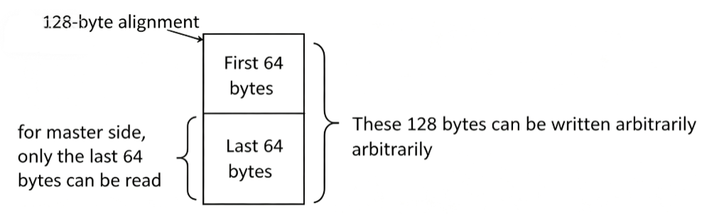
Therefore, to ensure that what is written and read are consistent, the address information passed to the slave register is:
i2c_slave_init(0x5C,I2C_SLAVE_MAP,(unsignedchar*)i2c_slave_mapping_buff+64); Store the buff address of the i2c slave into the following register. When the master side reads or writes, the slave store or read data from the address information stored in this register:
Note
- Although the master side can only read the last 64 bytes, the slave side can freely access these 128 bytes.
I2C_DMA_MODE: Although it is called DMA mode, it is actually not DMA transmission.
- Slave: No need to define receiving buffs
-
Master: When sending and receiving, the master needs to send address information, then the slave side parses the address sent from the master, and the received data is stored at that address, or the contents of that address are sent to the master.
-
Master mode
Initialization and Configuration:
// 1. Configure SDA/SCL pins
i2c_gpio_set(I2C_GPIO_SDA, I2C_GPIO_SCL);

// 2. Master device initialization: Set the Slave ID and clock frequency division
//The lowest bit of a slaveID is the read/write bit (R:High W:Low), for example, 0x5C is written as 0x5C and read as 0x5D
//    DivClock = CLOCK_SYS_CLOCK_HZ / (4 * I2C_CLK_SPEED)
i2c_master_init(0x5C, (unsigned char)(CLOCK_SYS_CLOCK_HZ / (4 * I2C_CLK_SPEED)));
Data transceiver interface (MCU sequential control, non-DMA):
| Interface | Purpose |
|---|---|
i2c_write_series(Addr, AddrLen, dataBuf, dataLen) |
Write a piece of data to a specified address |
i2c_read_series(Addr, AddrLen, dataBuf, dataLen) |
Read a piece of data from a specified address |
Parameter Description:
Addr: The internal register/SRAM address of the slave corresponds to the address phase in the master sequenceAddrLen: Address length, 0/1/2/3 bytes- 0: MAPPING mode does not require a sending address
- 1/2/3: Send 1/2/3 byte addresses
dataBuf: Data bufferdataLen: Data length (bytes)
Write sequence
start + device_id(W) + [addr(0/1/2/3 byte)] + data(1..n byte) + stop
Read sequence
start + device_id(W) + [addr(0/1/2/3 byte)] + restart + device_id(R) + data(1..n byte) + stop
Example of master usage in MAPPING mode:
//In MAPPING mode, AddrLen=0 is not required, no sending address required
i2c_write_series(0, 0, (unsigned char *)i2c_tx_buff, BUFF_DATA_LEN);
i2c_read_series(0, 0, (unsigned char *)i2c_rx_buff, BUFF_DATA_LEN);
Example of master usage in DMA mode:
//Needs to send the internal SRAM address of the slave (3 bytes)
#define SLAVE_DEVICE_ADDR      0x48000
#define SLAVE_DEVICE_ADDR_LEN  3
i2c_write_series(SLAVE_DEVICE_ADDR, SLAVE_DEVICE_ADDR_LEN, (unsigned char *)i2c_tx_buff, BUFF_DATA_LEN);
i2c_read_series(SLAVE_DEVICE_ADDR,  SLAVE_DEVICE_ADDR_LEN, (unsigned char *)i2c_rx_buff, BUFF_DATA_LEN);
- Slave mode
a. MAPPING mode
Principle:
- The slave end defines a 128-byte aligned buffer in SRAM and writes this buffer address to the hardware register:
- buffer must be aligned at 128 bytes
- Within 128 bytes, the master can be written arbitrarily, but only the last 64 bytes of the master can be read.
- To ensure the master writes and reads the same data, the address passed in during slave initialization must be offset by +64:
In MAPPING mode, data on the slave side is automatically transferred by hardware, without the need for MCU byte processing.
b. SDMA mode
Explanation:
The "DMA mode" here is a historical name, is not actually a true DMA transmission. Essentially, the slave side automatically parses the data storage location based on the address field sent by the master (any SRAM address, address 3 bytes).
i2c_gpio_set(I2C_GPIO_SDA, I2C_GPIO_SCL);

//slave initialization: DMA mode, no buffer input required (pMapBuf passes 0)
i2c_slave_init(0x5C, I2C_SLAVE_DMA, 0);
Note
- The master side must send a 3-byte address (AddrLen=3) to specify the target location in the slave SRAM.
- The slave side does not need to define a receive buffer; hardware directly parses addresses and stores/reads SRAM data.
Demo explanation
Demo path: demo/vendor/I2C_Demo, switch working modes using the I2C_MODE macro in app_config.h:
#define I2C_DMA_MODE     1
#define I2C_MAPPING_MODE 2
#define I2C_MODE 1 // Choose 1 (DMA) or 2 (MAPPING)
And use I2C_DEVICE macros to choose whether to compile as master or slave:
#define I2C_MASTER_DEVICE  1
#define I2C_SLAVE_DEVICE    2
#define I2C_DEVICE          I2C_MASTER_DEVICE
(1) Hardware connection
| Master Device | Slave Device |
|---|---|
| SCL | SCL |
| SDA | SDA |
| GND | GND |
Important:
Power on the slave device first, then power on the master device (to avoid data errors); The two boards must be on the same ground.
(2) MAPPING mode test instructions
- Master Data Stream: Programme the master firmware → periodically writes data to the slave and then reads back → to compare whether the write and read data are consistent (the demo uses
i2c_tx_buff[0]++to auto-increment checks). - Slave Data Stream: Programme the slave firmware → receiving master device data and storing it in
i2c_slave_mapping_buff→ When the master device reads, the slave automatically returns data from the buffer. - Interrupts are only used to count read/write counts and flip LED indicators; data handling is entirely hardware-controlled.
(3) DMA Mode Test Instructions
- Master Data Stream: Programme master firmware → accessing the slave SRAM via
i2c_write_series/i2c_read_series0x48000 starting at 16 bytes→ periodically writes and reads back for comparison. - Slave Data Stream: Records the master's read/write counts during the → interrupt of the slave firmware and flips the LED. The data storage location is specified by the master at the address stage.
UART
UART Hardware Architecture
Overview of UART
UART (Universal Asynchronous Receiver/Transmitter) is an asynchronous, full-duplex serial communication protocol consisting of two data lines: Tx and Rx. Since there is no dedicated clock reference signal, both communicating parties must agree on the baud rate, data width, parity, and stop bits to operate at the same data rate.
The UART module provides the following capabilities:
| Feature | Description |
|---|---|
| Operating Mode | NDMA / DMA / DMA LLP |
| Hardware Flow | CTS (Clear to Send) / RTS (Request to Send) |
| FIFO Depth | 8 bytes each for TX FIFO and RX FIFO |
| Data Width | 8 bits |
| Stop Bits | 1 / 1.5 / 2 |
| Parity | None / Even / Odd |
| Single-Wire Mode | RTX pin (shared TX/RX on a single pin, used for S7816) |
Data Communication Timing
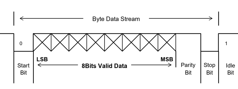
UART asynchronous communication transmits data one character (frame) at a time. Each character consists of:
| Bit Segment | Description |
|---|---|
| Start Bit | Logic 0, active low, marks the beginning of a character |
| Data Bits | 8 bits of logic 0 or 1, transmitted LSB-first |
| Parity Bit | Optional; makes the total number of 1 bits even or odd |
| Stop Bit(s) | Logic 1, 1 / 1.5 / 2 bits; longer stop bits improve tolerance |
| Idle | Logic 1, indicates the line is free |
Communication Principle
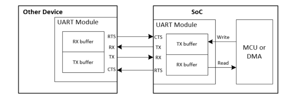
Taking the UART module in a Telink SoC as an example:
- Transmit path: Data is written by the MCU or DMA to the TX buffer (TX FIFO); the UART module serializes and sends the data over the TX pin to the peer device.
- Receive path: The peer device sends data that arrives on the RX pin; data is written into the RX buffer (RX FIFO), then read by the MCU or DMA.
Hardware flow control mechanism:
- When the chip's RX buffer is close to overflowing, it asserts the RTS pin to signal the peer to stop transmitting.
- When the chip detects an active signal on the CTS pin, it means the peer's RX buffer is close to overflowing, and the chip must stop transmitting.
Wiring note: Connect the local TX to the peer's RX, and the local RX to the peer's TX: TX <-> RX, RX <-> TX.
Chips Supported
Due to certain differences in chip design, there are various corresponding interface packaging configurations, which are classified as follows:
| Category | Chips |
|---|---|
| Category 1 | B91 / B92 / TL751x / TL721x / TL321x / TL322x / TL323x |
| Category 2 | B85 / B87 / B80 / B80B / TC321x / TC123x |
Note
- B91 includes TLSR951x and TLSR921x, B92 includes TLSR952x and TLSR922x, B80 includes TLSR8208A/B/C/D and TLSR8373E/F, B80B includes TLSR8208E/F/G/H/J and TLSR8373A/B/C/FBR, B85 includes TLSR825x and TLSR8359, B87 includes TLSR827x and TLSR8355.
UART Timeout Mechanism
| Chip series | Timeout Mechanism Calculation |
|---|---|
| Category 1 (B91 / B92), Category 2 | rx_timeout = ((bwpc+1) * bit_cnt) * mul |
| Category 1 (chips other than B91/B92) | rx_timeout = (((bwpc+1) * bit_cnt) * mul) * 2^n (n<=255) |
in which, the maximum of (bwpc+1) * bit_cnt can be set to 0xff.
The timeout period is calculated starting from the current byte. If no subsequent byte is received by the time the configured timeout period expires, the packet is considered fully received, and a timeout interrupt is generated.
RX Timeout Settings:
uart_set_rx_timeout(uart_num, bwpc, bit_cnt, mul);
bwpc: bit width, calculated fromuart_cal_div_and_bwpc().bit_cnt: The total number of bits required to transmit one byte (e.g., 1 start bit + 8 data bits + 1 parity bit + 2 stop bits = 12)mul: Timeout multiplier:UART_BW_MUL1= 1 byte time,UART_BW_MUL2= 2 byte times
Timeout = (1 / baud rate) × bit_cnt × mul. If no data is received within this time, a UART_RXDONE interrupt is generated.
Note
- When should the timeout value be adjusted? If a client sends a single transaction but there are time intervals within that transaction, and you want those intervals to be treated as part of the same transaction, you need to increase the timeout value. However, increasing the timeout value may cause two separate transactions to be treated as one, so the specific value must be determined based on the application scenario.
Work Mechanism of Internal FIFO
The UART FIFO has a depth of 8 bytes, and its status is reflected by the following counters:
| Counter | Direction | Description | Enquiry API |
|---|---|---|---|
rx_bufcnt |
RX | Increment by 1 for every byte received; decrement by 1 for every byte read | uart_get_rxfifo_num() |
tx_bufcnt |
TX | Increment by 1 for every byte written; decrement by 1 for every byte sent | uart_get_txfifo_num() |
rbcnt |
RX | Increment by 1 for every 1 byte read (FLD_UART_RBCNT) |
- |
wbcnt |
TX | Increment by 1 for every 1 byte written (FLD_UART_WBCNT) |
- |
UART in Category 1
Chip Difference
Different chips provide different quantity of UART; when using them, you must select the corresponding UART number (uart_num_e) based on the chip model:
| Chip series | UART Quantity | Available Numbers |
|---|---|---|
| B91 / B92 | 2 | UART0、UART1 |
| TL721x / TL321x | 3 | UART0、UART1、UART2 |
| TL7518 / TL751x | 4 | UART0 ~ UART3 |
| TL322x / TL323x | 5 | UART0 ~ UART4 |
UART Interrupt
(1) Overview of UART Interrupt
| Interrupt name | Assigned module | Trigger conditions | Clearing methods | Applicable modes |
|---|---|---|---|---|
UART_TXDONE |
UART | TX FIFO is empty, indicating that one frame of data is sent completely | Manual clearing | NDMA / DMA |
UART_RXDONE |
UART | If the RX timeout and no data is received, it means the frame of data has been received | Manual clearing | NDMA |
UART_RXBUF_IRQ_STATUS |
UART | Data volume in RX FIFOs ≥uart_rx_irq_trig_level sets thresholds |
Automatically clearing | NDMA |
UART_TXBUF_IRQ_STATUS |
UART | Data volume in TX FIFOs ≤uart_tx_irq_trig_level sets thresholds |
Automatically clearing | NDMA |
UART_RX_ERR |
UART | Received data errors (parity errors, stop bit errors, etc.) | Manual clearing | NDMA / DMA |
DMA TC(RX) |
DMA | DMA RX received length reaches the configured length | Manual clearing | DMA / DMA LLP |
(2) Interrupt mask configuration
Mask configuration API for each interrupt:
//NDMA mode: RX interrupt + error interrupt (UART module interrupt)
uart_set_irq_mask(UART0, UART_RX_IRQ_MASK | UART_ERR_IRQ_MASK);

//DMA Mode: TX_DONE + RX_DONE (UART module interrupted)
uart_set_irq_mask(UART0, UART_TXDONE_MASK | UART_RXDONE_MASK);

//DMA Mode: Use DMA TC interrupts (alternative to RX_DONE, which is a DMA module interrupt)
dma_set_irq_mask(UART_DMA_CHANNEL_RX, TC_MASK);

//DMA LLP Mode: Use DMA TC interrupts
dma_set_llp_irq_mode(UART_DMA_CHANNEL_RX, DMA_INTERRUPT_MODE);
dma_set_irq_mask(UART_DMA_CHANNEL_RX, TC_MASK);
Interrupt mask enumeration (uart_irq_mask_e):
| Mask name | Description |
|---|---|
UART_RX_IRQ_MASK |
Enable RXBUF_IRQ interrupt |
UART_TX_IRQ_MASK |
Enable TXBUF_IRQ interrupt |
UART_RXDONE_MASK |
Enable RXDONE interrupt |
UART_TXDONE_MASK |
Enable TXDONE interrupt |
UART_ERR_IRQ_MASK |
Enable RX_ERR interrupt |
(3) Interrupt status query and clear
B91 Enumeration of interrupt states (uart_irq_status_e):
| State name | Inquiry method | Clearing methods |
|---|---|---|
UART_TXDONE |
uart_get_irq_status(uart_num, UART_TXDONE) |
uart_clr_tx_done(uart_num) |
UART_RX_ERR |
uart_get_irq_status(uart_num, UART_RX_ERR) |
uart_clr_irq_status(uart_num, UART_CLR_RX) |
UART_RXBUF_IRQ_STATUS |
uart_get_irq_status(uart_num, UART_RXBUF_IRQ_STATUS) |
Automatically clears after reading FIFO |
UART_TXBUF_IRQ_STATUS |
uart_get_irq_status(uart_num, UART_TXBUF_IRQ_STATUS) |
Automatically clearing |
B92 and subsequent chip interrupt state enumeration (uart_irq_status_e):
| State name | Inquiry method | Clearing methods |
|---|---|---|
UART_TXDONE_IRQ_STATUS |
uart_get_irq_status(uart_num, UART_TXDONE_IRQ_STATUS) |
uart_clr_irq_status(uart_num, UART_TXDONE_IRQ_STATUS) |
UART_RXDONE_IRQ_STATUS |
uart_get_irq_status(uart_num, UART_RXDONE_IRQ_STATUS) |
uart_clr_irq_status(uart_num, UART_RXDONE_IRQ_STATUS) |
UART_RX_ERR |
uart_get_irq_status(uart_num, UART_RX_ERR) |
uart_clr_irq_status(uart_num, UART_RXBUF_IRQ_STATUS) |
UART_RXBUF_IRQ_STATUS |
uart_get_irq_status(uart_num, UART_RXBUF_IRQ_STATUS) |
uart_clr_irq_status(uart_num, UART_RXBUF_IRQ_STATUS) |
UART_TXBUF_IRQ_STATUS |
uart_get_irq_status(uart_num, UART_TXBUF_IRQ_STATUS) |
Automatically clearing |
(4) Chip differences
- UART_TXDONE: B91 has a default value of 1 and must be manually cleared during initialization; Other chips default to 0, so manual clearance is not required during initialization.
- UART_RXDONE: B91 only triggers in DMA mode, not NDMA, and only serves to clear RXDONE; Other chips support it, and when clearing RXDONE, it also serves as a clearing RXFIFO.
- UART_RXBUF_IRQ: When clearing FIFO, B91 When there is data in the FIFO, clearing the FIFO only deletes the contents of the FIFO; the pointer of the FIFO does not change; When data is in the FIFO on other chips, clearing the FIFO also clears the pointer to the FIFO's starting address. When there is no data in the FIFO, all chips clear the FIFO pointer and point to the FIFO's starting address.
Iterative optimization of UART DMA functionality
B91: The DMA write num function cannot be used and has no hardware writeback length, resulting in the only option to manually calculate the received data length during the RXDONE interrupt.
The above working mechanism can have the following scenarios: if two packets are very close together but an RXDONE interrupt occurs, but the next data entry has already arrived when processing the previous interrupt, clearing the previous interrupt status bit clears the next data entry, causing packet loss. If the customer cannot accept the lost packet, the recommended solution is that the time for both packets to exceed the interrupt processing time.
B92: Improvements have been made to address this issue, but when the write num function is enabled, the DMA receive length must be set to full ff for RXDONE to trigger DMA reception completion. This can cause buff overflow when the send length exceeds the receive length. Whether to use the B91 method or an improved approach can be evaluated based on the pros and cons of both.
Other chips (subsequent chips): write_num Enable, regardless of the DMA reception length configuration, the condition for DMA to complete the work is: either UART RXDONE or reaching the DMA configured length.
UART initialization process
(1) Hardware reset
Before using the UART port each time, first call uart_hw_fsm_reset() to reset the UART finite state machine, clear the registry status and FIFO data left from previous operations, and reset the software read/write pointer.
uart_hw_fsm_reset(UART_MODULE_SEL);
(2) Pin configuration
Use uart_set_pin() to configure the TX/RX pins of UART.
uart_set_pin(UART0_TX_PA3, UART0_RX_PA4);
Internally, the function:
- Enables pin GPIO input function
- Configures a pull-up resistor
- Switches pin function to UART multiplexing function
Note
- Different chips have different pin enumerations (e.g.,
UART0_TX_PA3,UART0_TX_PIN, etc.). For specific pins, refer to theuart_tx_pin_e/uart_rx_pin_eenumeration definitions inuart.hfor each chip.
(3) Baud rate configuration
The baud rate configuration consists of two steps:
Step 1: Calculate the frequency division parameters
unsigned short div  = 0;
unsigned char  bwpc = 0;
uart_cal_div_and_bwpc(115200, sys_clk.pclk * 1000 * 1000, &div, &bwpc);
uart_cal_div_and_bwpc() Based on the target baud rate and PCLK frequency, calculate the optimal clock division number div and bit width bwpc. The calculation formula is:
BaudRate × (div + 1) × (bwpc + 1) = PCLK
The BWPC range is 3-15, and the div is derived from the BWPC.
Step 2: Initialize the UART module
uart_init(UART_MODULE_SEL, div, bwpc, UART_PARITY_NONE, UART_STOP_BIT_ONE);
uart_init() Writes the frequency divider parameters to the register, and simultaneously configures the check and stop bits.
Maximum baud rate:
The theoretical maximum supported baud rate of a chip UART is 1/10 of the UART clock used; fault tolerance is shown in the datasheet; However, in actual use, due to hardware environment limitations, this baud rate may not be achieved.
Note
- When configuring the maximum baud rate, try to use DMA mode; NDMA mode may carry the risk of not having enough data to retrieve data from the FIFO. PCLK is the main factor influencing the upper limit of the UART baud rate.
Since BaudRate ×(div + 1) × (bwpc + 1) = PCLK, given the baud rate and PCLK, the constants after (div + 1) × (bwpc + 1) are constants, and there are various combinations of div and bwpc. The larger the bwpc, the finer the clock division, and the closer the actual baud rate is to the target value. For applications with high timing requirements, div and bwpc can be precomputed to directly call uart_init(), because the result of uart_cal_div_and_bwpc() calculations may not be optimal.
Working mode
The UART driver supports three operating modes, switched by UART_MODE macro:
#define UART_DMA 1 // DMA mode
#define UART_NDMA 2 // NDMA mode (no DMA)
#define UART_DMA_LLP 3 // DMA LLP (Linked List Pointer) mode
#define UART_MODE     2
(1) NDMA mode
In NDMA mode, data transmission and reception are entirely handled by the CPU through registers, without using the DMA engine.
Features:
- The CPU reads and writes directly TX/RX FIFO
- Data reception is determined by interrupts (RX_IRQ) or software timeouts (RXDONE, B92 and subsequent chip support).
- Sending can be completed by querying
uart_tx_is_busy()or TX_IRQ interrupt checks - Suitable for low-speed, low-data scenarios
Core function:
- Send:
uart_send_byte()/uart_send_hword()/uart_send_word()/uart_send(). - Receive:
uart_read_byte().
a. NDMA mode interrupt configuration
//Set the RX interrupt trigger threshold (how many characters are received to trigger one interrupt)
uart_rx_irq_trig_level(UART_MODULE_SEL, 1);  Recommended set to 1

//Set TX interrupt trigger threshold (interrupt triggered when the remaining data volume in the TX FIFO reaches ≤ levels)
uart_tx_irq_trig_level(UART_MODULE_SEL, 0);  0 means an interrupt is triggered when the TX FIFO is empty

//Enable UART modules to interrupt masks
uart_set_irq_mask(UART_MODULE_SEL, UART_RX_IRQ_MASK | UART_ERR_IRQ_MASK);
//B92 and subsequent chips support RXDONE interrupt
uart_set_irq_mask(UART_MODULE_SEL, UART_RXDONE_MASK);

//Enable PLIC interrupt sources
plic_interrupt_enable(IRQ_UART0);

//Enable global interrupt
core_interrupt_enable();
Note
uart_rx_irq_trig_levelfunction, B91 can only be set to 1, B92 can only be set to 1 or 4, and other chips can be set to 1-7.
b. Receive interrupt handling
In NDMA mode, receive interrupt handling must simultaneously consider RX_ERR error interrupts, RXBUF_IRQ data interrupts, and RXDONE timeout interrupts (B92+). Below is a chip-by-chip handling method:
B91 Handling Method (No RXDONE Interrupt):
_attribute_ram_code_sec_ void uart0_irq_handler(void)
{
    //RX_ERR Error interrupt: Clear RX FIFO, error flags, hardware/software pointers
    if (uart_get_irq_status(UART_MODULE_SEL, UART_RX_ERR)) {
        uart_clr_irq_status(UART_MODULE_SEL, UART_CLR_RX);  // Clear rx_fifo、rx_err_irq、rx_buff_irq
        uart_hw_fsm_reset(UART_MODULE_SEL);                 //Reset the hardware pointer
        uart_clr_rx_index(UART_MODULE_SEL);                 //Clear the software pointer
        uart_irq_cnt = 0;
        uart_rx_flag = 0;
    }

    //RXBUF_IRQ Data interrupt: Read data from FIFO
    if (uart_get_irq_status(UART_MODULE_SEL, UART_RXBUF_IRQ_STATUS)) {
        gpio_set_high_level(LED3);
        if (uart_rx_flag == 0) {
            unsigned char fifo_cnt = uart_get_rxfifo_num(UART_MODULE_SEL);
            for (int i = 0; i < fifo_cnt; i++) {
                if ((uart_irq_cnt % UART_RX_IRQ_LEN == 0) && (uart_irq_cnt != 0)) {
                    uart_read_byte(UART_MODULE_SEL);
                } else {
                    uart_rx_buff_byte[uart_irq_cnt++] = uart_read_byte(UART_MODULE_SEL);
                }
            }
            if ((uart_irq_cnt % UART_RX_IRQ_LEN == 0) && (uart_irq_cnt != 0)) {
                uart_rx_flag = 1;
            }
        } else {
            unsigned char uart_fifo_cnt = uart_get_rxfifo_num(UART_MODULE_SEL);
            if (uart_fifo_cnt != 0) {
                for (int j = 0; j < uart_fifo_cnt; j++) {
                    uart_read_byte(UART_MODULE_SEL);
                }
            }
        }
    }
}
B92 and subsequent chip processing methods (supports RXDONE interrupts):
_attribute_ram_code_sec_ void uart0_irq_handler(void)
{
    //RX_ERR Error interrupt: one-step clearing (B92+ internal automatic FIFO pointer clearance)
    if (uart_get_irq_status(UART_MODULE_SEL, UART_RX_ERR)) {
        uart_clr_irq_status(UART_MODULE_SEL, UART_RXBUF_IRQ_STATUS);  //Clear rx_fifo, hardware pointer, rx_err_irq, rx_buff_irq
        uart_irq_cnt = 0;
        uart_rx_flag = 0;
    }

    //RXBUF_IRQ Data interrupt: Read data from FIFO
    if (uart_get_irq_status(UART_MODULE_SEL, UART_RXBUF_IRQ_STATUS)) {
        gpio_set_high_level(LED3);
        if (uart_rx_flag == 0) {
            unsigned char fifo_cnt = uart_get_rxfifo_num(UART_MODULE_SEL);
            for (int i = 0; i < fifo_cnt; i++) {
                if ((uart_irq_cnt % UART_RX_IRQ_LEN == 0) && (uart_irq_cnt != 0)) {
                    uart_read_byte(UART_MODULE_SEL);
                } else {
                    uart_rx_buff_byte[uart_irq_cnt++] = uart_read_byte(UART_MODULE_SEL);
                }
            }
            if ((uart_irq_cnt % UART_RX_IRQ_LEN == 0) && (uart_irq_cnt != 0)) {
                uart_rx_flag = 1;
            }
        } else {
            unsigned char uart_fifo_cnt = uart_get_rxfifo_num(UART_MODULE_SEL);
            if (uart_fifo_cnt != 0) {
                for (int j = 0; j < uart_fifo_cnt; j++) {
                    uart_read_byte(UART_MODULE_SEL);
                }
            }
        }
    }

    //RXDONE Timeout Interrupt: After receiving one frame, read the remaining FIFO data
    if (uart_get_irq_status(UART_MODULE_SEL, UART_RXDONE_IRQ_STATUS)) {
        gpio_set_high_level(LED4);
        unsigned char uart_fifo_cnt = uart_get_rxfifo_num(UART_MODULE_SEL);
        if (uart_fifo_cnt != 0) {
            for (int j = 0; j < uart_fifo_cnt; j++) {
                if (uart_rx_flag == 0) {
                    uart_rx_buff_byte[uart_irq_cnt++] = uart_read_byte(UART0);
                    if ((uart_irq_cnt % UART_RX_IRQ_LEN == 0) && (uart_irq_cnt != 0)) {
                        uart_rx_flag      = 1;
                        uart_rx_done_flag = 1;
                        break;
                    }
                }
            }
        }
        if (uart_rx_flag == 1) {
            uart_rx_done_flag = 1;
        }
        uart_clr_irq_status(UART_MODULE_SEL, UART_RXDONE_IRQ_STATUS);
    }
}
Note
- UART FIFO has a depth of 8 bytes. If the time before and after entering the RX interrupt exceeds the time required to receive 8 bytes, the FIFO pointer may be scrambled, causing abnormal received data. Check the anomaly using
uart_get_rxfifo_num() > 8. If this abnormality occurs, it is recommended to switch to the DMA mode.
(2) DMA Mode
In DMA mode, data transmission and reception are automatically handled by the DMA engine, and the CPU only needs to configure the DMA descriptor and respond to the interrupt.
Features:
- DMA automatically transfers data between UART FIFO and SRAM
- Sending is determined to be completed by
UART_TXDONEinterrupt - Reception can be determined through
UART_RXDONEinterrupts or DMA TC interrupts - Suitable for high-speed, large data usage scenarios
Core function:
- Send:
uart_send_dma(). - Receive:
uart_receive_dma(). - Receiving length calculation:
uart_get_dma_rev_data_len().
a. DMA configuration
//Select DMA channels that are not occupied by other modules
#define UART_DMA_CHANNEL_TX  DMA3
#define UART_DMA_CHANNEL_RX  DMA2

//Configure the TX/RX DMA channels
uart_set_tx_dma_config(UART_MODULE_SEL, UART_DMA_CHANNEL_TX);
uart_set_rx_dma_config(UART_MODULE_SEL, UART_DMA_CHANNEL_RX);
uart_set_tx_dma_config() and uart_set_rx_dma_config() call dma_config() internally to configure the following DMA parameters:
- TX: Source address increments, target address fixed, Handshake mode, Word transmission bit width
- RX: Fixed source address, incrementing destination address, Handshake mode, Word transfer bit width
b. DMA mode interrupt configuration
//B91 needs to clear TX_DONE because its default value is 1
uart_clr_tx_done(UART_MODULE_SEL);

//Enable TX_DONE interrupt mask (UART module interrupt)
uart_set_irq_mask(UART_MODULE_SEL, UART_TXDONE_MASK);

//B91 / B92 When the DMA receive length is configured to a fixed length, it needs to enable RX_DONE interrupts and manually calculate the receive length via software
uart_set_irq_mask(UART_MODULE_SEL, UART_RXDONE_MASK);

//B92 (DMA configured to full ff) and subsequent chips, enable DMA TC interrupts and automatically write back length via hardware
Note: DMA TC interrupts belong to the DMA module and require dma_set_irq_mask configuration
dma_set_irq_mask(UART_DMA_CHANNEL_RX, TC_MASK);

//Enable PLIC interrupt sources
plic_interrupt_enable(IRQ_UART0);

//Enable global interrupt
core_interrupt_enable();
c. Interrupt handling
In DMA mode, there are two methods to check when received is complete: through UART_RXDONE interrupts (software calculates length) or through DMA TC interrupts (hardware automatically writes back length).
Method 1: Use UART_RXDONE interrupt judgment (B91 / B92 fixed length mode).
When the UART_RXDONE interrupt checks that the received is complete, the uart_get_dma_rev_data_len() function is used to obtain the length of the received data:
//B91 handling
_attribute_ram_code_sec_ void uart0_irq_handler_b91(void)
{
    if (uart_get_irq_status(UART_MODULE_SEL, UART_RXDONE)) {
        gpio_toggle(LED3);
        if (uart_get_irq_status(UART_MODULE_SEL, UART_RX_ERR)) {
            uart_clr_irq_status(UART_MODULE_SEL, UART_CLR_RX);
        }
        //Get the length of received data (must be before clearing the interrupt flag)
        rev_data_len = uart_get_dma_rev_data_len(UART_MODULE_SEL, UART_DMA_CHANNEL_RX);
        //Clear RX interrupts (B91 requires resetting hardware state machine)
        uart_hw_fsm_reset(UART_MODULE_SEL);
        //DMA access to memory requires word alignment
        uart_receive_dma(UART_MODULE_SEL, (unsigned char *)rec_buff, DMA_REV_LEN);
        uart_send_dma(UART_MODULE_SEL, (unsigned char *)rec_buff, rev_data_len);
    }
}

//B92 handling
_attribute_ram_code_sec_ void uart0_irq_handler_b92(void)
{
    if (uart_get_irq_status(UART_MODULE_SEL, UART_RXDONE_IRQ_STATUS)) {
        gpio_toggle(LED3);
        if (uart_get_irq_status(UART_MODULE_SEL, UART_RX_ERR)) {
            uart_clr_irq_status(UART_MODULE_SEL, UART_RXBUF_IRQ_STATUS);
        }
        //Get the length of received data (must be before clearing the interrupt flag)
        rev_data_len = uart_get_dma_rev_data_len(UART_MODULE_SEL, UART_DMA_CHANNEL_RX);
        //Clearing RX Interrupts (B92 uses uart_clr_irq_status)
        uart_clr_irq_status(UART_MODULE_SEL, UART_RXDONE_IRQ_STATUS);
        //DMA access to memory requires word alignment
        uart_receive_dma(UART_MODULE_SEL, (unsigned char *)rec_buff, DMA_REV_LEN);
        uart_send_dma(UART_MODULE_SEL, (unsigned char *)rec_buff, rev_data_len);
    }
}
Note
- In Telink RISC-V MCU, the operation to clear the interrupt status flag must be done after calculating the DMA received data length; otherwise, the DMA received data length calculation is incorrect.
Method 2: Use DMA TC interrupt to determine (B92 full ff mode and subsequent chips).
When the DMA TC interrupt determines that the receive is complete, the hardware automatically writes back the received data length to the first 4 bytes of the buffer:
void dma_irq_uart_rx_process(void)
{
    if (buff_rx_index == 1) {
        rev_data_len = *(unsigned int *)rec_buff;
        if (rev_data_len > DMA_REV_LEN) {
            rev_data_len = DMA_REV_LEN;
        }
        uart_receive_dma(UART_MODULE_SEL, (unsigned char *)(rec_buff1 + 4), DMA_REV_LEN);
        buff_rx_index = 0;
    } else if (buff_rx_index == 0) {
        rev_data_len1 = *(unsigned int *)rec_buff1;
        if (rev_data_len1 > DMA_REV_LEN) {
            rev_data_len1 = DMA_REV_LEN;
        }
        uart_receive_dma(UART_MODULE_SEL, (unsigned char *)(rec_buff + 4), DMA_REV_LEN);
        buff_rx_index = 1;
    }
    dma_rx_done_flag = 1;
}

/*
 * Scenario analysis: There are three scenarios:
 * 1. Transmission Length ≤ Receive Length: Generates a TC interrupt, and the received data length is the actual transmitted length
 * 2. Transmission Length > Received Length: Generates a TC interrupt, received data length is the actual transmission length,
 * However, only the receive-length data configured in the buffer is valid; DMA does not move excess data into the buffer
 * 3. Interrupt handling: Alternately receives rec_buff/rec_buff1 via the buff_rx_index flag,
 * Alternate sending via buff_tx_index flag in main_loop
 */
void dma_irq_handler(void)
{
    if (dma_get_tc_irq_status(BIT(UART_DMA_CHANNEL_RX))) {
        if (uart_get_irq_status(UART_MODULE_SEL, UART_RX_ERR)) {
            uart_clr_irq_status(UART_MODULE_SEL, UART_RXBUF_IRQ_STATUS);
        }
        dma_clr_tc_irq_status(BIT(UART_DMA_CHANNEL_RX));
        dma_irq_uart_rx_process();
    }
}
DMA Reception Notes:
addr: Receives buffer address, must be 4 bytes aligned, and the actual buffer size must not be less thanrev_size-
rev_size: DMA receiving length must be a multiple of 4, with a maximum value of 0xFFFFFC -
DMA transfers data in units of 4 bytes (Word). For example, if the actual received length is 5 bytes, DMA transfers 2 bytes totaling 8 bytes, with the last 3 bytes being invalid. Therefore, extra space must be reserved for the receiving buffer
- If the received data length len meets
4×(n-1) < len ≤ 4×n, it is recommended to setrec_buff = rev_size = 4n - The received length cannot exceed the DMA's set length; otherwise, the excess is discarded
- In
UART_RXDONEinterrupts, the received length must be calculated first, then the interrupt flag must be cleared
Precautions for reconfiguring DMA TX/RX:
When the DMA transfer is not complete, to reconfigure the DMA, follow these steps:
dma_chn_dis()Disable DMA channel- Recall
uart_send_dma()oruart_receive_dma().
Note
uart_receive_dma()internally performsdma_chn_disand clears interrupt status. When called, the DMA channel is automatically diabled and theUART_RXBUF_IRQ_STATUSis cleared, no manual call is required.
(3) DMA LLP model
The DMA LLP (Linked List Pointer) mode is an advanced application of the DMA model, supported by B92 (DMA receive length when configured to full ff) and subsequent chips. Enables automatic switching between multiple buffers via linked list descriptors, suitable for scenarios requiring continuous reception without packet loss. Only supports RX direction; after reception, hardware automatically jumps to the next linked list node without the need to reconfigure uart_receive_dma() by software.
Features:
- Hardware automatically writes back the received data length to the first 4 bytes of the buffer.
- Supports Ping-Pong dual buffering to achieve uninterrupted data reception
- Only RX orientation is supported; After reception is complete, the hardware automatically jumps to the next linked list node without the need for software reconfiguration
uart_receive_dma().
Single Chain Mode:
//Initialization
uart_rx_dma_chain_init(UART_MODULE_SEL, UART_DMA_CHANNEL_RX,
                       (unsigned char *) (rec_buff + 4), DMA_REV_LEN);

//Interrupt handling
void dma_irq_handler(void)
{
    if (dma_get_tc_irq_status(BIT(UART_DMA_CHANNEL_RX))) {
        dma_clr_tc_irq_status(BIT(UART_DMA_CHANNEL_RX));
        rev_data_len = *(unsigned int *)rec_buff;  //The received length automatically written back by hardware
        rx_done_flag = 1;
    }
}
PLIC_ISR_REGISTER(dma_irq_handler, IRQ_DMA)
Ping-Pong Buffer Mode:
//Initialization
uart_set_dma_chain_llp(UART_MODULE_SEL, UART_DMA_CHANNEL_RX,
                        (unsigned char *)(rec_buff + 4), DMA_REV_LEN, &rx_dma_list[0]);
uart_rx_dma_add_list_element(UART_MODULE_SEL, UART_DMA_CHANNEL_RX,
                              &rx_dma_list[0], &rx_dma_list[1],
                              (unsigned char *)(rec_buff1 + 4), DMA_REV_LEN);
uart_rx_dma_add_list_element(UART_MODULE_SEL, UART_DMA_CHANNEL_RX,
                              &rx_dma_list[1], &rx_dma_list[0],
                              (unsigned char *)(rec_buff + 4), DMA_REV_LEN);
dma_chn_en(UART_DMA_CHANNEL_RX);
Ping Pong buffer interrupt handling:
void dma_irq_handler(void)
{
    if (dma_get_tc_irq_status(BIT(UART_DMA_CHANNEL_RX))) {
        dma_clr_tc_irq_status(BIT(UART_DMA_CHANNEL_RX));
        if (pingpong_flag == 0) {
            rev_data_len  = *(unsigned int *)rec_buff;   //Read rec_buff, write back length
            pingpong_flag = 1;
        } else {
            rev_data_len1 = *(unsigned int *)rec_buff1;  //Read rec_buff1, write back length
            pingpong_flag = 0;
        }
        rx_done_flag = 1;
    }
}
PLIC_ISR_REGISTER(dma_irq_handler, IRQ_DMA)
DMA LLP usage restrictions:
- B92: DMA receive length must be set
to 0xFFFFFCfor hardware to automatically write back to receive length - TL751x / TL721x / TL321x / TL322x / TL323x and other subsequent chips: No usage restrictions, DMA length can be set to any value (not exceeding 0xFFFFFC and multiples of 4), and transmission length is also unlimited
UART flow control
(1) CTS configuration
CTS (Clear to Send) controls local transmission: stops sending data when the CTS pin detects a valid level.
//Configure CTS pins and polarity
uart_cts_config(UART0_CTS_PA1, 0);  0: Low level stops TX; 1: High-level stop TX

//Enable CTS
uart_set_cts_en(UART0);
(2) RTS configuration
RTS (Request to Send) is used to notify the peer: when the local RX buffer is close to overflow, a signal is sent via the RTS pin to request the peer to stop sending. RTS supports both manual and automatic modes.
Manual mode:
uart_set_rts_en(UART0);                 //Enable RTS
uart_rts_manual_mode(UART0);            //Set to manual mode
uart_set_rts_level(UART0, 1);           //Manually set the RTS pin level
Auto mode:
In automatic mode, RTS is activated when one of the following conditions is met:
- Data volume in RX FIFOs ≥ Set threshold (
uart_rts_trig_level_auto_mode) - Generates RX_DONE signals (requires enabling
uart_rxdone_rts_en, TL321x, and subsequent chips)
uart_set_rts_en(UART0);                          //Enable RTS
uart_rts_auto_mode(UART0);                       //Set to auto mode
uart_rts_trig_level_auto_mode(UART0, 5);         //RX FIFO activates RTS at ≥ 5 bytes
// uart_rxdone_rts_en(UART0);                    //Optional: RTS activated at RX_DONE (TL321x+)
Note
- The B92 and subsequent chips add a
uart_rts_stop_rxtimeout_en()interface to stop RX timeout counting after RTS is triggered, thereby avoidingUART_RXDONE_IRQ_STATUSinterrupts during RTS activation. When the RTS function is not in use, this interface does not need to be enabled, otherwise it affects the generation of UART RXDONE.
(3) Flow control precautions
- CTS/RTS pins must be configured via
uart_cts_config()/uart_rts_config() pins and polarities before activation - CTS/RTS pins vary depending on the chip; refer to each chip's
uart_cts_pin_e/uart_rts_pin_eenumeration. - In automatic mode, when the RX FIFO data volume falls below the threshold, the RTS signal automatically recovers.
UART error handling and timeout mechanisms
(1) Receive error handling
A UART_RX_ERR interrupt occurs when UART receives data with parity errors or stop bit errors. Error handling varies depending on the chip and mode:
NDMA mode error handling:
// B91
uart_clr_irq_status(UART0, UART_CLR_RX);   //Clear RX FIFO and error flags
uart_hw_fsm_reset(UART0);                   //Reset the hardware pointer
uart_clr_rx_index(UART0);                   //Clear the software pointer

// B92+
uart_clr_irq_status(UART0, UART_RXBUF_IRQ_STATUS);  //Clear in one step
DMA mode error handling:
When a reception error occurs, it is recommended to restart the DMA receive:
uart_receive_dma(UART0, (unsigned char *)rec_buff, BUFF_DATA_LEN);
uart_receive_dma() internally implemented dma_chn_dis and interrupt clearing (B92+)
UART Sleep Wakeup
UART's handling before and after entering low-power sleep varies by mode:
NDMA sending:
- Before going to sleep: Check
uart_tx_is_busy()as 0, ensure data transmission is complete. - After wake-up: call
uart_clr_tx_index()to clear the sending pointer and clear the data sent from the RAM.
NDMA Reception:
- After wake-up: call
uart_clr_rx_index()to clear the receive pointer and clear the received data from the RAM.
DMA sending:
- After wake-up: recall
uart_send_dma()(internally implementeddma_chn_dis)
DMA reception:
- After wake-up: recall
uart_receive_dma()(internally implementeddma_chn_dis)
(1) Abnormal TX interruption after waking from sleep
Problematic phenomena
When the chip enters low-power sleep mode (Suspend) and wakes up again, even if no data is actively sent, UART anomaly triggers a TX_DONE interrupt.
Cause analysis
When the chip enters Suspend mode, the hardware automatically resets the corresponding bus. After the reset release, the status bit of the TX_DONE register inside the UART is set to 1 by default. If the system reactivates the global interrupt at this point, the MCU mistakenly believes the previous data transmission has been completed and mistakenly jump into UART's TX interrupt service program.
Chip differences
- Chips of Category 1 (B91) and Chips of Category 2 (B85/B87): Both have this hardware design feature and require software intervention.
- Other chips: The hardware has iteratively optimized the bus reset logic, so this anomaly no longer occurs after wake-up, so no special handling is needed.
Solution
For chips with this issue, the standard workaround: block UART interrupts -> before entering sleep, manually clear residual TX_DONE interrupt states after wake-up, >, and finally remove UART interrupt masking.
The detailed reference code is as follows:
// 1. Before entering sleep: Mask UART's TX interrupt flag to prevent accidental triggers during wake-up
uart_clr_tx_done(UART0);
plic_interrupt_disable(IRQ_UART0);

// 2. Call the low-power entry function (enter Suspend sleep)
cpu_sleep_wakeup(SUSPEND_MODE, PM_WAKEUP_PAD, 0);

// 3. After waking from sleep: At this point, the bus reset causes TX_DONE to change to 1, and manually clear this residual state first
uart_clr_tx_done(UART0);

// 4. After clearing the state, safely unshield and restore the UART interrupt function
plic_interrupt_enable(IRQ_UART0);
API reference
(1) Initialize and configure the APIs
| API name | Description |
|---|---|
uart_hw_fsm_reset |
Reset the UART finite state machine, clear register states and FIFO data |
uart_set_pin |
Configure UART TX/RX pins |
uart_cal_div_and_bwpc |
Calculate the division parameters div and bit width bwpc based on baud rate and PCLK |
uart_init |
Initialize UART modules (frequency division parameters, check bits, stop bits) |
uart_set_rx_timeout |
Set RX Timeout Time (B91/B92) |
uart_set_rx_timeout_with_exp |
Set RX timeout, supports exponential scaling (TL721x and subsequent chips) |
uart_clk_en |
Enable UART module clock (called when multi-instance chips use UART2+) |
(2) NDMA data transmission and reception API
| API name | Description |
|---|---|
uart_send_byte |
Send a single byte |
uart_send_hword |
Send half a word (2 bytes, low byte first) |
uart_send_word |
Send word (4 bytes) |
uart_send |
Batch Send (Internal Loop Call uart_send_byte) |
uart_read_byte |
Read a single byte |
(3) DMA Data Transmission and Reception API
| API name | Description |
|---|---|
uart_send_dma |
DMA sends data |
uart_receive_dma |
DMA receives data |
uart_get_dma_rev_data_len |
Calculate the actual data length received by the DMA |
uart_set_tx_dma_config |
Configure TX DMA channels |
uart_set_rx_dma_config |
Configure the RX DMA channel |
(4) Interrupt Control API
| API name | Description |
|---|---|
uart_set_irq_mask |
Enable UART interrupt mask |
uart_clr_irq_mask |
Disable UART interrupt mask |
uart_get_irq_status |
Obtain interrupt status |
uart_clr_irq_status |
Clear the interrupt status |
uart_rx_irq_trig_level |
Set the RX interrupt trigger threshold |
uart_tx_irq_trig_level |
Set the TX interrupt trigger threshold |
uart_clr_tx_done |
Clear TX_DONE Label (B91 Only) |
uart_rxdone_sel |
Select RXDONE function attribution (NDMA/DMA, TL321x+ supported) |
(5) Flow Control API
| API name | Description |
|---|---|
uart_cts_config |
Configure CTS pins and polarity |
uart_set_cts_en / uart_set_cts_dis |
Enable/disable CTS |
uart_rts_config |
Configure RTS pins and polarity |
uart_set_rts_en / uart_set_rts_dis |
Enable/disable RTS |
uart_rts_manual_mode |
Set RTS to manual mode |
uart_rts_auto_mode |
Set RTS to automatic mode |
uart_set_rts_level |
Manually set RTS pin level (manual mode) |
uart_rts_trig_level_auto_mode |
Set the RTS trigger threshold for automatic mode |
uart_rxdone_rts_en |
Enable RX_DONE Trigger RTS (TL321x+) |
uart_rts_stop_rxtimeout_en |
Stops RX timeout count when RTS activates (TL321x+) |
(6) Status query and auxiliary API
| API name | Description |
|---|---|
uart_tx_is_busy |
Check if TX is sending data |
uart_get_rxfifo_num |
Obtain the amount of data in the RX FIFO |
uart_get_txfifo_num |
Get the amount of data in the TX FIFO |
uart_clr_rx_index |
Clear software receiving pointer |
uart_clr_tx_index |
Clear software sending pointer |
uart_set_error_timeout |
Set error timeout (TL321x+) |
uart_get_error_timeout_code |
Retrieve the error timeout error code (TL321x+) |
uart_timeout_handler |
Error timeout handling function (TL321x+, redefinable) |
(7) DMA LLP API
| API name | Description |
|---|---|
uart_rx_dma_chain_init |
Initialize DMA LLP single-chain |
uart_set_dma_chain_llp |
Initialize the DMA LLP chain |
uart_rx_dma_add_list_element |
Add DMA LLP linked list nodes |
Demo reference
Demo path: demo/vendor/UART_DEMO/
| File | Corresponding modes | Description |
|---|---|---|
app.c |
NDMA mode | Byte/half-word/word sending, RX interrupt reception |
app_dma.c |
DMA Mode | DMA transmission and reception, TX_DONE/RX_DONE interrupts |
app_dma_llp.c |
DMA LLP model | Single chain / ping-pong buffer reception |
(1) NDMA Demo
File: app.c
Mode selection:
#define UART_MODE   UART_NDMA
#define FLOW_CTR NORMAL // Optional: BASE_TX / NORMAL / USE_CTS / USE_RTS
Test scenarios:
| FLOW_CTR value | Test content |
|---|---|
| BASE_TX | TX sends data to the serial port tool via byte, hword, or word to verify TX functionality |
| NORMAL | The serial port tool sends 16 bytes, and after the RX interrupts reception, TX returns to the serial port tool |
| USE_CTS | TX continues to send bytes, and stops sending after the external CTS pin is given a high level |
| USE_RTS | The serial port tool sends >5 bytes, and the logic analyzer can observe the RTS pin level changing from low to high |
(2) DMA Demo
File: app_dma.c
Mode selection:
#define UART_MODE   UART_DMA
#define UART_DEVICE UART_SLAVE_DEVICE // Optional: UART_MASTER_DEVICE / UART_SLAVE_DEVICE
Test scenarios:
| UART_DEVICE value | Test content |
|---|---|
| UART_MASTER_DEVICE | TX sends data to the serial port tool via DMA, triggering the next frame transmission via TX_DONE interrupt |
| UART_SLAVE_DEVICE | The serial port tool sends data to the RX, interrupts reception via RX_DONE, calculates the received length, and returns via TX |
DMA Reception Length Configuration (Chip Differences):
//B91 / B92 (any length) :D MA_REV_LEN = BUFF_DATA_LEN
//B92 (maximum length mode) :D MA_REV_LEN = 0xFFFFFC, hardware automatically writes back the received length
//TL751x / TL721x / TL321x / TL322x / TL323x: DMA_REV_LEN = BUFF_DATA_LEN, hardware automatically writes back the received length
(3) DMA LLP Demo
File: app_dma_llp.c
Mode selection:
#define UART_MODE       UART_DMA_LLP
#define DMA_LLP_MODE DMA_LLP_PINGPONG // Optional: DMA_LLP_SINGLE_CHAIN / DMA_LLP_PINGPONG
Note
- DMA LLP only supports slave mode; master mode does not.
Test scenarios:
| DMA_LLP_MODE value | Test content |
|---|---|
| DMA_LLP_SINGLE_CHAIN | Single-chain mode, hardware automatically writes back the received length up to the first 4 bytes of rec_buff |
| DMA_LLP_PINGPONG | Ping-Pong dual buffer mode, alternating rec_buff and rec_buff1 reception to achieve uninterrupted data reception |
UART in Category 2
The working mechanism of the UART module in Category 2 differs somewhat from that of the UART module in Category 1. The following explains the chip differences.
NODMA
The working mechanism of the second category of NDMA is consistent with that of the first category of work, so we do not go into detail here, only briefly introduce the differences between the first category of chips.
Points to note when receiving data:
- B85/B87/B89: No RX_DONE interrupts, only RX_BUFF interrupts.
uart_rx_trig_level(Range 1-8) If you don't know the data length sent by the other party, set it to 1; if you know the data length sent by the other party (which must be an integer multiple of the level), set it as needed. - B80 and later chips: RX_DONE interrupts, RX_DONE can be used together with RX_BUFF interrupts, without concerning about the data length sent by the other party. Generally, set
uart_rx_trig_levelto 4.
DMA (no DMA linked list function)
The working mechanism of the second category of DMA differs somewhat from the first category. Here, we explain the working mechanism of the DMA.
DMA sends data:
- The maximum length allowed by the DMA to be sent is: 4075 bytes
- To send a buff, fill in the length information for the first four bytes, followed by the data to be sent. The buff needs to be aligned with four bytes
- Use TX_DONE interrupt to determine whether data has been sent
DMA receives data:
- The maximum length allowed by DMA to receive data is: 4075 bytes
- Receiving buffs requires four bytes of alignment; the first four bytes store the received length information
- The length of the buff includes the first four bytes, and the DMA len needs to be a multiple of 16
- DMA interrupt occurrence: DMA interrupts only occur after UART timeout.
- If the sending length exceeds the DMA's receive length, DMA continues to receive but will keep storing it in the last word of the buff, so the buff will not go out of bounds
Chip differences:
- B85/B87/B89: Reception can only be determined by DMA interrupts, not by RX_DONE interrupts.
- B80 and subsequent chips: can be interrupted with RX_DONE or DMA.
Note
- You only need to call the
uart_recbuff_initfunction during initialization; there is no need to call this function during a DMA interrupt. The hardware automatically receives data according to the configuration.
Example of initialization configuration:
#define rec_buff_Len 32 //rec_buff_Len must be a multiple of 16, and the received data length is < (16*n - 4)
#define trans_buff_Len  16

//DMA buff sending and receiving requires four bytes of alignment, with the first 4 bytes storing the transmission length information
__attribute__((aligned(4))) unsigned char rec_buff[rec_buff_Len]={0};
__attribute__((aligned(4))) unsigned char trans_buff[trans_buff_Len] = {0x0c,0x00,0x00,0x00,0x11,0x22,0x33,0x44,0x55,0x66,0x77,0x88,0x99,0xaa,0xbb,0xcc};

void user_init(void)
{
    //note: dma addr must be set first before any other uart initialization!
    //Configure receive buffs; DMA len must be a multiple of 16, and the first 4 bytes store the receive length information
    uart_recbuff_init((unsigned char *)rec_buff, sizeof(rec_buff));
}
Multi-Core
Overview
Some chips on the Telink platform adopt a multi-core architecture, integrating the main core D25F (RISC-V) along with the N22 (RISC-V coprocessor) and/or DSP (Digital Signal Processor). For supported chips and core configurations, refer to the chip feature summary in Platform SDK Overview.
The resources and features of each core are as follows:
| Core | Type | Memory Resources | Cache | Floating-Point/DSP Instructions | Pipeline | Typical Usage |
|---|---|---|---|---|---|---|
| D25F | RISC-V | Flash (XIP) / SRAM | Supported | Supported | 5-stage | Main core, responsible for system boot and inter-core coordination |
| N22 | RISC-V | IRAM / DRAM | TL751x: No; TL322x: Yes | Not supported | 2-stage | Coprocessor core, commonly used for RF / BLE protocol stack |
| DSP | DSP | ILM (Instruction) / DLM (Data) | Supported | — | — | Digital signal processing, commonly used for audio codec |
-
N22 does not support floating-point and DSP instructions. The C implementation version in
libdsp.amust be used instead. Pay attention to the instruction set differences between N22 and D25F during project configuration. -
The Cache configuration of N22 varies depending on the chip: TL751x N22 does not have Cache, while TL322x N22 supports Cache. This affects Cache consistency handling during cross-core RAM access. For details, refer to Cross-Core RAM Access.
After D25F starts up, it loads the N22 / DSP firmware and starts the corresponding cores as required. The cores communicate with each other through Mailbox messages. For details, refer to Mailbox.
Multi-Core Usage Constraints
Multi-core operation has the following hardware constraints and usage requirements. Understanding these constraints is essential for proper use of the multi-core architecture.
Boot Sequence: D25F Starts First, Coprocessor Cores Are Started by D25F
After power-on, D25F boots from Flash first, while N22 and DSP remain in the reset state. During operation, D25F starts the coprocessor cores on demand through sys_n22_init/start and sys_dsp_init/start. The startup timing and firmware loading location of N22/DSP are fully controlled by D25F.
- The registers and RAM of N22/DSP can only be accessed after D25F completes the power-on initialization and reset process.
Memory Allocation: Independent RAM, Shared Flash
Each core has its own dedicated RAM space (D25F uses SRAM, N22 uses IRAM/DRAM, and DSP uses ILM/DLM), which operate independently without interfering with each other. Flash is shared among multiple cores. The firmware of each core is stored in different Flash regions, and the addresses are specified by the user through the *_FW_DOWNLOAD_FLASH_ADDR macros.
- The Flash interface does not support simultaneous access by multiple cores. Only one core is allowed to access Flash at a time. Multiple cores can execute XIP (execute-in-place) from Flash simultaneously, and hardware arbitrates Flash access. However, this reduces access efficiency. Therefore, it is not recommended to run N22/DSP instructions directly from Flash. Running from RAM is recommended (see Boot Modes and Principles).
Peripheral Deployment
Some peripherals are fixed in the domain of a specific core and are more efficiently managed by that core. Whether cross-domain peripheral access passes through an asynchronous bridge depends on the chip:
| Core | Managed Peripherals | Async Bridge in TL751x | Async Bridge in TL322x |
|---|---|---|---|
| D25F | All peripherals except rf / timer_n22 |
— | — |
| N22 | rf / timer_n22 |
Yes | No |
| DSP | — | No | No |
All peripheral registers can be accessed by all three cores. However, when accessing peripherals outside the core's own domain, read operations are slower if an asynchronous bridge is required.
Performance Impact of Asynchronous Bridge (only applicable to chips with asynchronous bridges, such as TL751x):
- Typical scenario: The
rfregisters are managed by the N22 domain. When D25F accessesrfregisters, the access must go through the asynchronous bridge, while N22 access does not require the bridge. - During asynchronous bridge access, read operations are slower, while write operations are relatively faster.
- For large amounts of cross-core data transfer, DMA is recommended (higher efficiency than MCU access, and asynchronous bridge write access is faster than read access).
Cross-Core RAM Access
All three cores can read and write the RAM of other cores. However, the following rules must be observed:
Cache Consistency (0x80000000 Rule):
When a core with Cache accesses the RAM of another core, the 0x80000000 prefix must be added to bypass the Cache. Otherwise, outdated data in the Cache may be read, resulting in data inconsistency. Cores without Cache do not have this restriction.
Since the Cache configuration of N22 varies depending on the chip (TL751x without Cache, TL322x with Cache), whether the 0x80000000 prefix is required for cross-core access also depends on the chip:
| Accessing Core | Target RAM | Need 0x80000000 in TL751x |
Need 0x80000000 in TL322x |
|---|---|---|---|
| D25F | N22 / DSP RAM | Yes (D25F has Cache) | Yes (D25F has Cache) |
| DSP | N22 / D25F RAM | Yes (DSP has Cache) | Yes (DSP has Cache) |
| N22 | D25F / DSP RAM | No (N22 has no Cache) | Yes (N22 has Cache) |
-
When accessing the RAM of another core through DMA, the
0x80000000prefix is not required because DMA directly accesses the physical address. -
DSP ILM must be accessed in word (4-byte) units.
Coprocessor Core Startup
The startup mechanisms of N22 and DSP are the same and consist of two stages: initialization (power-on, clock enable, and reset vector configuration) and startup (releasing reset/Stall and starting execution). The differences are that the power domains, firmware formats, and available loading methods vary slightly between cores.
- The coprocessor core startup APIs are
sys_n22_init(addr)/sys_n22_start()andsys_dsp_init(addr)/sys_dsp_start(). Refer to the correspondingsys_n22.h/sys_dsp.hfiles for details.
Boot Modes and Principles
Running N22/DSP instructions from Flash (XIP) is not recommended. Running from RAM is recommended. The reasons are as follows:
- Simultaneous Flash XIP access: When multiple cores execute XIP from Flash simultaneously, hardware arbitrates Flash access, reducing instruction fetch efficiency.
- Additional performance impact from asynchronous bridges: For chips with asynchronous bridges (such as TL751x), Flash access from the N22 domain must also pass through the asynchronous bridge. Read operations are slower, resulting in worse XIP performance.
- Poor XIP performance on N22 without Cache (TL751x): D25F uses Cache to accelerate Flash instruction fetch, making XIP performance acceptable. However, the N22 on TL751x does not have Cache, resulting in high instruction fetch latency and uncertain timing. Therefore, it cannot meet the real-time requirements of the RF/BLE protocol stack.
Coprocessor firmware can run from either Flash or RAM. It is recommended to select the loading method through the *_BOOTLOADER_MODE macro on the D25F side. Different loading methods determine whether D25F transfers the firmware and where the coprocessor fetches instructions from.
| Mode | Whether D25F Transfers Firmware | Coprocessor Instruction Fetch Location | Application Scenario |
|---|---|---|---|
| BY_MCU | No | RAM (the core copies firmware by itself in the S file) | Not recommended; self-copying in the S file has slow XIP speed |
| BY_DMA | Yes (DMA transfer) | RAM | Large firmware; does not block D25F (recommended) |
| BY_POINTER | Yes (memcpy transfer) |
RAM | Simple implementation, but blocks D25F (recommended) |
| BY_NVM_MCU | No | NVM (such as RRAM) | Only supported on chips with NVM |
Note
- N22 firmware is maintained by the driver, while DSP firmware is maintained by the SDK. The actual instruction fetch behavior of each core depends mainly on the linker script and startup implementation.
Coordination Between Project Configuration and S/link Files
The startup mode of the coprocessor core is jointly determined by the D25F-side macros and the S/link files on the coprocessor side. The two configurations must match.
D25F side (MULTI_CORE_Demo):
ENABLE_N22/ENABLE_DSP: Enables or disables the corresponding coprocessor core.N22_BOOTLOADER_MODE/DSP_BOOTLOADER_MODE: Selects the firmware loading mode.N22_FW_DOWNLOAD_FLASH_ADDR/DSP_FW_DOWNLOAD_FLASH_ADDR: Specifies the Flash address where the coprocessor firmware is stored.
Coprocessor side (N22_Test_Demo / DSP-specific Demo):
- The corresponding
cstartup.Sand linker file must be selected during compilation. These files determine whether the firmware runs from Flash or RAM. The N22 driver implementation runs firmware from RAM. For DSP, refer to the specific DSP implementation.
The matching relationship between the D25F-side macros and coprocessor-side S/link files (N22) is shown below:
D25F-side *_BOOTLOADER_MODE |
Coprocessor-side S / link file | Firmware execution location |
|---|---|---|
| BY_MCU | cstartup_flash.S + flash_boot_ramcode.link |
RAM (the startup assembly file copies the bin file to SRAM and starts execution from SRAM) |
| BY_DMA / BY_POINTER | cstartup_ram.S + ram_boot.link |
RAM (recommended) |
For differences between the two linker files, refer to Software Startup. After compilation, the coprocessor firmware is programmed to the Flash address specified by *_FW_DOWNLOAD_FLASH_ADDR.
Usage Example
Taking N22 as an example, the following code is called in user_init() of the D25F-side MULTI_CORE_Demo.
BY_POINTER (D25F copies firmware to N22 RAM using memcpy):
sys_n22_init(N22_IRAM_STARTUP_ADDR);

// Read the segment size and DLM start offset from the firmware header
n22_ilm_bin_size  = REG_ADDR32(N22_FW_DOWNLOAD_FLASH_ADDR + 0x08);
n22_dlm_bin_size  = REG_ADDR32(N22_FW_DOWNLOAD_FLASH_ADDR + 0x0c);
n22_dlm_lma_start = REG_ADDR32(N22_FW_DOWNLOAD_FLASH_ADDR + 0x10) + N22_FW_DOWNLOAD_FLASH_ADDR;

memcpy((unsigned int*)N22_IRAM_STARTUP_ADDR, (unsigned int*)N22_FW_DOWNLOAD_FLASH_ADDR, n22_ilm_bin_size);
memcpy((unsigned int*)N22_DRAM_ADDR, (unsigned int*)n22_dlm_lma_start, n22_dlm_bin_size);

sys_n22_start();
The BY_DMA mode works similarly. Use dma_config / dma_set_address / dma_set_size to transfer the ILM and DLM segments. After the DMA transfer is completed, call sys_n22_start() to start N22.
BY_MCU (N22 copies the firmware to SRAM in the S file and starts execution from SRAM; not recommended):
// Some chips require the user to manually power on the ZB module, while other chips handle it automatically inside sys_n22_init. Refer to sys_n22.h for details.
pm_set_dig_module_power_switch(FLD_PD_ZB_EN, PM_POWER_UP);
sys_n22_init(N22_FW_DOWNLOAD_FLASH_ADDR);  // Pass the Flash address directly
sys_n22_start();
N22 is powered by the ZB (baseband) domain. Some chips require the user to manually power on the ZB module before calling sys_n22_init (pm_set_dig_module_power_switch(FLD_PD_ZB_EN, PM_POWER_UP)), while other chips handle this automatically inside sys_n22_init. Refer to sys_n22.h for details.
DSP-Specific Notes
This section applies to chips integrated with DSP. Refer to Platform SDK Overview for supported chip models.
The DSP startup process is similar to that of N22, but has the following differences:
- After
sys_dsp_init, the DSP remains in the Stall state.sys_dsp_startmust be called to release the Stall state before the DSP starts running. - DSP ILM must be accessed in word (4-byte) units.
// BY_DMA: Transfer the DLM segment (DMA0) and ILM segment (DMA1), then start the DSP (recommended)
sys_dsp_init(DSP_ILM_START_ADDR);
// ... dma_config / dma_set_address / dma_set_size / dma_chn_en ...
// ... wait until both DMA transfers are complete
sys_dsp_start();
Execution Control
Stall (Pause Execution)
There are two methods to pause N22 / DSP execution. After resuming, the core continues execution from the point where it was paused.
| Method | Operation | Feature |
|---|---|---|
| Internal Stall (recommended for low-power applications) | D25F notifies the coprocessor core through Mailbox. The coprocessor core enters WFI mode and is awakened by its own interrupt. | Lower power consumption |
| External Stall | Disable and enable the clock | Only pauses the clock; power saving is less effective than WFI |
Mailbox
Overview
Mailbox is a hardware module in multicore chips used for inter-core communication. Each message consists of two fixed 32-bit words (8 bytes in total). After the transmitting side writes the message, an interrupt is triggered on the receiving side. After the receiving side reads the message, the hardware automatically clears the interrupt flag.
For supported chips and mailbox channels, please refer to the summary table of chip features in the Platform SDK Overview. The core components (D25F / N22 / DSP) are also referenced in this table.
For newly added multi-core chips, refer to the corresponding mailbox.h file in the SDK.
Working mechanisms
Transmission and Reception Flow
Mailbox provides a set of message registers (word0 + word1) for each communication core. Communication process:
- Transmitting Side: Writes word0 first, followed by word1. After the hardware writes to word1, the receiving side interrupt is triggered.
- Receiving Side: Reads word0 and word1 during the interrupt. After reading Word1, the hardware automatically clears the interrupt flag (this is a fixed hardware behavior and cannot be configured).
Users can customize the meanings of the two words (e.g., word0 = command code, word1 = parameter).
First, write word0, followed by word1. The hardware triggers an interrupt only after the write operation to word1 is completed. The message register is multi-core shared. Before writing a new message, the transmitting side must ensure the receiving side has read the previous message; otherwise, it will be overwritten.
Interrupt configurations
Mailbox interrupt priority and enable configuration is performed through PLIC/CLIC: the D25F side uses PLIC, and the N22 side uses CLIC. For the specific interrupt number, please refer to the mailbox.h of the corresponding chip.
The complete enablement process consists of three steps:
mailbox_set_irq_mask(...);                  // 1. Enable the Mailbox module interrupt mask
plic_interrupt_enable(IRQ_MAILBOX_xxx);     // 2. PLIC/CLIC enables corresponding IRQ (D25F side)
core_interrupt_enable();                    // 3. Enable CPU global interrupt
The interrupt may be enabled by default. If the Mailbox interrupt is not required, the corresponding mask clear function must be called to disable it.
The interrupt handler function is registered via the PLIC_ISR_REGISTER macro (the N22 side uses the CLIC corresponding registration macro):
PLIC_ISR_REGISTER(mailbox_n22_to_d25_irq_handler, IRQ_MAILBOX_N22_TO_D25)
Message register auto-clear (optional)
Note that the following two types of "automatic clearing" must be distinguished:
- Automatic Interrupt Flag Clearing (default hardware behavior, described in 2.1): After the receiving side reads Word1, hardware automatically clears the interrupt flag without software intervention.
- Message Register Auto-Clear (optional feature described in this section): After the receiving side reads Word1, the hardware automatically clears the message registers to prevent residual old messages.
By default, message register contents are retained after reading. To enable automatic clearing after reading, call:
mailbox_auto_read_clr_msg_en();    // Enable: After reading Word1, the message register will be automatically cleared
mailbox_auto_read_clr_msg_dis();   // Disable
This function acts on the receiving side of the read message. When the TL322x chip is enabled, both the D25F and N22 sides are affected.
Usage Mode
API naming rules
The Mailbox interface naming uses the operator (current core) as the prefix. set indicates setting messages sent by the current core, while get indicates retrieving messages received by the current core:
| Operation | Interface format | Description |
|---|---|---|
| Send messages | mailbox_<me>_set_<dst>_msg(msg) |
After writing, the peer automatically receives the interrupt. |
| Receive messages | mailbox_<me>_get_<src>_msg(msg) |
After reading, the hardware automatically clears the interrupt flag. |
<me>indicates the operator itself (d25f/n22/dsp).- In
set,<dst>indicates the message destination (the peer side). Inget,<src>indicates the message source (the peer side). - Example: D25F uses
mailbox_d25f_set_n22_msgto send messages to N22; D25F usesmailbox_d25f_get_n22_msgto receive messages from N22. msgis anunsigned int[2]array, msg[0] = word0, msg[1] = word1
Differences in Interrupt Interface Naming and Reasons (Message send/receive interfaces are consistent across chips; only the interrupt mask/status interfaces differ):
The Mailbox interrupt mask/status interface names differ across chips. The fundamental reason is the difference in register layout design.
-
TL751x (Unified Register with Parameterized Interface): The mask bits of all cores are defined in a single mask register, and the status bits of all cores are defined in a single status register. Therefore, the interface needs to pass a mask parameter to specify which bit to operate on:
mailbox_set_irq_mask(mask)— Themaskparameter has the following format:FLD_MAILBOX_N22_TO_D25F_IRQ.mailbox_get_irq_status()— Use& FLD_MAILBOX_xxxto check the source indicated by the return value.mailbox_clr_irq_status(status)
-
TL322x and later chips (per-core registers, parameterless interface): To resolve resource conflicts caused by multiple cores accessing the same mask/status registers simultaneously, the mask and status bits of each core are defined in separate dedicated registers. Therefore, interfaces do not require parameter passing; they directly distinguish which core's register is being operated on by the function name extension:
mailbox_set_irq_mask_d25f()/mailbox_set_irq_mask_n22()mailbox_get_irq_status_d25f()/mailbox_get_irq_status_n22()mailbox_clr_irq_status_d25f()/mailbox_clr_irq_status_n22()
The specific available interfaces are based on the chip's mailbox.h interface.
Interrupt handling
The interrupt handling process should be based on the above register layout differences to select the corresponding interface style.
Per-Core Register Style (TL322x, Single-Source Scenario): Each core has an independent status register. The register can be directly read and cleared without passing parameters or performing bitwise checks.
_attribute_ram_code_sec_noinline_ void mailbox_n22_to_d25_irq_handler(void)
{
    if (mailbox_get_irq_status_d25f()) {
        mailbox_clr_irq_status_d25f();          // First, clear the status
        mailbox_d25f_get_n22_msg(msg);          // Then read the message (after reading Word1, hardware automatically clears interrupt flags)
        process_message(msg[0], msg[1]);
    }
}
PLIC_ISR_REGISTER(mailbox_n22_to_d25_irq_handler, IRQ_MAILBOX_N22_TO_D25)
Unified Register Style (TL751x, Multi-Source Scenario): All cores share a single status register (e.g., D25F receives messages from both DSP and N22 simultaneously). The status register must be checked first to identify the source by bit, then the corresponding bit must be cleared before reading the message.
_attribute_ram_code_sec_noinline_ void mailbox_irq_handler(void)
{
    unsigned int msg[2];
    unsigned char status = mailbox_get_irq_status();

    if (status & FLD_MAILBOX_DSP_TO_D25F_IRQ) {
        mailbox_clr_irq_status(FLD_MAILBOX_DSP_TO_D25F_IRQ);   // First, clear the status
        mailbox_d25f_get_dsp_msg(msg);                         // Then read the message
        handle_dsp_message(msg[0], msg[1]);
    }
    if (status & FLD_MAILBOX_N22_TO_D25F_IRQ) {
        mailbox_clr_irq_status(FLD_MAILBOX_N22_TO_D25F_IRQ);   // First, clear the status
        mailbox_d25f_get_n22_msg(msg);                         // Then read the message
        handle_n22_message(msg[0], msg[1]);
    }
}
PLIC_ISR_REGISTER(mailbox_irq_handler, IRQ_MAILBOX_N22_TO_D25)
Clearing the status before reading the message can prevent loss of newly arrived message status records during the reading process. The unified register style allows code writing according to multi-source workflows even in single-source scenarios, facilitating cross-chip reuse.
Complete sending and receiving examples
D25F side:
// Send a message to N22
unsigned int msg[2] = {0x12345678, 0xABCDEF00};
mailbox_d25f_set_n22_msg(msg);   // N22 will receive the interruption
N22 side:
// Send a message to D25F
unsigned int msg[2] = {0x87654321, 0x00FEDCBA};
mailbox_n22_set_d25f_msg(msg);
Notes
- Header Files Must Not Be Mixed: Mailbox register layouts differ across chips. The corresponding chip-specific
mailbox.hmust be used. - The difference in interrupt interface naming comes from register layout: TL751x concentrates all core mask/status bits in a unified register (interface with parameters). Note that Mailbox interrupt masks are recommended to be uniformly configured in D25F to avoid conflicts caused by multi-core configurations. For TL322x and later chips, to avoid resource conflicts caused by multiple cores accessing the same registers, the mask/status registers are separated into independent registers for each core (interfaces are named by core and do not require parameters). See API Naming Rules for details. Pay attention to this when porting across chips.
SAR ADC
Overview of SAR ADC
This chapter describes how to use the SAR ADC (Successive Approximation Analog-to-Digital Converter) driver, which is suitable for applications such as external analog voltage acquisition via GPIO and battery voltage (VBAT) monitoring.
Support for SAR ADC and SD ADC varies by chip as follows; this chapter focuses solely on SAR ADCs:
| Chip model | SAR ADC | SD ADC |
|---|---|---|
| B80 / B80B | ✅ | ❌ |
| B85 / B87 | ✅ | ❌ |
| TC122x / TC123x | ✅ | ❌ |
| B91 / B92 | ✅ | ❌ |
| TL321x / TL721x / TL751x | ✅ | ❌ |
| TL322x | ✅ | ✅ |
| TC321x / TL323x | ❌ | ✅ |
Note
- B91 includes TLSR951x and TLSR921x, B92 includes TLSR952x and TLSR922x, B80 / B80B includes TLSR8208 and TLSR8373, B85 includes TLSR825x and TLSR8359, B87 includes TLSR827x and TLSR8355.
Functions Supported
- GPIO Voltage Sampling: Measures the analog voltage on an external GPIO pin.
- Vbat Sampling: The battery voltage is connected via an internal voltage divider for battery power monitoring.
- Differential Input: Both the positive (P) and negative (N) pins can be independently configured to connect to a GPIO or internal GND, supporting both differential and single-ended connections.
- NDMA and DMA Data Acquisition Modes: NDMA is a blocking polling mode, suitable for low-frequency point-by-point acquisition; DMA is an automatic continuous transfer mode, suitable for high-frequency stream acquisition.
- Multi-channel hardware scanning (supported by a standalone FIFO architecture): The M, L, and R channels are automatically polled by a state machine, and data is interleaved during DMA transfers.
- Configurable reference voltage: 0.9 V / 1.2 V; factory calibration is based on 1.2 V.
Architecture Category
Drivers are divided into three categories based on the FIFO architecture, and the APIs for each category differ significantly. Use the table below to find the architecture that corresponds to your chip, then skip directly to the relevant section. This table only needs to be updated when new chips are added.
| FIFO Architecture | Chips | Resolution | Hardware Scan Channels | Vref |
|---|---|---|---|---|
| DFIFO architecture | B80 / B80B / B85 / B87 / TC122x / TC123x | 14-bit | MISC | 0.9V / 1.2V |
| Audio and ADC Multiplexed FIFO Architecture | B91 / B92 | 14-bit | MISC | 0.9V / 1.2V |
| ADC-Specific FIFO Architecture | TL321x / TL721x / TL751x | 12-bit | M / L / R | 1.2V |
| ADC-Specific FIFO Architecture (Dual ADCs, with Each ADC Having Its Own Dedicated FIFO) | TL322x | 12-bit | M / L / R (each core independent) | 1.2V |
Note
- For the specific APIs of each architecture, please refer directly to the
adc.hheader file and demo for the corresponding chip. - ADCs that reuse the Audio FIFO architecture cannot share a channel with audio.
TL Series Demo Usage Breakdown
| ADC Version | Corresponding Chip Model |
|---|---|
| ADC_V1.0 | B91 / B92 |
| ADC_V1.1 | TL321x / TL721x / TL751x |
| ADC_V1.2 | TL322x |
Working Principle
This section introduces the principles common to all architectures; architecture-specific FIFO details and considerations are explained in the respective architecture sections.
Differential Input and Measurement Range
The ADC uses a differential input architecture: the positive phase (P) is connected to GPIO or Vbat (via a voltage divider), and the negative phase (N) is connected to GPIO or internal GND (connected to GND in single-ended mode).
graph LR
    GPIO_P["GPIO"] --> MUX_P
    Vbat["Vbat"] --> Div["Vbat Divider"] --> MUX_P
    GPIO_N["GPIO"] --> MUX_N
    GND["interior GND"] --> MUX_N

    MUX_P{{"Positive Input<br>Channel Select"}} --> Pre_P["Pre-scale"]
    MUX_N{{"Negative Input<br>Channel Select"}} --> Pre_N["Pre-scale"]

    Pre_P -->|"Differential Signal"| Comp["SAR Comparator"]
    Pre_N -->|"Differential Signal"| Comp
    Vref["Vreference<br>0.9V / 1.2V"] -->|"Reference Voltage"| Comp
    Comp --> Out["adc_code"]

    classDef mux fill:#e1f5ff,stroke:#333,stroke-width:2px;
    classDef comp fill:#ffe1e1,stroke:#333,stroke-width:2px;
    class MUX_P,MUX_N mux;
    class Comp comp;
Enable prescaling (pre_scale) when measuring voltages above Vref. The actual maximum measurable voltage is:
V_max = Vref / pre_scale
For example, when Vref = 1.2 V and pre_scale = 1/4, Vbat can be measured up to 4.8 V, while GPIO, which is most affected by the I/O input capability, can be measured up to 3.3 V.
Range Planning: Select pre_scale based on the target voltage, ensuring that V_target ≤ Vref / pre_scale. For example, using the TL721x:
| Target voltage | Vref | pre_scale | vbat divider | Measurable Range |
|---|---|---|---|---|
| 3.3V GPIO | 1.2V | 1/4 | 1 | 0~3.3V |
| Within 1.2V | 1.2V | 1 | 1 | 0~1.2V |
| Vbat | 1.2V | 1 | 1/4 | 1.9~4.3V |
Note on External Voltage Divider Circuits:
- When the target voltage exceeds the Vref range, in addition to using the internal pre_scale, you can also use an external resistor to divide the voltage. The selection of the voltage-dividing resistor directly affects accuracy:
- We recommend using a voltage divider with a resistance in the 100 kΩ range to balance power consumption and drive capability.
- Avoid using a voltage divider in the MΩ range, as a high-impedance source cannot fully charge the sampling capacitor (in the pF range) during the Capture phase, resulting in low measurement values; the higher the sampling frequency, the greater the deviation.
- If the GPIO sampling circuit includes an external voltage divider resistor, the user must perform board-level calibration.
- If a high-impedance source must be used, reduce the sampling frequency.
- The
pre_scaleparameter affects both VBAT and GPIO sampling; thevbat_dividerparameter, however, applies only to the VBAT internal divider and does not affect GPIO sampling.
Reference Voltage and Calibration
The default Vref is 1.2V; it is recommended to use this value to achieve a wider dynamic range. Factory calibration is based on 1.2V; if you switch to 0.9V, recalibration is required.
Due to process variations, the actual Vref deviates from the ideal value. The ATE testing writes gain calibration coefficients into the driver. The voltage calculation formula is:
Note
- When performing board-level calibration, use the original code and write the calibration data to the address recommended by the manufacturer. If you specify a custom calibration address, remove the original ADC calibration interface from the driver to prevent conflicts.
Sampling State Machine
The conversion process for each conversion is: Set (configure the channel) -> Capture (charge the sampling capacitor) -> Hold (hold) -> SAR comparison -> Write data to FIFO/register.
In multi-channel mode, the state machine automatically cycles through the M->L->R sequence, with each channel completing the above process independently.
Note
- For sampling high-impedance sensors,high-impedance sources (MΩ-level voltage dividers) have weak drive capability and cannot fully charge the sampling capacitor during the capture phase, resulting in low measured values; the higher the sampling frequency, the greater the deviation. For specific solutions for each architecture, refer to the corresponding sections. We recommend using a voltage divider with a resistance in the 100 kΩ range.
Clock
The ADC's analog operating clock must be divided to 4 MHz (the divisor is configured in adc_init(); the default is 24 MHz / (1 + 5)). Some chips have specific clock requirements; refer to the section on the corresponding architecture.
Power-On Stabilization Delay
After the ADC is powered on, the analog reference LDO and sampling capacitor require time to reach a steady state; wait before taking the first sample (Source: comments in the adc_power_on() function for each chip’s driver):
| Chip | Delay after power on |
|---|---|
| TL321x | >100us |
| TL721x | >200us(GPIO)/ >300us(Vbat) |
| TL751x | >200us |
Sign Bit Determination
In single-ended mode (negative terminal connected to GND), ground bounce noise may cause the ADC to capture a faint negative voltage. If the sign bit is not stripped, this faint negative voltage is interpreted as a very high positive voltage (spike). After data acquisition, check the sign bit and force the single-ended negative voltage to zero. Sign bit position: BIT(13) for 14-bit, BIT(11) for 12-bit.
ADC in DFIFO Architecture
FIFO Architecture
Uses the DFIFO architecture: Before sampling, you must manually allocate a 16-byte-aligned block of RAM (such as adc_data_buf[8]), call adc_config_misc_channel_buf() and dfifo_enable_dfifo2(), and the ADC hardware automatically fills the data into the buffer. After reading is complete, you must disable the DFIFO.
DFIFO Conflict Note: Continuous sampling relies on DFIFO (DFIFO1 or DFIFO2); if used simultaneously with audio services, they must be staggered.
Demo Usage
GPIO Sampling (NDMA):
adc_init();
adc_base_init(GPIO_PB2);
adc_power_on_sar_adc(1);

unsigned int mV = adc_sample_and_get_result();  // Performs 8-point filtering internally and returns the result directly in mV
The adc_sample_and_get_result() function internally implements an 8-point insertion-sort filter and returns the result in mV, eliminating the need for manual code conversion. If you do not require the internal filtering, you can use adc_sample_and_get_result_manual_mode() to retrieve a single raw code value.
Note
- In manual mode, this interface stops the digital pipeline by writing
NOT_SAMPLE_ADC_DATAtoadc_data_sample_control, then reads the hardware analog register (areg_adc_misc_l/h) to assemble the raw data. After reading, the flag must be reset to 0. If the pipeline is not stopped before reading the register, garbled data is read.
High-Impedance Source: When measured values are low, reduce the sampling frequency (e.g., from 96K to 23K); the hardware automatically extends the capture cycle.
Sign bit: Taking B80 as an example: 14-bit resolution, the sign bit is BIT(13), and single-ended negative voltages must be set to zero (see Sign Bit Determination).
Vbat Sampling: The B87 chip samples Vbat using a voltage divider with pre_scale=1/4 and vbat_div disabled (for other chips, pre_scale = 1 and divider=1/4).
Get Voltage Value
The adc_sample_and_get_result() function encapsulates the entire process: 8-point buffering -> DFIFO streaming -> sign bit processing -> insertion sort -> calculating the arithmetic mean of the 2nd, 3rd, 4th, and 5th code values -> calibration and conversion to mV.
Manual mode is available via the adc_calculate_voltage(adc_code) conversion.
Sleep Power Control
Before entering suspend, deep, or deep retention modes, you must call adc_power_on_sar_adc(0) to turn off the power; otherwise, standby power consumption exceeds the limit, or the ADC does not respond after waking up. After waking up, reinitialize the ADC and wait >100 μs before taking the first sample.
ADC in Audio FIFO Architecture
FIFO Architecture
Reuse the Audio FIFO (0/1); in NDMA mode, data is read directly, while in DMA mode, it is transferred via the Audio FIFO.
Demo Usage
GPIO Sampling (NDMA):
adc_gpio_sample_init(ADC_M_CHANNEL, adc_gpio_cfg_m);
adc_power_on();

unsigned short code = adc_get_code();          // get initial code
unsigned short mV   = adc_calculate_voltage(code);  // convert voltage
DMA Sampling:
adc_set_dma_config(chn);
adc_start_sample_dma(buf, len);
The adc_set_dma_config(chn, fifo_chn) function for the B92 chip requires that the Audio FIFO channel be specified separately.
Vbat Sampling:
| Chip | pre_scale | vbat_div |
|---|---|---|
| B91 | 1/4 | OFF |
| B92 | 1 | 1/4 |
The configurations for B91 and B92 are opposite: B91 uses voltage division via pre_scale=1/4 with vbat_div disabled; B92 uses hardware voltage division via vbat_div=1/4 with pre_scale=1. This has been encapsulated within the driver.
B91 Vbat Limit: Must be configured via sys_init() for the battery voltage < 3.6V mode. Low accuracy; intended for battery level monitoring only. For precise sampling or when the battery voltage exceeds 3.6V, use GPIO sampling with an external voltage divider (recommended: 3:4 division, total resistance of 400 kΩ, no capacitor, sampling frequency < 48 kHz).
B92 Vbat Limit: When the GPIO voltage is configured as GPIO_VOLTAGE_1V8 in sys_init(), Vbat sampling is unavailable; an external voltage divider must be used instead.
High-Impedance Source: When measured values are low, reduce the sampling rate (e.g., from 96K to 23K); the hardware automatically extends the capture cycle.
Get Voltage Value
adc_calculate_voltage(unsigned short adc_code) returns mV.
Recommended workflow: Read code -> Sign bit processing (BIT(13), see Sign Bit Determination) -> Multipoint filtering -> adc_calculate_voltage().
Sleep Power Control
Must call adc_power_on() before the PM enters sleep mode to prevent unpredictable issues, such as abnormal sampling after waking up, that could result from failing to shut down the ADC.
After DEEP/DEEP RETENTION wake-up: The SAR ADC must be reinitialized, and wait for the reference voltage to stabilize.
SUSPEND Wake-up and Resume Process: adc_power_on() -> Wait for stabilization -> sar_adc_sample_start()
ADC in Independent FIFO Architecture
FIFO Architecture
It features a dedicated ADC hardware FIFO (separate SAR_ADC_RX). Supports NDMA (register polling/FIFO single-sample) and system-level DMA (automatic bus transfer triggered by the trigger threshold trig_cnt). During multi-channel DMA transfers, data is interleaved in RAM (M-L-R).
Note
- TL322x Clock: The high-speed SAR ADC requires a 48 MHz clock; the system clock source must be a PLL, and the PLL configuration must be divisible by 48; otherwise, sampling errors occur.
- TL322x Dual ADC: The first parameter of most APIs has been expanded to include
adc_num_e sar_adc_num(ADC_SAR0/ADC_SAR1).
Demo Usage
(1) GPIO Sampling (NDMA Single-channel)
// 1. Global Initialization (NDMA Mode, M-Channel Only)
adc_init(NDMA_M_CHN);

// 2. Configuring M-Channel Pins and Parameters
adc_gpio_cfg_t cfg = {
    .v_ref       = ADC_VREF_1P2V,
    .pre_scale   = ADC_PRESCALE_1F4,   // 1/4 voltage divider, range 0–4.8 V
    .sample_freq = ADC_SAMPLE_FREQ_96K,
    .pin         = ADC_GPIO_PB0,
};
adc_gpio_sample_init(ADC_M_CHANNEL, cfg);

// 3. Power On -> Start Sampling -> Read Code -> Convert to Voltage
adc_power_on();
adc_start_sample_nodma();

unsigned short buf[8];
for (int i = 0; i < 8; ) {
    if (adc_get_rxfifo_cnt() > 0) {
        unsigned short code = adc_get_raw_code();
        if (code & BIT(11)) {        // A sign bit of 1 indicates negative voltage; single-ended returns zero.
            code = 0;
        } else {
            code &= 0x7FF;           // Take the lower 11 valid bits
        }
        buf[i++] = code;
    }
}
// 4. Filtering + Voltage Conversion (see [Get Voltage Value](#get-voltage-value-2))
FIFO Clear: adc_start_sample_nodma() internally calls adc_clr_rx_fifo_cnt() to clear the FIFO. If you manually restart sampling by manipulating the registers, you must explicitly call adc_clr_rx_fifo_cnt(); otherwise, the first code read returns corrupted data.
(2) DMA Multi-channel Sampling
Suitable for high-frequency continuous data acquisition; supports M/L/R multi-channel hardware polling; after DMA transfer, the data is interleaved in RAM (M-L-R-M-L-R...).
// switch in app_config.h
//   #define ADC_MODE           ADC_DMA_MODE
//   #define ADC_SAMPLE_CHN_CNT DMA_M_L_R_3_CHN_EN   // 3-channel

// 1. Configure the DMA channel and register the interrupt
adc_set_dma_config(DMA6);
dma_set_irq_mask(DMA6, TC_MASK);
plic_interrupt_enable(IRQ_DMA);
core_interrupt_enable();

// 2. Global Initialization (Select Enumeration by Number of Channels)
adc_init(DMA_M_L_R_CHN);       // 3-channel scanning

// 3. Configure the M, L, and R channels separately
adc_chn_cfg_t cfg_m = { .pre_scale=ADC_PRESCALE_1F4, .sample_freq=ADC_SAMPLE_FREQ_96K,
                        .input_p=GPIO_M_CHNP_SAMPLE_SIGNAL, .input_n=GPIO_M_CHNN_SAMPLE_SIGNAL };
adc_chn_cfg_t cfg_l = { /* ... */ };
adc_chn_cfg_t cfg_r = { /* ... */ };
adc_channel_sample_init(ADC_GPIO_SAMPLE, ADC_M_CHANNEL, &cfg_m);
adc_channel_sample_init(ADC_GPIO_SAMPLE, ADC_L_CHANNEL, &cfg_l);
adc_channel_sample_init(ADC_GPIO_SAMPLE, ADC_R_CHANNEL, &cfg_r);

// 4. Start DMA Sampling
short sample_buffer[GROUP_CNT * 3] __attribute__((aligned(4)));
adc_start_sample_dma((short *)sample_buffer, (GROUP_CNT * 3) << 1);

// 5. Clear the interrupt flag; split the data in the main loop
void dma_irq_handler(void) {
    if (dma_get_tc_irq_status(BIT(DMA6))) {
        adc_dma_rx_done_flag = 1;
        adc_clr_irq_status_dma();
    }
}

// 6. Split Interleave Data: sample_buffer[j*chn_cnt + i] -> channel_buffers[i][j]
adc_code_split_dma(sample_buffer, GROUP_CNT, 3, channel_buffers);
NDMA mode supports only the M channel; for multiple channels, DMA mode must be used.
DMA Usage Notes:
- DMA Channel Selection: The channel number is specified by
adc_set_dma_config(chn); select a channel that is not already in use. - Trigger Depth: Set
adc_set_rx_fifo_trig_cnt(0)to 0; DMA triggers immediately as soon as data arrives in the FIFO. - Start Sequence: Call
adc_set_dma_config()first, followed byadc_start_sample_dma(). If the state machine starts before the DMA is ready, the data order shifts (from M-L-R to R-M-L). - Interrupt Handling: After entering the DMA completion interrupt, the first line of code must stop hardware streaming, clear any residual FIFO data, and then re-enable it.
- Data Splitting: Split the data into the buffers for each channel according to
sample_buffer[j*chn_cnt + i].
DMA Hardware-Software Interaction Timing:
sequenceDiagram
    participant CPU as business layer (CPU)
    participant ADC as SAR ADC state machine
    participant DMA as DMA bus controller
    participant RAM as system SRAM

    CPU->>ADC: Initialize the parameters and power on to start scanning
    loop Hardware-Autonomous Operation
        ADC->>ADC: Cycle through the modes in the order M->L->R
        ADC->>DMA: FIFO generates data and initiates a transport request
        DMA->>RAM: Store the interleaved half-word data in the target buffer pool
    end
    DMA->>CPU: When the specified transfer length is reached, a DMA interrupt is triggered.
    Note over CPU: During an interrupt: Pause the state machine -> Clear flags -> Unpack data -> Restart the pipeline
(3) Vbat Sampling
The independent FIFO architecture provides two Vbat sampling methods:
Method 1: Internal Vbat Channel (Recommended; supports the full range of 1.9–4.3 V)
adc_init(NDMA_M_CHN);
adc_vbat_sample_init(ADC_M_CHANNEL);   // Connect to the internal voltage divider
adc_power_on();
adc_start_sample_nodma();
// After reading the code, use `adc_calculate_voltage(ADC_VBAT_SAMPLE, chn, code)` to convert voltage.
The driver is internally encapsulated: the Vbat virtual pin is automatically connected; the hardware voltage divider is configured for a 1/4 division; the prescaler is set to 1x (no division); voltage calculations automatically compensate for a 4x division factor; and proprietary Vbat calibration values are used. The sampling range is 1.9 ~ 4.3 V.
Method 2: Indirect Vbat Sampling via GPIO (Applicable only to 1.9 V to 3.6 V power supplies)
adc_gpio_cfg_t cfg = { .v_ref=ADC_VREF_1P2V, .pre_scale=ADC_PRESCALE_1F4, ... };
adc_gpio_sample_vbat_init(ADC_M_CHANNEL, cfg);
Indirect measurement via a GPIO channel with a pre-scale voltage divider is suitable for applications with a supply voltage < 3.6V. When the supply voltage exceeds 3.6V, Method 1 should be used or an external voltage divider circuit should be implemented.
Get Voltage Value
adc_calculate_voltage(adc_sample_chn_e chn, unsigned short adc_code) requires the channel number (calibration coefficients are independent for each channel) and returns a value in mV.
For the TL322x dual ADC, you must also pass the sample type (GPIO / Vbat) and adc_num_e sar_adc_num (ADC_SAR0 / ADC_SAR1).
Recommended workflow: Retrieve code -> Check the sign bit (BIT(11), see Sign Bit Determination) -> Multipoint filtering -> adc_calculate_voltage(). The adc_get_result() function in the demo encapsulates the entire process.
Filtering Recommendation: The number of sampling points, ADC_SAMPLE_GROUP_CNT, must be a multiple of 8; 8 or 16 is recommended. Setting it too high carries a risk of accumulation overflow.
High-Impedance Sources: When measured values are low, reduce the sampling frequency (e.g., from 96K to 23K); the hardware automatically extends the capture period.
Sleep Power Control
Before entering suspend, deep, or deep retention modes, you must call adc_power_off() to turn off the LDO. If power is not turned off, the result could range from standby power consumption exceeding limits to, in the worst case, the analog LDO locking up, causing the ADC to be completely unresponsive after wake-up. After waking from deep sleep, reinitialize the system and wait for the stabilization delay (see Power on stabilization delay) before performing the first sample.
stateDiagram-v2
    state "Active (Normal work)" as Active
    state "Pre-Sleep (Power-off before sleep)" as PreSleep
    state "Suspend / Deep (Sleep)" as Sleep
    state "Wakeup" as Wakeup

    Active --> PreSleep : System Initiates Sleep
    note right of PreSleep
        Suspend DMA, call adc_power_off()
    end note
    PreSleep --> Sleep : Enter low power
    Sleep --> Wakeup : Timer/GPIO wakeup
    note left of Wakeup
        adc_power_on() + Wait for stable delay
        Then take the first sample
    end note
    Wakeup --> Active : Resume sampling
Troubleshooting
Accuracy and Error
Measurements Are Too Low?
- High-impedance source: When measurements are too low, reduce the sampling frequency (e.g., 96K → 23K); the hardware automatically extends the capture cycle. Switch to a voltage divider resistor in the 100 kΩ range.
- Low readings during the first few samples after wake-up: Add a delay after
adc_power_on()to discard the first few sample values.
Voltage calculations show deviations in the range of 100 mV?
Possible cause: Incorrect use of the Vref calibration coefficient.
Are there occasional spikes or glitches in the sample values?
The sign bit has not been processed. Check the sign bit after code extraction; force single-ended negative voltages to zero.
Are the sample values highly volatile or unstable?
Increase the number of filtering points (8 or 16); check for power supply ripple; route analog signals on the PCB away from high-frequency digital signals.
Data Anomalies
Is the data consisting entirely of background noise around 0?
The GPIO has not been properly switched to analog mode, or it is being multiplexed and preempted by another peripheral.
Is the data garbled in manual mode for the DFIFO architecture?
You are reading the register without stopping the system. Set adc_data_sample_control to 1 to lock the system before reading, then restore it after reading.
Garbled data in a single sample in the standalone FIFO architecture?
The FIFO is cleared internally by adc_start_sample_nodma(). If you manually manipulate registers to restart sampling, you must explicitly call adc_clr_rx_fifo_cnt().
Data out of order in DMA mode (M-L-R becomes R-M-L) or packet loss?
- The state machine was started before the DMA channel was ready. Ensure that
adc_set_dma_config()is called beforeadc_start_sample_dma(), and the interrupt entry point must clear the interrupt status. - Refer to the demo code for the configuration sequence.
Power Consumption and Sleep Mode
Is the ADC completely unresponsive after waking from sleep?
The analog power domain was not completely shut down before entering sleep mode, causing the LDO to lock up. You must call the power-off interface before entering sleep mode (for DFIFO architecture: adc_power_on_sar_adc(0); for Audio FIFO / standalone FIFO architecture: adc_power_off()).
Standby power consumption exceeds limits?
Check whether the ADC power-off interface was called before entering sleep mode and whether DMA has been suspended.
Porting and Compilation
Compilation errors after changing the chip?
API interfaces vary by architecture. Check the architecture table in Architecture Category and refer directly to the demo for the corresponding chip.
Abnormal Vbat sampling values?
Check whether the pre_scale and vbat_div configurations meet the architecture requirements.
SD ADC
SD ADC principle
Sigma-Delta ADC (Σ-Δ ADC) achieves high-precision analog-to-digital conversion through three steps: oversampling + noise shaping + digital filtering:
-
Oversampling: Sampling the input signal at a rate much higher than the Nyquist frequency, dispersing quantization noise across a wider frequency band
-
Noise shaping: Sigma-Delta modulators push quantized noise to higher frequencies, significantly reducing low-frequency noise
-
Digital filtering: The digital filter decimates the output of the high-speed modulator, removes high-frequency noise, and outputs a high-precision, low-position, wide-range final result
Comparison with SAR ADC
| Characteristics | SD ADC | SAR ADC |
|---|---|---|
| Accuracy | High | Average |
| Sampling rate | Slower (kHz level) | Faster (MHz level) |
| Signal-to-Noise Ratio (SNR) | High | Average |
| Power consumption | Higher | Lower |
| Hardware complexity | High (requires modulator + digital filter) | Low (Comparator + DAC only) |
| Applicable scenarios | High-precision, low-frequency scenarios such as blood glucose meters | Scenarios requiring high-speed sampling, such as keyboards and audio |
To facilitate hardware selection and driver architecture design, the individual chip model organizes the following table, clearly distinguishing each chip's support for SAR ADC (Progressive Approximation Analog-to-Digital Converter) and SD ADC (Σ-Δ Analog-to-Digital Converter):
| Chip model | SAR ADC | SD ADC |
|---|---|---|
| TLSR820x/TLSR8373 | ✅ | ❌ |
| TLSR825x/TLSR8359 / TLSR827x/TLSR8355 | ✅ | ❌ |
| TC122x / TC123x | ✅ | ❌ |
| TLSR921x/TLSR951x / TLSR922x/TLSR952x | ✅ | ❌ |
| TL321x / TL721x / TL751x | ✅ | ❌ |
| TL322x | ✅ | ✅ |
| TC321x / TL323x | ❌ | ✅ |
Core differences:
- SD ADC: Trades oversampling and noise shaping for high precision, suitable for scenarios requiring high accuracy but not high speed requirements.
- SAR ADC: Achieves rapid conversion through sequential approximation, suitable for scenarios requiring high sampling rates and moderate accuracy.
Summary table of chip functional differences
This chapter summarizes the differences in SD ADC functionality across various chips.
Feature overview
| Characteristics | TC321x | TL322x | TL323x |
|---|---|---|---|
| Sampling clock sources | sys_clk | pclk | pclk |
| Clock crossover formula | sys_clk/2/(clk_div+1) | pclk/2/(clk_div+1) | pclk/2/(clk_div+1) |
| Sampling clock frequency | 1M / 2M | 1M / 2M | 1M / 2M |
| Reduce sampling rates | 64 / 128 / 256 | 64 / 128 / 256 | 64 / 128 / 256 |
| Sampling mode | GPIO / VBAT | GPIO / VBAT | GPIO / VBAT |
| Data acquisition methods | NDMA Polling / NDMA Interrupt | NDMA Polling / DMA Interrupt | NDMA Polling / DMA Interrupt |
| GPIO positive input (P) | PB0 ~ PB7, PD0 ~ PD1 | PC0 ~ PC5, PB4 ~ PB7 | PB0 ~ PB7, PD0 ~ PD1 |
| GPIO negative input (N) | PB0 ~ PB7, PD0 ~ PD1, GND | PC0 ~ PC5, PB4 ~ PB7, GND | PB0 ~ PB7, PD0 ~ PD1, GND |
| With Buffer pins | Only B0: PB5, PB6 | None | PB5, PB6, PB7, PD0, PD1 |
| GPIO pressure divider configuration | P/N channels are independent | Unified gpio_div | Unified gpio_div |
| GPIO detection range¹ | Generally | Generally | Generally |
| VBAT 1/2 pressure division range | 2.0 ~ 2.4V | — | — |
| VBAT 1/4 pressure division range | 2.0 ~ 3.6V | 1.7 ~ 4.5V | 2.0 ~ 4.5V |
| Wait time after powering on | > 160us | No need to wait | 200us |
| Factory calibration parameters | True difference + false difference | Only the false difference is used | True difference + false difference |
Note:
GPIO voltage division detection range (applicable to all chips):
- 1 (OFF): 0 ~ 1.2V;
- 1/2: Standard pin 0 ~ 2.4V, with buffer pin 0 ~ (VBAT×60%) and ≤ 2.4V;
- 1/4: Standard pin 0 ~ 3.3V, with buffer pin 0 ~ (VBAT×60%) and ≤ 3.3V.
- All pins in the A0/A1/A1S1 versions of the TC321x are standard pins; In the B0 version, PB5/PB6 are Buffer pins, while the others are standard pins.
Buffer Pin Description: Pins with buffer isolate internal equivalent voltage divider resistors. When using external partial-voltage resistors for sampling, preferably select buffer pins to prevent measurement errors caused by voltage division of the internal equivalent resistors.
GPIO pins and detection range
GPIO sampling is the operating mode of SD ADCs that acquire external analog signals through the General Input/Output (GPIO) pin and is one of the most commonly used functions. In this mode, the ADC can be configured for single-ended (pseudo-differential) or true differential inputs, and by selecting different GPIO pin combinations and voltage divider coefficients, it achieves high-precision measurement of external voltage signals. Suitable for various scenarios such as battery voltage monitoring and sensor signal collection.
For the pins, buffer pins, voltage division configurations, and detection range supported by each chip, please refer to Feature overview.
- When configured as
SD_ADC_GNDNon the N-end, it is called pseudo-differential (single-ended); when configured on the N-terminal as other GPIOs, it is called true differential. - In GPIO true differential mode, it is recommended to use only 10%-90% of the sampling range.
VBAT mode
VBAT sampling is the SD ADC’s mode for collecting the chip supply voltage (usually battery voltage) via an internal dedicated channel, primarily used for battery-level monitoring and low-voltage protection. This mode does not require external GPIO pins and samples directly via the chip’s internal connection to the power management module, with a simple hardware design and strong anti-interference capability.
For recommendations on detection range and pressure division, please refer to Feature overview.
Voltage division selection recommendation: 1/4 voltage division is recommended because the calibration parameters before leaving the chip are calibrated based on this scenario, allowing for the best accuracy directly. If using other voltage division coefficients, it is recommended to recalibrate them to ensure measurement accuracy.
Hardware architecture
Clock architecture
The sampling clock is obtained by dividing the clock source; it supports both 1M and 2M sampling clock frequencies.
Choosing between 1M and 2M:
- 1M: Low power consumption; combined with a downsampling rate of 128, it achieves a sampling rate of about 7.8 kHz, meeting most low-frequency, high-precision scenarios;
- 2M: Higher power consumption, double sampling rate, suitable for scenarios requiring faster response or higher oversampling ratios.
Clock configuration macros vary by chip; for details, please refer to API explanation to the API description for initialization interfaces.
For clock sources and frequency division formulas, please refer to Feature overview.
Digital filters
The digital filter downsamples the high-speed output of the modulator and is a key step in SD ADC accuracy. The downsampling factor (downsampling rate) directly affects accuracy and sampling rate:
| Downsampling rate | Sampling rate (1M clock) | Sampling rate (2M clock) | Applicable scenarios |
|---|---|---|---|
| 64 | ~ 15.6 kHz | ~ 31.3 kHz | A higher sampling rate is required |
| 128 | ~ 7.8 kHz | ~ 15.6 kHz | Balancing accuracy and rate (recommended) |
| 256 | ~ 3.9 kHz | ~ 7.8 kHz | The highest precision is required |
FIFO and data acquisition methods
SD ADC sampling data first enters the RX FIFO, then is transferred to SRAM through one of the following methods:
| Method | Applicable chips | Principle | Features |
|---|---|---|---|
| FIFO reads directly | TC321x | The hardware automatically writes FIFO data to a specified SRAM address, and upon reaching a threshold, issues status flags or interrupt notifications | The FIFO base address, depth, and threshold must be set |
| NDMA polling read | TL322x/TL323x | The CPU reads the FIFO register directly and checks whether data exists through query rxfifo_cnt |
Simple but CPU-intensive |
| DMA Transfer | TL322x/TL323x | The DMA controller automatically transfers FIFO data to SRAM, triggering an interrupt after completion | Efficient and CPU-free |
TC321x FIFO parameter description:
- FIFO depth: must be 2^n (n=3 ~ 10), i.e., 8/16/32/.../1024;
- Interrupt threshold: must be a multiple of 4, maximum 1020, and must be at least 1 word less than the depth;
- Trigger condition: Data volume in FIFO > threshold.
TL322x/TL323x FIFO parameter description:
- RX FIFO depth fixed at 16 words;
- In NDMA mode, FIFO data volumes are queried using
sd_adc_get_rxfifo_cnt()and readsd_adc_get_raw_code() one by one; - In DMA mode, the number of triggers is fixed at 0 (i.e., 1 data point is reposted), so modification is not recommended.
Resource sharing and audio compatibility
SD ADC and audio AMIC share the analog frontend; they cannot be used simultaneously and can only be used for time-sharing purposes; DMIC can be used together with SD ADC.
TL323x A0 version notes:
- When using ADC, the PLL, LPD, and LPC functions are automatically enabled. During use, the registers of these modules cannot be operated; after use,
sd_adc_power_off()must be called to recover. - If the chip power supply is below 2.3V, GPIO sampling mode is not recommended. The VBAT sampling mode is greatly affected by temperature; each 5-degree change introduces an error of about 10 mV. (A1 version has fixed this issue)
API explanation
sd_adc_init()
Initialize the SD ADC module to enable the data-weighted averaging algorithm (to improve performance); the TL series requires specifying the operating mode (currently, only SD_ADC_SINGLE_DC_MODE is supported).
sd_adc_power_on() / sd_adc_power_off()
void sd_adc_power_on(sd_adc_mode_e mode);  // mode: SD_ADC_SAMPLE_MODE
void sd_adc_power_off(sd_adc_mode_e mode);
Key Notes
- Before entering PM sleep, you must call 'sd_adc_power_off()'; otherwise, the ADC may exhibit unpredictable behavior such as abnormal sampling after waking.
- After waking up from DEEP/DEEP RETENTION, TC321x requires reconfiguring all SD ADC registers.
sd_adc_gpio_sample_init()
Initialize the GPIO sampling mode and configure structures based on the chip. For key parameter differences, please refer to the Feature overview:
- TC321x:
input_p/input_n/p_div/n_div(P/N分压独立)/clk_div/downsample_rate - TL322x/TL323x:
input_p/input_n/gpio_div(统一分压)/clk_freq/downsample_rate
sd_adc_vbat_sample_init()
void sd_adc_vbat_sample_init(unsigned char clk_div, sd_adc_vbat_div_e div, sd_adc_downsample_rate_e downsample_rate);
-
clk_div: Sampling clock divider coefficient, used to configure the clock frequency for VBAT sampling. It is recommended to select a value from the chip manual that supports a sampling clock of 1M or 2M; refer to the frequency division formula in the Clock architecture for details. -
div: VBAT pressure division coefficient selection, type is enumerated sd_adc_vbat_div_e. It is recommended to use a quarter-voltage divider (such as SD_ADC_VBAT_DIV_1F4), because the chip’s factory calibration parameters are calibrated for this scenario, allowing for the best accuracy directly. -
downsample_rate: Select the downsampling rate; the type is enumeration sd_adc_downsample_rate_e. Recommended SD_ADC_DOWNSAMPLE_RATE_128; this parameter balances accuracy and sampling rate, meeting the needs of most application scenarios.
sd_adc_sample_start() / sd_adc_sample_stop()
Switch sequence specification:
On: sd_adc_power_on() -> Wait for stability -> sd_adc_sample_start()
Off: sd_adc_sample_stop() -> sd_adc_power_off()
After each call to sd_adc_sample_start(), the first four sampled data points are abnormal due to internal filter reset and must be discarded.
sd_adc_set_irq_trig_thres() (TC321x exclusive)
static inline void sd_adc_set_irq_trig_thres(unsigned int threshold);
Set the FIFO interrupt trigger threshold (unit: word, must be a multiple of 4, maximum 1020).
- Polling mode: query
sd_adc_get_irq_status(),flag set, then read data from buffer. - Interrupt mode: An interrupt is triggered when the FIFO data volume reaches a threshold, and data is read from the interrupt service function.
sd_adc_get_result()
This function is not a built-in API driver, but a reference implementation provided in the demo, encapsulating the complete workflow of "obtaining sampled data - > sorting filtering - > conversion results." Users can directly refer to or modify it.
signed int sd_adc_get_result(sd_adc_result_type_e result_type);
Parameters:
| result_type | Description | Return value |
|---|---|---|
SD_ADC_VOLTAGE_10X_MV |
Voltage, unit: 0.1mV | For example, 33000 means 3.3V |
SD_ADC_VOLTAGE_MV |
Voltage, unit: mV | For example, 3300 represents 3.3V |
Internal Process:
- Obtain sampling data to buffer (TC321x reads from SRAM buffer, TL series reads from FIFO or DMA buffer)
- Call
sd_adc_sort_and_get_average_code()to sort and filter to get the average code - Call
sd_adc_calculate_voltage()to convert to the final result
TL323x Special Processing: In GPIO mode, sd_adc_get_result() will internally call sd_adc_div_switch_adjust_rescale() to automatically adjust the crossover range. When a voltage < 50 mV is detected, it switches to a 1:1 crossover to improve resolution; when > 1000 mV, it switches back to a quarter divider to prevent overflow. After switching, the sample will be automatically resampled.
Data processing
Sorting and filtering algorithm (provided in the demo)
The sd_adc_sort_and_get_average_code() provided in the demo uses insertion sort and a depolarized average method. After sorting the original data in ascending order, discard the first N/4 (minimum) and last N/4 (maximum), then take the middle N/2 to compute the average to obtain the code mean. The sample size must be a multiple of 4, with a recommended value of ≥ 16.
sd_adc_get_result (result_type) encapsulates the complete "data extraction -> filtering - > conversion" process, returning voltages in SD_ADC_VOLTAGE_10X_MV (0.1mV) or SD_ADC_VOLTAGE_MV (mV) formats. This function is not part of the driver’s built-in API, so users cannot directly refer to or modify it.
Voltage conversion formula
Basic formula (code converted to original voltage, not calibrated):
V_raw = code / OSR³ / 2 × divider
Where OSR = downsampling rate, divider = voltage division coefficient (8/div value)
Formula after calibration:
V_result = V_raw × vref / 10000 + offset (unit: 0.1mV)
V_result = V_raw × vref / 10000 / 10 + offset / 10 (unit: mV)
Calibration
The sampling accuracy of SD ADCs is affected by process deviations and requires two-point calibration to correct them. The essence of calibration is to compensate for the gain/vref and offset** of the ADC.
- Calibration principle
A method to establish linear equations to solve calibration parameters by collecting the ADC source code values (code1, code2) corresponding to two known standard voltages (V1, V2). The specific steps are as follows:
a. Acquisition standard points: input the high-precision reference voltages V1 (e.g., 0.5V) and V2 (e.g., 2.5V) respectively to obtain the corresponding ADC sampling code values code1 and code2.
b. Calculation of calibration parameters:
- Gain factor: `vref = (V2 - V1) / (code2 - code1).` To ensure maximum accuracy, this value is amplified 10,000 times when ATE writes the calibration value, so subsequent calculations require dividing by 10,000 to restore the actual gain factor.
- Offset: `offset = V1 - gain * code1`.
c. Application calibration: During actual measurement, calculate the actual voltage using V_result = vref * code / 10000 + offset. This method can effectively correct the linear errors of ADCs and is suitable for scenarios requiring high precision, such as sensor signal acquisition and battery voltage monitoring. When chips leave the factory, two-point calibration is usually completed through ATE devices, with gains and offsets stored in eFuse or Flash, and users can also calibrate them themselves.
- Default calibration value
The driver uses the ATE big data median as the default calibration value, ensuring that GPIO and VBAT sampling errors are within 50 mV when ATE is not calibrated.
- Calibration interface
Default calibration mechanism: Each chip automatically completes ATE calibration in platform_init() without user intervention.
Self-calibration steps:
-
Shield calls to the above ATE calibration interfaces
-
Revert the calibration variable to the initial value of "not calibrated":
g_single_sd_adc_vref/g_diff_sd_adc_vref/g_sd_adc_vbat_calib_vref= 10000g_single_sd_adc_vref_offset/g_diff_sd_adc_vref_offset/g_sd_adc_vbat_calib_offset= 0
Introduction to the calibration sub-interface:
| Subinterface | Applicable chips | Description |
|---|---|---|
sd_adc_set_single_gpio_calib_vref() |
All | Single-ended GPIO calibration |
sd_adc_set_vbat_calib_vref() |
All | VBAT two-point calibration |
sd_adc_set_diff_gpio_calib_vref() |
TC321x/TL323x | Differential GPIO calibration |
sd_adc_set_single_gpio_no_div_calib_vref() |
TL323x (A0 version) | Voltage-less (1:1) single-ended GPIO calibration |
sd_adc_set_vbat_4p_calib_vref() |
TL323x (A0 version) | VBAT four-point calibration (2.200/2.225/2.250/2.275V) |
sd_adc_set_vbat_2v2_calib_vref() |
TL323x (A0 version) | VBAT < 2.2V curve calibration |
Explanation
- Only the A0 version of the TL323x series supports segmental calibration in VBAT mode: 2.2 ~ 2.275V uses 4-point linear interpolation, < 2.2V uses quadratic curve fitting, and the rest uses linear calibration.
Precautions for use
The relationship between calibration and configuration
In GPIO mode, different GPIO pins or voltage division coefficients require separate calibration and cannot share the same set of calibration values. Before leaving the factory, chips are calibrated according to the driver's default configuration:
- Recommendation: Use the driver's default configuration and directly use factory calibration values;
- Modifications with high precision requirements: users need to calibrate themselves;
- Modifications with low precision requirements: factory calibration values can be used, but errors may increase.
The first four data points are abnormal
After each call to sd_adc_sample_start(), the internal digital filter is reset, so the first four sample codes are abnormal and must be discarded. It is recommended to set a sufficient sample size (≥16) and use sorting and filtering algorithms to mitigate the impact.
PM is dormant
Before entering PM hibernation, sd_adc_power_off() must be called to prevent unpredictable behavior, such as abnormal sampling upon waking, if not turned off.
- DEEP/DEEP RETENTION wake-up: The SD ADC needs to be reinitialized, and the reference voltage must stabilize
- SUSPEND wake-up recovery process:
sd_adc_power_on()→ Wait for stabilization →sd_adc_sample_start().
Audio compatibility
SD ADC and audio AMIC cannot be used simultaneously (sharing analog frontends); they can only be used in time-sharing mode, while DMIC can be used simultaneously.
Use examples
TC321x polling mode
sd_adc_gpio_cfg_t cfg = {
    .input_p = SD_ADC_GPIO_PB0P,
    .input_n = SD_ADC_GNDN,
    .p_div = SD_ADC_GPIO_P_CHN_DIV_1F4,
    .n_div = SD_ADC_GPIO_N_CHN_DIV_1F4,
    .clk_div = SD_ADC_SAPMPLE_CLK_2M_DIV(CLOCK_SYS_CLOCK_HZ),
    .downsample_rate = SD_ADC_DOWNSAMPLE_RATE_128,
};
signed int buffer[32] __attribute__((aligned(4))) = {0};

void user_init(void) {
    sd_adc_init();
    sd_adc_gpio_sample_init(&cfg);
    sd_adc_set_rx_fifo((unsigned int *)buffer, 32);  // Set the FIFO address and depth
    sd_adc_set_irq_trig_thres(16);                    // Set thresholds
    sd_adc_power_on(SD_ADC_SAMPLE_MODE);
    sleep_us(160);                                    // Wait for VMID to stabilize
    sd_adc_sample_start();
}

void main_loop(void) {
    if (sd_adc_get_irq_status()) {
        sd_adc_sample_stop();                         // Stop sampling to prevent data overwrite
        // Processing data in buffer...
        sd_adc_sample_start();                        // Restart sampling
    }
}
Initialization: init → sample_init → set_rx_fifo → set_thres → power_on → wait → sample_start
Main Cycle: irq_status? ──No──→ Continue polling ──Yes──→ sample_stop → Read buffer processing → sample_start → Return to polling
TC321x interrupt model
void user_init(void) {
    // ... Initialization of the same polling mode...
    sd_adc_set_irq_mask();                 // Enable SD ADC interrupts
    irq_set_mask(FLD_IRQ_DAM_FIFO_EN);     // Enable FIFO interrupts
    irq_enable();
    sd_adc_power_on(SD_ADC_SAMPLE_MODE);
    sleep_us(160);
    sd_adc_sample_start();
}

_attribute_ram_code_sec_noinline_
void irq_handler(void) {
    if (sd_adc_get_irq_status()) {
        sd_adc_clr_irq_status();           // Clear interrupts (internally WPTR will clear and stop)
        flag = 1;                          // Set flag positions and handle the main cycle
    }
}
Initialization: init → sample_init → set_rx_fifo → set_thres → set_irq_mask → irq_enable → power_on → wait → sample_start
ISR: irq trigger → clr_irq_status(clear wptr + stop) → flag=1
Main loop: flag? ──No──→ Wait ──Yes──→ Read buffer processing → sample_start → flag=0 → Return to waiting
TL322x / TL323x NDMA polling mode
sd_adc_gpio_cfg_t cfg = {
    .clk_freq = SD_ADC_SAPMPLE_CLK_2M,
    .downsample_rate = SD_ADC_DOWNSAMPLE_RATE_128,
    .gpio_div = SD_ADC_GPIO_CHN_DIV_1F4,
    .input_p = SD_ADC_GPIO_PB6P, .input_n = SD_ADC_GNDN,
};
signed int buffer[16] __attribute__((aligned(4))) = {0};

void user_init(void) {
    sd_adc_init(SD_ADC_SINGLE_DC_MODE);
    sd_adc_gpio_sample_init(&cfg);
    sd_adc_power_on(SD_ADC_SAMPLE_MODE);
#if defined(MCU_CORE_TL323x)
    delay_us(200);
#endif
    sd_adc_sample_start();
}

void main_loop(void) {
    // Read each item from the FIFO
    for (int i = 0; i < 16; ) {
        if (sd_adc_get_rxfifo_cnt() > 0) {
            buffer[i++] = sd_adc_get_raw_code();
        }
    }
    // Processing data...
}
Initialization: init → sample_init → power_on → wait(TL323x) → sample_start
Main Cycle: rxfifo_cnt > 0? ──No──→ Continue waiting ──Yes──→ Read raw_code to buffer → Collect the specified amount and process the data → Return to loop
TL322x / TL323x DMA interrupt mode
void user_init(void) {
    sd_adc_init(SD_ADC_SINGLE_DC_MODE);
    sd_adc_gpio_sample_init(&cfg);
    sd_adc_set_dma_config(DMA2);                    // Configure DMA channels
    dma_set_irq_mask(DMA2, TC_MASK);                // Enable DMA transmission interrupt
    plic_interrupt_enable(IRQ_DMA);
    core_interrupt_enable();
    sd_adc_start_sample_dma(buffer, 16 << 2);       // Start DMA sampling (16 words = 64 bytes)
    sd_adc_power_on(SD_ADC_SAMPLE_MODE);
#if defined(MCU_CORE_TL323x)
    delay_us(200);
#endif
    sd_adc_sample_start();
}

_attribute_ram_code_sec_
void dma_irq_handler(void) {
    if (dma_get_tc_irq_status(BIT(DMA2))) {
        sd_adc_sample_stop();
        sd_adc_rx_done_flag = 1;
        sd_adc_clr_irq_status_dma();
    }
}
PLIC_ISR_REGISTER(dma_irq_handler, IRQ_DMA)
Initialization: init → sample_init → set_dma_config → dma_irq_enable → start_sample_dma → power_on → wait(TL323x) → sample_start
ISR: DMA transmission completed → sample_stop → clr_irq_status_dma → rx_done_flag=1
Main Cycle: rx_done_flag? ──No──→ Wait ──Yes──→ Read buffer processing → start_sample_dma → sample_start → flag=0 → Return to waiting
USB
USB Common
Introduction to USB
USB (Universal Serial Bus) is an external bus standard used to regulate the connection and communication between computers and external devices. It is an interface technology applied in the PC field. The USB interface supports plug-and-play and hot-swappable functions for devices. USB was jointly proposed at the end of 1994 by Intel, Compaq, IBM, Microsoft, and several other companies. As shown in the figure below, USB consists of four wires: VCC, GND, D-(DM), and D+ (DP). USB can be powered by the host or by itself. Currently, most USB devices are powered by the main unit.
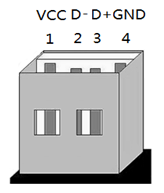
USB communication refers to communication between controllers and devices. The computer host is the controller, and Telink USB is the device. The host referenced later is the default controller. A USB bus is a unidirectional bus; communication can only be initiated by the controller. When the device receives a request from the controller, it sends data to the controller. The controller sends requests to the device every n units, where n is the user's configuration parameter.
USB has four operating speeds: ultra-high speed (5.0 Gbit/s), high speed (480 Mbit/s), full-speed (12 Mbit/s), and low speed (1.5 Mbit/s). The communication frame cycle for full-speed and low-speed USB buses (the interval between sending data between two consecutive frames) is 1ms, while for high-speed USB buses is 125 microseconds. USB 1.1 only supports full speed and low speed, USB 2.0 supports high speed, full speed, and low speed, and ultra speed is only supported in USB 3.0.
USB packet format and transfer process
A packet is the most basic unit of USB data transmission, meaning each data transfer is carried out in the form of a packet. A packet must be composed of transactions to enable effective communication. Depending on communication needs, there are various packets used to organize different transactions (IN, OUT, SETUP). One or more transactions form a single transmission (control transmission, batch transmission, terminal transmission, and isotime transmission).
A packet is the smallest unit of data transmitted on a USB bus and cannot be interrupted or interfered with, otherwise errors occur. Several packets form a single transaction, and even a single transaction cannot be interrupted, meaning it is a few packets belonging to a single transaction.
(1) USB package structure
A packet is the basic unit for information transmission in USB systems; all data is packaged and transmitted over the bus.
As shown in the figure below, a USB packet consists of seven parts: Sync Domain (SYNC), Packet Identifier (PID), Address Domain (ADDR), Endpoint Domain (ENDP), Frame Number Domain (FRAM), Data Domain (DATA), and Validation Domain (CRC). Note that not every USB packet contains all seven domains mentioned above; in other words, some packages only contain a few of them.
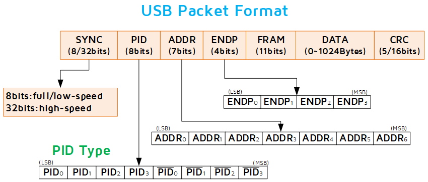
1) Synchronous domain
The synchronization domain mainly notifies the other party of the start of data transmission and provides a synchronization clock. For low-speed and full-speed devices, the synchronous domain uses 0000 0001 (binary number); For high-speed equipment, the 00000001 used is 000000000000000000000.
2) Packet Identifier (PID)
Packet identifier is mainly used to identify the type of packet and consists of 8 bits: the lower 4 bits are PID codes, the upper 4 bits are the validation fields, which are inverted from the lower 4 bits. In USB, various packets are distinguished by PID fields.
3) Address field
Since there may be multiple devices connected to the USB bus, an address domain needs to be introduced to distinguish which device is currently communicating. The address field contains 7 data bits, with up to 128 addresses specified. Address 0 is used as the default address and is not assigned to USB devices. For each device on the USB bus, the address is unique.
4) Endpoint field
The endpoint field specifies an endpoint number for a device on the USB bus, containing 4 data bits; Full-speed/high-speed devices can contain up to 16 endpoints, while low-speed devices can have up to 3 endpoints. All USB devices must contain a terminal with a terminal number 0 for exchanging basic information between the host and the device. Except for endpoint 0, all other endpoints are specific to specific USB devices. The combination of address and endpoint domains clarifies the communication channel between the host and the device.
5) Frame number field
The frame number field indicates the frame number of the current frame. It is only sent in the SOF token packet at the start of each frame/microframe, with a data bit length of 11 bits. For each transmitted frame, the host increments it by 1, and it resets to zero when it reaches a maximum of 7 FFH.
6) Data field
The data field contains the data to be transferred between the host and USB devices, measured in bytes, with a maximum length of 1024, and the actual length depends on the specific transmission situation.
7) Checksum field
The checksum field is mainly used to verify the correctness of communication data. CRC is used in both USB token packages and data packets. However, CRC is generated by the sender before bit filling, so the receiver must decode the CRC field after removing bit filling. The PID field in the packet itself contains a checksum, so CRC calculations do not include the PID part. The CRC of the token package uses 5 bits, while the data fields in the packet use 16 bits of CRC.
a. Token pack
SOF packets are sent by the host to the device: for full-speed buses, they are sent every 1.00 ms ±0.0005 ms; For the high-speed bus, it is sent every 125μs ±0.0625μs.
SOF packet format
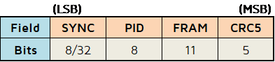
IN, OUT, SETUP packet format

b. Data packets
Data packets (DATA0, DATA1, DATA2, MDATA)
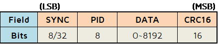
c. Handshake packet
PRE, ACK, NAK, STALL, NYET packet formats
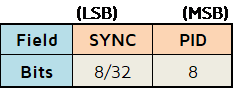
(2) USB transfer process
1) USB transactions
The process of receiving or sending data on a USB is called transaction processing. Transactions usually consist of a series of packets, and different transactions have different packets. Common transactions in USB data transfer include input (IN) transactions, output (OUT) transactions, and SETUP transactions. Note that SOF only indicates the start of a frame; there is no valid data and it is not a transaction; A level state after the EOF frame transmission ends, and it is not a transaction.
A transaction usually consists of two or three packets: a token packet, a data packet, and a handshake packet. The token packet initiates the transaction, the data packet transmits data, and the sender of the handshake packet is usually the data receiver. After the data is correctly received, the handshake packet is sent. The device can also use NACK to indicate that the data is not ready.
2) Input transactions
An input (IN) transaction is the process by which the host retrieves data from an endpoint of a USB device. As shown in the figure below, an input transaction has three states: a normal input transaction (Figure (a)), an input transaction when the device is busy or without data (Figure (b)), and an input transaction when the device fails (Figure (c)). A correct input transaction consists of three stages: token packet, data packet, and handshake packet.
Enter the transaction processing flow



Combining a normal input transaction instance, this chapter introduces and analyzes a normal input transaction. As shown in the figure below, a normal input transaction consists of three interaction processes: (1) The Host sends an IN token packet to the Device; (2) After receiving the IN token packet, the Device sends the data to be sent to the host; (3) After the host receives the data packet, it returns an ACK packet to confirm that the packet was received correctly.
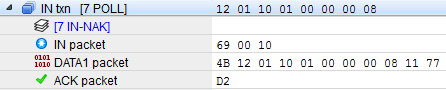
3) Output transactions
An output (OUT) transaction is the process by which the host sends data to a certain endpoint of a USB device. As shown in the figure below, an output transaction has three states: a normal output transaction (Figure (a)), an output transaction when the device is busy (Figure (b)), and an output transaction when the device fails (Figure (c)). A proper output transaction includes three stages: token, data, and handshake.
Output transaction processing flow



Below, using examples of normal output transactions, this chapter introduce and analyze normal output transactions. As shown in the figure below, a normal output transaction involves three interaction processes: (1) The Host sends an OUT token packet to the Device; (2) The Host sends data packets to the Device; (3) After receiving the data packet, the Device replies with an ACK packet to confirm that the packet was received correctly.
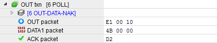
4) Setup transactions
SETUP transaction processing defines special data transfers between Host and Device, which are only applicable during the establishment phase of USB controlled transfers. As shown in the figure below, there are usually three states for setting up transactions: normal transaction setup (Figure (a)), busy device configuration transaction (Figure (b)), and device error transaction setup (Figure (c)). Proper transaction setup includes three stages: token, data, and handshake.
Setup transaction processing workflows



Below, we introduce and analyze normal setup transactions in conjunction with examples of normal setup transactions. As shown in the figure below, a normal setup transaction involves three interaction processes: (1) The host sends a SETUP token packet to the Device; (2) The Host sends a DATA0 packet to the Device; (3) After receiving the data packet, the Device replies with an ACK packet to confirm that the packet was received correctly.

(3) USB transfer
Transfers consist of transactions such as OUT, IN, or SETUP. The USB standard protocol defines four types of transfers: Control Transfer, Bulk Transfer, Interrupt Transfer, and Isochronous Transfer. The priority of the four transfer types from highest to lowest is: synchronous transfer, interrupt transfer, control transfer, and batch transfer.
1) Control transfer
Control Transfer is the most basic and important transmission method in USB and is the default transmission method for port 0. Control transfer is typically used for transferring between the host and the USB peripheral at the endpoint 0, but the specified vendor's control transmission may be used on other endpoints, mainly for querying, configuring, and sending general commands to USB devices. Control transfer is unidirectional (except for endpoint 0, which is bidirectional), and the data volume is usually small. The maximum length of Control Transfer's data packets depends on their operating speed: the maximum packet length for low-speed mode is fixed at 8 bytes, for high-speed mode is 64 bytes, and for full-speed mode, you can choose between 8, 16, 32, or 64 bytes.
Note
- Telink USB endpoint 0 packet length: TC platform (B80/B80B/B85/B87/TC121x) is fixed at 8 bytes; B91/B92/TL321x/TL721x/TL751x can be configured to 8/16/32/64 bytes via
usbhw_set_ctrl_ep_size(). - Control transfer consists of three stages: the setup stage, the data stage (optional), and the state stage, each consisting of one or multiple (data phase) transactions.
- Setup stage: As shown in the figure, the setup stage consists of SETUP transactions. The data stage of a SETLUP transaction is always DATA0 and has a fixed length of 8 bytes.
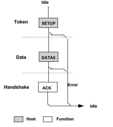
Data Stage: Data Stage is optional. If there is a data stage, it includes one or more IN/OUT transactions. Used to transmit data required during the setup stage, with USB definition format. Transactions in the data stage follow the same direction, meaning either all are in or all are OUT. If the data to be transmitted exceeds the length of a packet, the master controller splits it into multiple packets for transmission. Once the direction of data transmission changes, it is considered to have entered a state process. The first packet of the data process must be DATA1, and after each attempt to transmit one packet, it is exchanged between DATA0 and DATA1. If the last packet size equals the maximum size, another packet of size 0 should be passed to confirm the end. According to the direction of data transmission during the data stage, control transfer can be divided into three types: Control Write, Control Read, and No-Data Control, as shown in the figure below
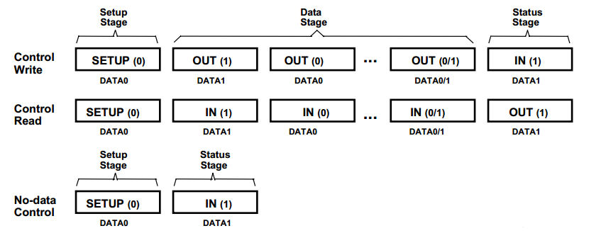
State Stage: The state stage is the final stage of controlling transaction processing, consisting of an IN or OUT transaction, always using DATA1 packets. The state stage and the data stage are transmitted in opposite directions; that is, if the data stage is IN, the state phase is OUT, and vice versa. Used to report the transmission results during the setup and data stages.
2) Interrupt transfer
Interrupt Transfer is the same process as batch transmission except that it does not support PING and NYET packets, so its sequence diagram can be referenced for batch transfer. The main differences between interrupt transfer and batch transfer are two main points: (1) The priority is different—interrupt transfer has a higher priority than batch transfer and is second only to synchronous transmission; (2) Different maximum package lengths are supported: the maximum packet length for interrupt transfer is 8 bytes in low-speed mode, 64 bytes in full-speed mode, and 1024 bytes in high-speed mode.
It should be noted that the interrupt mentioned here is different from hardware interrupts. Since USB does not support hardware interrupts, the host must periodically poll to find out if any devices need to transmit data to the host. From this, it can be seen that interrupt transfer is also a polling process. The polling cycle is determined by the user's device (the polling interval for full-speed equipment is 1ms\~255ms, for low-speed devices 10ms\~255ms). The host only needs to ensure that the transmission is scheduled once within this interval. Polling cycles are very important. If they are too fast, they consume too much bus bandwidth; if too low, data may be lost. Therefore, users need to set them according to their own data conditions.
Interrupt transfer is usually used in devices with limited data volumes but strict time requirements, such as keyboards and mice in human-machine interface devices (HID). Interrupt transfer can also be used to continuously monitor device status, and when conditions are met, batch transfer is used to transfer large amounts of data. The type of endpoint for interrupt transfer is generally the IN endpoint, i.e., from Device to Host (IN transaction), and is rarely used for OUT endpoints. Some computers do not even support OUT transactions for interrupt transfer.
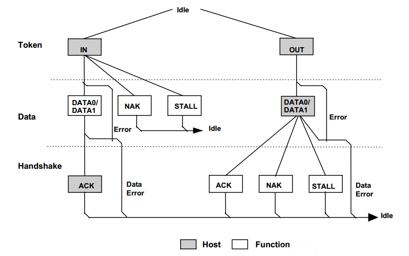
3) Isochronous transfer
Isochronous Transfer, also known as isochronous transmission, is unreliable transmission. Isochronous transfer only has two stages: token packets (IN/OUT token packets) and data packets (DATAx). It does not have handshake packets nor supports PID flipping. When scheduling transfers, synchronous transfer has the highest priority. The maximum length of isochronous transfer packets is 1023 bytes in full-speed mode, 1024 bytes in high-speed mode, and does not support synchronous transmission in low-speed mode.
Isochronous transfer is suitable for data that must arrive at a fixed rate or at a specified time, and can tolerate occasional errors. USB reserves bus bandwidth for it, ensuring service is received within every frame or small frame. Accurate rates and predictable transmission times. However, it does not use error control or retransmission mechanisms, so every transmission is not guaranteed. It is suitable for audio and video devices.
4) Batch transfer
Bulk Transfer, also known as block transfer, is a one-way reliable transmission consisting of one or more IN/OUT transactions, with data packets in each transaction arranged as DATA0-DATA1-DATA0-... to ensure synchronization between the transmitter and receiver, as shown in the figure below.
Error detection and retransmission mechanisms in USB are handled by hardware. If a transfer error occurs, the DATA packet will not be flipped and will be resent. At the same time, if the receiver receives a DATA packet with the same consecutive PID, it is treated as a retransmission packet. USB allows up to 3 consecutive transmission errors; if more than 3 occur, the host considers the endpoint to have a functional error (STALL) and abandons the transmission task for that endpoint.
USB applications — basic concept
The USB applications discussed in this chapter do not refer to the purpose of USB, but rather to the application layer design above the USB driver layer. This chapter explains the basic concepts and working principles of USB in detail from the user's perspective, helping users become familiar with and master the basics and usage of USB.
The relationship between USB hardware devices and software devices is that a single USB hardware device can correspond to one or more software devices, depending on the user's enumerated information (configuration descriptor information). Software devices are virtual devices that the PC abstracts from the interfaces of hardware devices that implement the same function, allowing unified operation. A software device contains one or more interfaces, and an interface contains one or more endpoints (endpoints are explained below), and interfaces and endpoints are all concepts in hardware devices.
An endpoint is the smallest unit in a USB device capable of transmitting and receiving data. Except for endpoint 0 (fixed for bidirectional control transmission), all other endpoints only support unidirectional communication, i.e., the input endpoint (data stream from device to host) or output endpoint (data stream from host to device). There is a limit to the number of endpoints supported by devices. Besides the default endpoint 0, low-speed devices can support up to 2 sets of endpoints (2 inputs, 2 outputs), while high-speed and full-speed devices can support up to 15 sets of endpoints.
An interface is a collection of endpoints that form a basic function within a USB device, and is controlled by the USB device driver (the host can, based on the interface, virtually operate a USB device on the PC side, which is a class of USB devices). From the host's perspective, a USB device can consist of one or more interfaces. For example, a USB device integrating a mouse and keyboard has two interfaces: one keyboard and the other mouse; For example, an audio device consists of an interface for command transmission and an interface for data transmission.
Summary as follows:
Endpoint: The endpoint is the only identifiable part of a USB device. It is the endpoint of communication flow between the host and the device. It serves as a data buffer on the USB device or host, used to store and transmit various USB data.
Interface: can be understood as a function.
Configuration: The combination of interfaces, selected during connection.
Standard descriptors
A descriptor is a set of data used to describe device attributes, divided into standard descriptors and proprietary descriptors. Standard descriptors are common attribute descriptions for all USB device types, including device descriptors, configuration descriptors, interface descriptors, endpoint descriptors, and string descriptors. Among them, string descriptors are further divided into serial number descriptors, product descriptors, vendor descriptors, and language ID descriptors. Proprietary descriptors are descriptors unique to each device class. For example, HID descriptors include HID descriptors, report descriptors, and entity descriptors. The diagram below shows the standard device request structure specified by the USB protocol.
(1) Device descriptors
Device descriptors describe basic information about USB devices, and each device has only one device descriptor. The diagram below shows the structure of a standard device descriptor. The first 8 bytes summarize the basic attributes of USB, which is the first information the host needs to obtain in USB enumeration.
| Offset | Domain | Size | Value | Description |
|---|---|---|---|---|
| 0 | bLength | 1 | Numbers | The byte count of this descriptive table |
| 1 | bDescriptorType | 1 | Constant | Descriptor type (here it should be 0x01, i.e., device descriptor) |
| 2 | bcdUSB | 2 | BCD code | USB device specification version number (BCD code) for this device compatible with the description table |
| 4 | bDeviceClass | 1 | Class | Device classification code |
| 5 | bDeviceSubClass | 1 | Subclass | Subclass masking |
| 6 | bDeviceProtocol | 1 | Protocol | Protocol code |
| 7 | bMaxPacketSize0 | 1 | Numbers | Maximum packet size at endpoint 0 (only 8, 16, 32, 64 are valid values) |
| 8 | idVendor | 2 | ID | Manufacturer Logo (assigned by USB-IF organization) |
| 10 | idProduct | 2 | ID | Product Logo (assigned by manufacturer) |
| 12 | bcdDevice | 2 | BCD code | Device Serial Number (BCD Code) |
| 14 | iManufacturer | 1 | Index | The index value of a string descriptor describing vendor information. |
| 15 | iProduct | 1 | Index | The index value of the string descriptor describing product information. |
| 16 | iSerialNumber | 1 | Index | The index value of the string descriptor describing the device serial number information. |
| 17 | bNumConfigurations | 1 | Numbers | Possible number of configuration descriptors |
Note
- idVendor(VID) and idProduct (PID) are used to uniquely identify a device, but for Windows, simply giving VID and PID does not uniquely identify the device, resulting in continuous driver installations. At this point, you also need to consider the serial number string. That is, when only VID, PID, and serial numbers match, Windows only needs to install the driver once.
- The index values of the three string descriptors should be different (except 0).
(2) Configuration descriptors
Configuration descriptors define the configuration information of a device, and a device can have multiple configuration descriptors.
| Offset | Domain | Size | Value | Description |
|---|---|---|---|---|
| 0 | bLength | 1 | Number | This describes the byte length of the table. |
| 1 | bDescriptorType | 1 | Constant | Configure the description table type (here it is 0x02) |
| 2 | wTotalLength | 2 | Number | The total length of this configuration information (including configuration, interfaces, and endpoint descriptors) |
| 4 | bNumInterfaces | 1 | Number | Number of interfaces supported by this configuration |
| 5 | bConfigurationValue | 1 | Number | Use this configuration |
| 6 | iConfiguration | 1 | Index | The string description table describing this configuration index (0-none) |
| 7 | bmAttributes | 1 | Bitmap | Configuration Features: D7: Reserve (set to 1) D6: Self-contained power D5: Remote wake-up D4: 0: Keep (set to one) |
| 8 | MaxPower | 1 | mA | In this configuration, the bus power consumption is measured in units of 2mA |
(3) Interface descriptors
Interface descriptors describe the configuration provided by an interface, and the number of interfaces a configuration has is determined by the bNumInterfaces of the configuration descriptor.
| Offset | Domain | Size | Value | Description |
|---|---|---|---|---|
| 0 | bLength | 1 | Number | The number of bytes in this table is |
| 1 | bDescriptorType | 1 | Constant | Interface Description Table Class (here should be 0x04) |
| 2 | bInterfaceNumber | 1 | Number | Interface number, the index of the currently configured supported interface array (starting from zero). |
| 3 | bAlternateSetting | 1 | Number | Optional index values. |
| 4 | bNumEndpoints | 1 | Number | The number of endpoints used for this interface is except for endpoint 0 |
| 5 | bInterfaceClass | 1 | Class | The class value of the interface is |
| 6 | bInterfaceSubClass | 1 | Subclass | Subclass code |
| 7 | bInterfaceProtocol | 1 | Protocol | Protocol code: depends on the values of the bInterfaceClass and bInterface SubClass fields. |
| 8 | iInterface | 1 | Index | The string describing this interface describes the index value of the table. |
(4) Endpoint descriptors
Each endpoint in a USB device has its own endpoint descriptor, and the number of these is determined by the bNumEndpoint in the interface descriptor.
| Offset | Domain | Size | Value | Description |
|---|---|---|---|---|
| 0 | bLength | 1 | Number | The byte length of this descriptive table is |
| 1 | bDescriptorType | 1 | Constant | Endpoint description table class (here should be 0x05) |
| 2 | bEndpointAddress | 1 | Endpoint | The endpoint address and direction described in this table: Bit 3..0: Endpoint number. Endpoint numbers cannot be duplicated during configuration changes; Bit 6:4: Retention, zero; Bit 7: Direction, omitted if controlling endpoints. 0: Output Endpoint (Host to Device) 1: Input Endpoint (Device to Host) |
| 3 | bmAttributes | 1 | Bitmap | Characteristics of the endpoint. Bit 1..0: Transfer type 00=Control transmission 01=Synchronous transmission 10=Batch transfer 11=Interrupt transmission |
| 4 | wMaxPacketSize | 2 | Number | The maximum size of data packets this endpoint can receive or send under the current configuration. For interrupt transfer, batch transfer, and control transfer, endpoints may send shorter packets. |
| 6 | bInterval | 1 | Number | The host polls the interval of this endpoint and ignores endpoints for batch and control transmissions; For synchronous transmission endpoints, it must be 1; For interrupted transmission, the low-speed mode is 10\~255 (ms) here, and the full-speed mode is 1\~255 (ms). |
(5) String descriptors
String descriptors are optional. If string descriptors are not supported, all indices of string descriptors in the device, configuration, and interface descriptors must be set to 0, and the language string descriptor index must be 0.
| Offset | Domain | Size | Value | Description |
|---|---|---|---|---|
| 0 | bLength | 1 | Number | The number of bytes in this describing table (the value of the bString field N+2) |
| 1 | bDescriptorType | 1 | Constant | String description table type (here should be 0x03) |
| 2 | bString | N | Number | UNICODE-encoded string |
USB enumeration
Enumeration means the host reads some information from the device side, knows what kind of device it is, and how it communicates, so the host can load the appropriate driver based on this information. A crucial part of debugging USB devices is to check the USB enumeration. As long as the enumeration succeeds, it is close to the success.. Below, we provide a detailed introduction to the USB enumeration process using a USB enumeration diagram (see diagram (a) below) and a Telink mouse-type USB enumeration example (see diagram (b)).
(1) USB enumeration sequence
Figure (a) below shows the USB enumeration sequence diagram. From the diagram, we can see that the USB enumeration process is completed in 8 steps, with steps 1~7 being standard USB enumeration steps, and Step 8 being the USB device-specific enumeration process.
- Step 1 After the host detects a device is connected: First, the host determines whether the device is low-speed or full-speed based on the level status on the differential signal line (high-speed devices default to full-speed equipment at the initial power-on); Then the host waits for the device power to stabilize (>=100ms), and sends a reset signal to the device (D+ and D- are both low, sustaining >=10ms); Finally, if the device is high-speed and the host (hub) supports high-speed mode, after high-speed detection and handshake between the host and device, the device can switch to high-speed mode; otherwise, it will remain in full-speed mode.
- Step 2: After completing Step 1, the host uses endpoint 0 (default endpoint, controlling transmission) to send a GetDescriptor request (device address is 0). After receiving the request, the device sends its device descriptor to the host, which then proceeds to the next step based on this device descriptor (bMaxPacketSize0 field). It should be noted: (1) Only when the device receives the reset signal in Step 1 will it respond to the host; (2) The device that has completed the enumeration does not respond to the request; (3) The descriptor must be at least 8 bytes long (the bMaxPacketSize0 field is at the 8th byte); (4) If the device times out and does not respond or responds incorrectly, the host will restart and try three times. If after three attempts still does not receive a correct response, the host considers the device to be unrecognized (same below).
- Step 3: After correctly completing Step 2 and obtaining the maximum packet length at endpoint 0, the host resets the device, then depackaged and bundled the packets according to this length.
- Step 4: The host assigns a non-zero address to the device, which is different from other devices on the hub and is used to ensure the stability of directional communication. After the host completes the address device, communication between the host and the device will continue to follow the new address until the device is reset or removed.
- Step 5: The host sequentially obtains the device's standard descriptor (device descriptor, configuration descriptor, interface descriptor, endpoint descriptor, and string descriptor) according to the new address in Step 4. Note: (1) The length of the device descriptor is already obtained by the host in Step 2, so the length specified by the host (maximum length is the device descriptor length) is used to get the device descriptor. Other descriptors are obtained according to the maximum length of 255. The device side only needs to send the actual length as needed; (2) Device interface descriptors, endpoint descriptors, etc., which may be included in the configuration descriptor. The host retrieves all data for that configuration based on the wTotalLength field in the configuration descriptor; (3) If the device has multiple configurations, the host will request configuration descriptors in multiple instances; (4) The host will request string descriptors in order according to the number of string descriptors contained in device, configuration, interface, and endpoint, according to their index values. A special string descriptor (speech information descriptor) with an index value of 0 is used.
- Step 6: After completing Step 5, the host obtains the actual length of the configuration descriptor, sequentially obtaining the descriptor information and other information contained in the descriptor (such as interface descriptor and endpoint descriptor, etc.).
- Step 7 Step 1 \~6 is the standard USB enumeration process. Only when steps 1 \~6 are correct will the host issue a SetConfiguration command to activate and use a configuration on the device, at which point the device is truly usable. After the device configuration is complete, the host divides the device into one or more virtual devices based on the standard device descriptors.
- Step 8 After Step 7 is completed, one or more virtual devices are generated on the host, each with its own category identifier. The host will query the corresponding driver based on its VID, PID, and serial number, and install the driver (if there is a backup on the host, use it directly and do not install it again). Then, the host loads the class-specific description information according to the driver. Here is the standard HID device, with the main unit having its own driver.
(2) USB enumeration examples
Figure (b) below shows the enumeration process for the Telink Dongle mouse device. Step x in the diagram corresponds one-to-one with Step x in Figure (a). Step 8 is the proprietary enumeration process for the HID device class, which retrieves the report descriptor. The structure of the report descriptor can refer to the USB HID protocol Universal Serial Bus (USB) - Device Class Definition for Human Interface Devices (HID)。
Overview of USB types
Telink chips are divided into two types of USB hardware modules based on supported USB versions and speed modes:
- Full-speed USB (FS): Only full-speed mode (12Mbps). Uses a fixed-direction endpoint design and 8+256 Bytes of dedicated RAM.
- High-Speed USB (HS): Supports USB 2.0 protocol, as well as high-speed mode (480Mbps) and full-speed mode (12Mbps). It features a bidirectional endpoint design, built-in DMA engine, and 8KB FIFO.
Full Speed USB (FS)
Full Speed USB is the 12Mbps USB mode used by most Telink chips.
Supported chips can be found in the Chip USB version overview.
Main features:
- Fixed directional endpoints (IN/OUT directions cannot be switched)
- TC platform (B80/B80B/B85/B87/TC121x) endpoint 0 fixed at 8 bytes
- TL platform (B91/B92/TL321x/TL721x/TL751x) endpoint 0 can be configured with 8/16/32/64 bytes
- Supports both manual and automatic modes
For details, see Full Speed USB (FS).
High-speed USB (HS)
High-Speed USB supports 480Mbps high-speed mode and is backward compatible with full-speed 12Mbps mode.
Main features:
- USB 2.0 protocol, supporting both High Speed and Full Speed
- Device-Only operating mode
- There are 9 bidirectional endpoints (EP0-EP8), with EP0 being dedicated control endpoints
- 8KB internal FIFO, built-in DMA (Descriptor DMA)
- UTMI+ PHY interface
- Supports four types of transfer: Control, Bulk, Interrupt, and Isochronous
For details, see High-Speed USB (HS).
Overview of the USB version of the chip
| Chips | Speed mode | Number of endpoints (EP0+EP1-EP8) | SRAM size (EP0+EP1-EP8 endpoints shared) |
|---|---|---|---|
| B80/B80B/B85/B87/TC121x/B91 | Full speed | 1+8 | 8+256 Bytes |
| B92 | Full speed | 1+8 | 8+1024 Bytes |
| TL321x/TL721x/TL751x | Full speed | 1+8 | 64+2048 Bytes |
| TL322x | Full-speed + high-speed | 1+8 | 64 +8192 Bytes |
Note
- TC321x/TL323x/TC122x do not support USB hardware modules and cannot use USB functionality.
Full Speed USB (FS)
Introduction to USB hardware
Telink USB hardware modules internally solidify the processing of raw packets and transactions, automatically saving IN endpoint data and sending OUT endpoint data, packaging endpoint 0 data into standard user data packets. This not only improves USB execution efficiency but also greatly reduces the complexity of USB development.
(1) SRAM 8+256
Endpoint 0 can both input and output; the other endpoints have the following directions:
| Configurable endpoint types | Endpoint number |
|---|---|
| Control Endpoint (Input/Output) | 0 |
| Output endpoint | 5, 6 |
| Input endpoint | 1, 2, 3, 4, 7, and 8 |
Memory: 8+256 bytes of dedicated USB RAM. Endpoint 0 is fixed at 8 bytes, while the other endpoints share 256 bytes. The endpoint cache size is the starting address of the next endpoint minus the starting address of this endpoint.
| Endpoint start address | Meaning |
|---|---|
| 0x00 | Endpoint 1 starting address |
| 0x08 | Endpoint 2 starting address |
| 0x10 | Endpoint 3 starting address |
| 0x20 | Endpoint 6 starting address |
| 0xc0 | Endpoint 5 starting address |
Note
- The maximum endpoint cache is determined by the max register (which can be allocated to all cache space), with a default of 64 bytes.
- Compatible chipsets: B80/B80B/B85/B87/TC121x/B91 (SRAM: 8+256 Bytes)
(2) SRAM 8+1024
The endpoint orientation is consistent with 3.1.1. The following features have been added to version 3.1.1:
- Endpoint addresses are set via
usbhw_set_ep_addr(),supporting 16-bit addresses (up to 8-bit addresses supported viareg_usb_ep_buf_addrh) - Endpoint pointers support 16 bits (obtained via
usbhw_get_ep_ptr(),reg_usb_ep_ptrhsupports up to 8 bits)
Compatible chip: B92 (SRAM: endpoint 0 fixed 8 bytes + shared 1024 bytes).
(3) SRAM 64+2048
The endpoint orientation is consistent with 3.1.1. Based on version 3.1.2, the following has been added:
Endpoint 0 Packet size configurable (set to 8/16/32/64 bytes via usbhw_set_ctrl_ep_size())
Compatible chips: TL321x/TL721x/TL751x (SRAM: Endpoint 0 64 bytes + shared 2048 bytes).
Interrupt
USB interrupts can be divided into three categories: endpoint 0 interrupts, endpoint 1-8 interrupts, and suspend/250us/reset interrupts, as shown in the table below:
| Interrupt | Conditions for generation | Clearing methods |
|---|---|---|
| CTRL_EP_SETUP(IRQ7) | Endpoint 0 controls the transmission setup stage | Manually clear status |
| CTRL_EP_DATA (IRQ8) | Endpoint 0 controls the data transfer stage | Manually clear status |
| CTRL_EP_STATUS (IRQ9) | Endpoint 0 controls the transmission state stage | Manually clear status |
| Endpoint(1-8) interrupts(IRQ11)FLD_USB_EDP8_IRQ (in)FLD_USB_EDP1_IRQ (in)FLD_USB_EDP2_IRQ (in)FLD_USB_EDP3_IRQ (in)FLD_USB_EDP4_IRQ (in)FLD_USB_EDP5_IRQ (out)FLD_USB_EDP6_IRQ (out)FLD_USB_EDP7_IRQ (in) | 1. Except for synchronous endpoints: output endpoint: host out transaction, corresponding position of the status register. 1. An interrupt occurs, and after reception, it returns to ACK. Input endpoint: After data filling is complete, configure the ACK to notify the hardware and trigger an interrupt. The hardware, upon receiving the host-in transaction, sends data to the host. 2. Synchronization endpoints: Endpoints 6 and 7 can be set as synchronization endpoints, with interrupts occurring at intervals of 1 ms. | Manually clear status |
| USB_IRQ_USB_SUSPEND (IRQ24) | The USB bus is idle, for example, if the USB port is unplugged, the host goes to sleep | Manually clear status |
| USB_IRQ_250us (IRQ34) | 250us scheduled interrupts | Manually clear status |
| USB_IRQ_RESET (IRQ35) | Host sends reset timing | Manually clear status |
Note
- The transmission of the Driver enumeration process is handled by polling without interrupts.
Automatic and manual modes
Telink USB offers two modes: automatic mode and manual mode:
Users can control whether to choose automatic or manual mode by configuring the configuration register at endpoint 0. The default configuration register for endpoint 0 is 0xFF, i.e., automatic mode. At this time, all codecs related to USB endpoint 0 are automatically driven by Telink hardware. Telink has its own driver as a Print device, using endpoint 8 as the control interface endpoint, and printer data is sent from endpoint 0;
Manual mode requires users to modify EDP0CFG registers (see below), usually setting bit[7] and bit[5] to 0, meaning the user performs the standard USB enumeration and uses user-defined descriptors.
USB software basics
(1) USB operation process
The Telink USB software operation process can be divided into two stages: initialization and loop detection, as shown in the diagram below.
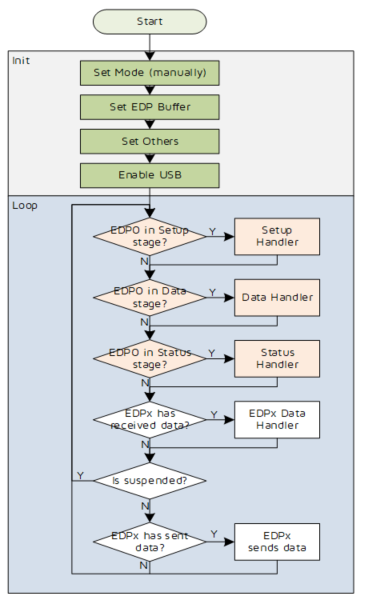
The initialization stage mainly completes USB configuration and enabling USB. USB configuration options mainly include mode switching (automatic and manual), setting USB data buffers, and configuring other configuration items; Mode switching mainly switches the USB operating mode to manual mode. At this time, the enumeration process and descriptors are controlled by the user, and the device reports the user's prepared enumeration information to the host; Setting a USB buffer allows users to specify a buffer segment for each endpoint based on their usage (except for endpoint 0). The buffer total size is 256 bytes; unused endpoints do not need to be specified; Setting Other Configurations is used to perform other configuration operations. If users do not wish to use the system's default configuration items, they can choose to configure them themselves, such as transmitting data in the form of interrupts.
Loop detection mainly involves continuously checking whether there is data in the data reception and sending buffers. If there is data, it performs related operations. During program execution, it repeatedly executes USB_handle_irq. The operation process of endpoint 0 can be divided into three stages, as shown in the figure below, corresponding to the SETUP stage, DATA stage, and STATUS stage for controlling transmission. These mainly complete USB recognition and configuration operations, such as USB enumeration. This process is completed in the main loop, where SETUP parses commands issued by the host and prepares the corresponding data according to the host's commands; DATA refers to the data prepared during the data phase to be sent to or received by the host; STATUS is the process of both parties shaking hands.
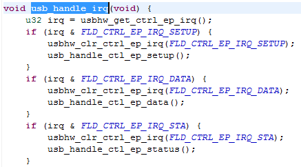
(2) Data reception and transmission
A. Data reception
Telink USB data reception is completed by hardware, which saves the received data to RAM. After reception is complete, the hardware generates an interrupt to notify the user, and the user only needs to read the data after detecting the interrupt. Data detection and reception should be performed within the USB/_handle_irq functions in USB.C. Based on the diagram below, we analyze the processing flow of Telink USB data reception in detail:
1) The user needs to check whether the relevant interrupt identifier bit (reg_usb_irq) is set to 1; if set to 1, the data reception stage begins.
2) Once data is detected, the user needs to clear the interrupt identifier bit, i.e., reg_usb_irq = BIT((USB_EDP_CUSTUM_OUT & 0x07)).
3) Before reading data, users need to use reg_usb_ep_ptr (USB_EDP_CUSTUM_OUT) to obtain the received data length.
4) After obtaining the data length, users can repeatedly read the USBHW_read_ep_data (USB_EDP_CUSTUM_OUT) to obtain all the data received this time.
5) After receiving the data, the user needs to call usbhw_data_ep_ack(USB_EDP_CUSTUM_OUT). (Note: This step is very important. Only when the ACK of the OUT endpoint is set will the hardware receive data sent by the host to that endpoint, and an interrupt will occur after reception is complete.) )
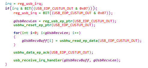
B. Data transmission
Telink USB data sending and receiving are handled by hardware; users only need to fill the data into the corresponding USB RAM and set the data ACK to position 1. Before filling up data, users need to first check whether there is data to be sent in the USB RAM. If there is, they should wait until sending is complete before filling new data; otherwise, data overwriting will occur.
The diagram below shows an example of sending data in the Telink SDK. Below, we analyze the USB data sending process in detail using this example:
1) Before sending data, users need to check whether the operation endpoint is busy. If it is, it must wait for the sending to complete before filling the data.
2) If the endpoint is idle, the endpoint counter needs to be reset first, i.e., reg_usb_ep_ptr(USB_EDP_CUSTUM_CMISC_IN) = 0.
3) After resetting the endpoint counter, users can fill the endpoint with data. Note that reg_usb_ep_dat(USB_EDP_CUSTUM _CMISC_IN) = data[i] is putting data into USB RAM (hardware operation).
4) After the user fills the data, they need to call reg_usb_ep_ctrl(USB_EDP_CUSTUM_CMISC_IN) = FLD_EP_DAT_ACK to notify the hardware that the data is ready. After receiving this command, the hardware will send the data to the host when the next host requests it.
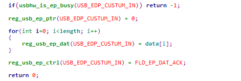
USB Demo
USB applications mainly introduce the simple applications of HID (Human Interface Device) devices, audio devices, and CDC (Communication Device Class) devices within the USB standard device category, which customers can freely combine according to their needs.
HID devices are commonly used types of USB devices, specifically those that interact directly with people, such as USB mouts and USB keyboards;
The most common USB Audio devices are microphones and speakers;
The USB CDC class is the abbreviation for USB communication devices, while virtual serial devices are a type of CDC device.
(1) Demo configuration
In the header file app_config.h, you can choose to configure different devices.
TC Platform (B80/B80B/B85/B87/TC121x):
#define  USB_MOUSE           1
#define  USB_KEYBOARD        2
#define  USB_CDC             3
#if (!MCU_CORE_B80 && !MCU_CORE_B80B)
#define  USB_MICROPHONE      4
#define  USB_SPEAKER         5
#endif
#define  USB_MOUSE_SLEEP     6

#define  USB_DEMO_TYPE       USB_MOUSE
Note
- The B80/B80B do not support USB_MICROPHONE or USB_SPEAKER.
TL Platform (B91/B92/TL321x/TL721x/TL751x):
#define  USB_MOUSE           1
#define  USB_KEYBOARD        2
#define  USB_MICROPHONE      3
#define  USB_SPEAKER         4
#define  USB_CDC             5
#define  USB_MIC_SPEAKER     6

#define  USB_DEMO_TYPE       USB_MOUSE
TL platform demo additionally supports:
USB_MIC_SPEAKER: Microphone and speaker composite deviceUSB_PRINTER_ENABLE: Printer equipmentUSB_SOMATIC_ENABLE: Motion sensing devicesUSB_CUSTOM_HID_REPORT: Custom HID reportsUSB_MASS_STORAGE_ENABLE: Large-capacity storage devices (TL platform only)
(2) USB Mouse
A. Mouse processing workflow
USB HID devices transmit data through reports. A single report descriptor can describe multiple reports, and different reports are identified by their IDs. The report ID is the first byte of the report. If there is no specified report ID, the report has no ID field; it starts with data. For detailed report descriptor information, refer to the USB HID protocol and HID Usage Tables.
First, the host recognizes the Telink USB as a mouse device and needs to go through the enumeration stage. After successful device enumeration, it enters the data transmission and reception stage. According to the content of the mouse report descriptor, the descriptor with report ID USB_HID_MOUSE contains 4 bytes. The lowest 5 bits of the first byte indicate whether the key is pressed; the higher 3 bits are constants and are useless; Byte 2 is the change in the X-axis; The 3rd byte is the change in the Y-axis; Byte 4 is the change in the scroll wheel. Returns the report via the function usbmouse_hid_report(USB_HID_MOUSE, mouse, 4).
In the demo program, the array unsigned char mouse[4] is defined, where:
mouse[0]:BIT(0) - left key; BIT(1) - right key; BIT(2) - middle key; BIT(3) - side key; BIT(4) - external key。 The corresponding bit is set to 1, which means pressing the mouse buttonmouse[1]: The change in relative to the X coordinatemouse[2]: The change in relative to the Y coordinatemouse[3]: The amount of change in the scroll wheel
B. Mouse test
Press Test
In the demo program, report ID:USB_HID_MOUSE = 1,
Array mouse assignment: mouse[0] = BIT(1), mouse[1] = -2 (complement), mouse[2] = 2, mouse[3] = 2.
After grounding the pins on the development board and then pulling them out, function usbmouse_hid_report(USB_HID_MOUSE, mouse, 4) is executed.
You can observe that when the desktop right-click the mouse is pressed, the cursor moves down to the left, as shown below. You can also see in the USB packet capture tool Input Report[1]: x:-2, Y:2, wheel:0, Btns=[2].

Release test
Repeat the same operation on the other pin: the mouse array is reset and the key is released.
(3) USB Keyboard
A. Keyboard processing workflow
According to the content of the keyboard report descriptor, there are input and output reports. The input report specifies 8 bytes, and the 8 bits of the first byte indicate whether a special key is pressed:
- BYTE0:BIT(0) – left Ctl; BIT(1) – Left Shift; BIT(2) – Left Alt; BIT(3) – left GUI; BIT(4) – Right Ctl; BIT(5) – Right Shift; BIT(6) – Right Alt; BIT(7) – Right GUI
- BYTE1: Reserved value, all set to 0
Bytes 3 to 8 are the standard key values; when no key is pressed, all 6 bytes are 0. The first byte value of these 6 bytes is the key value of the key. When multiple keys are pressed simultaneously, all these key values are returned simultaneously. The order of key values in the array is not related. For specific key values, please refer to the HID Purpose Table documentation, for example: 0x59 corresponds to numeric keyboard 1; 0x5a corresponds to numeric keyboard 2; 0x5b corresponds to numeric keypad 3; 0x39 corresponds to case-toggle keys.
B. Keyboard test
Press Test
In the Demo program, define array kb_data[6], assign the value kb_data[0] = 0; kb_data[1] = 0; kb_data[2] = 0x59; kb_data[3] = 0x5a; kb_data[4] = 0x39; kb_data[5] = 0.
After grounding the pins on the development board and then pulling them out, function usbkb_hid_report_normal(0x10, kb_data) will be executed, where parameter 1 corresponds to the first byte and parameter 2 corresponds to an array of 3\~8 bytes.
You can observe that in the input interface of the editing window, you can enter the numbers 1 and 2, and press the right Ctrl key and the capital/case key. As shown in the figure below, you can also see in the USB packet capture tool Input Report: Keys=[Rctrl 1 2 CapsLk].

Release test
Perform the same operation on another pin: the special key and kb_data array are cleared, and the key is released.
(4) USB MIC
A. MIC processing flow
Taking AMIC as an example, a USB microphone device transmits the device's AMIC data to the host via USB, ensuring the sampling rate and number of channels for the entire data channel match. In the demo program, data is mainly uploaded to the USB section. Mic endpoint interrupts are scheduled at 1ms, meaning every 1ms is interrupted. Depending on the sampling rate, the amount of data generated in 1ms varies. For example, for 16K sampling rate audio and mono data, 1 sample equals 2 bytes, 1ms data is 32 bytes, and the corresponding audio buff is filled into the USB SRAM.
TL Platform Differences: TL platform MIC Demo supports dual audio (MIC_CHANNEL_COUNT 2), while TC platform only supports mono (MIC_CHANNEL_COUNT 1).
B. MIC Demo Test
For audio-related testing, using Audacity software, as shown below, select Telink Audio 16 for microphone and PC speakers for speakers.
Device Mic picks up audio and PC speakers play it. If the recorded human voice can be played through the speaker without distortion, it means the Mic is working properly.
 ).
).
(5) USB Speaker
A. Speaker processing workflow
The USB speaker device transmits the host's audio data to the device via USB. This process is completed within 1ms interrupt, reads the length of the USB SRAM data, and fills the corresponding data into the audio buff.
TL platform differences: TL platform Speaker Demo supports dual audio (SPK_CHANNEL_COUNT 2), while TC platform only supports mono (SPK_CHANNEL_COUNT 1).
B. Speaker Demo Test
In the Audacity software, the microphone is PC microphone, and the speaker is Telink Audio 16. Through the output audio interface (3.5mm headphone jack). If the recorded vocals can be played through headphones without distortion, it means the speaker is working properly.
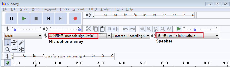
(6) USB CDC
CDC devices have two interfaces: CDC control interface and CDC data interface. The control interface allocates endpoint 2 as the interrupt input endpoint for transmission. The data interface assigns endpoint 5 (out) and endpoint 4 (in). You must first set the ACK of endpoint 5 before the endpoint can receive data from the USB host.
A. CDC processing flow
The first time using a CDC device on a PC, to ensure it is identified as a CDC device, you need to manually install the .inf file, as shown in the diagram below under the USB_Demo path.
Note
- Only Win7 and Win8 systems need to install the .inf file; systems with Win10 and above do not need to install it.
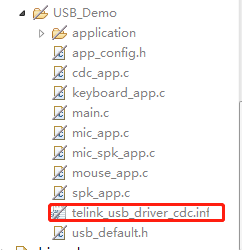
Data Reception (host to device)
In the demo program, the host in the function void usb_cdc_irq_data_process(void) sends data to the device. After endpoint 5 causes an interrupt, function usb_cdc_rx_data_from_host(usb_cdc_data) receives the data.
Data Transmission (Device to Host)
In main_loop, when the received buff data length is not zero, the received data is sent to the host via the function usb_cdc_tx_data_to_host().
TL Platform Differences: The TL platform CDC Demo supports both blocking and non-blocking transmission modes, switching via DEVICE_SEND_DATA_MODE macros. In non-blocking mode, the usb_cdc_tx_data_to_host_non_block() function returns immediately after filling the data. The TL platform CDC Demo requires explicit configuration of endpoint buffer size and address.
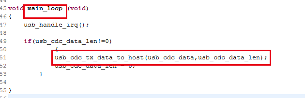
B. CDC Demo Test
The test phenomenon is shown in the figure below, returning data sent by the serial port assistant.
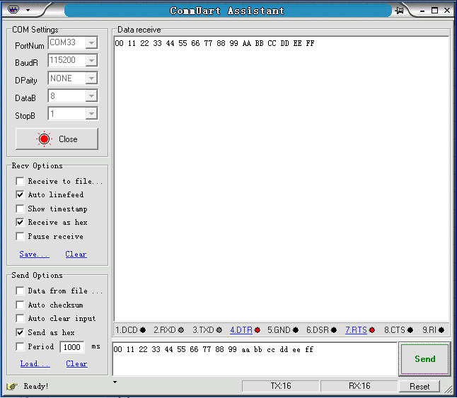
High-speed USB (HS)
High-speed USB hardware architecture
(1) Overview
For an overview of high-speed USB (USB0) types, please refer to High-Speed USB (HS). This chapter provides a detailed introduction to the hardware architecture and driver usage of high-speed USB.
(2) USB0 features
The USB 2.0 Device core used by USB0 has the following features:
| Characteristics | Description |
|---|---|
| USB standard | USB 2.0, supporting both High Speed and Full Speed |
| Working mode | Device-Only |
| Number of endpoints | 9 bidirectional endpoints (EP0\~EP8), with EP0 as a dedicated control endpoint |
| Total size of FIFO | 8KB (8192 bytes) |
| DMA support | Internal DMA (Descriptor DMA) |
| PHY interface | UTMI+ |
| Types of transmission | Control、Bulk、Interrupt、Isochronous |
(3) System block diagram
USB0, as an external device to the CPU, interconnects with the system via the AHB bus, with interrupt signals connected to the interrupt controller:
 +-------------------+          +------------------+          +----------------+
 |                   |  AHB Bus |                  |  UTMI+   |                |
 |      CPU          |<-------->|     USB0         |<-------->|    USB PHY     |
 |                   |          |                  |          |                |
 +-------------------+          +------------------+          +----------------+
         |                              |                           |
         |                              | IRQ_USB0                  | DP/DM
         |                              v                           v
         |                      +-----------------------+        +----------------+
         |                      |                       |        |                |
         +--------------------->|  Interrupt Controller |        |  USB Host      |
                                |                       |        |                |
                                +-----------------------+        +----------------+
IO pins:
| Pins | Function | Description |
|---|---|---|
| PA3 | USB0_DM | USB D - data cable |
| PA4 | USB0_DP | USB D+ data cable |
PA3 and PA4 can only be used as USB0_DM and USB0_DP pins or GPIO functions; they cannot be used simultaneously for other functions.
(4) Endpoints and FIFOs
A. Endpoint type
USB0 supports four types of endpoints defined by the USB 2.0 specification:
| Type | Enumeration value | Description |
|---|---|---|
| Control | USB0_EP_TYPE_CONTROL |
Controlled transmission, supported only by EP0 |
| Isochronous | USB0_EP_TYPE_ISOCHRONOUS |
Isochronous transfer, used for real-time data such as audio/video |
| Bulk | USB0_EP_TYPE_BULK |
Batch transfer, used for large data volumes such as CDC |
| Interrupt | USB0_EP_TYPE_INTERRUPT |
Interrupt transfer, used for periodic transmission of small data volumes such as HID |
B. FIFO architecture
The total internal size of the USB0 FIFO is 8KB, divided into RX FIFO and TX FIFO parts:
- RX FIFO: A single receive FIFO, sharing all OUT endpoints. Set the starting address and size using
usb0hw_set_grxfsiz(). - TX FIFO: Each IN endpoint has its own independent sending FIFO. Configure the start address, size, and FIFO number of each IN endpoint for each IN endpoint via
usb0hw_set_epin_size().
FIFO Address Allocation Example (HID Mouse Demo):
                     +----------------------------+ 0x1FF (8KB)
                     |                            |
                     |   EP2 TX FIFO (64x4 words) |
                     |                            |
                     +----------------------------+ 0x140
                     |                            |
                     |   EP0 TX FIFO (64x4 words) |
                     |                            |
                     +----------------------------+ 0x100
                     |                            |
                     |   RX FIFO (256x4 words)    |
                     |                            |
                     +----------------------------+ 0x000
FIFO size is measured in words. The actual configurable range is limited by the total 8KB FIFO size.
USB0 software architecture
(1) Layered architecture
The USB0 software stack uses a layered architecture design, from top to bottom as follows:
+---------------------------------------------------------------+
| USB Demo layer |
| mouse, keyboard, cdc, audio |
+---------------------------------------------------------------+
| USB Class driver layer |
| (usbd_hid, usbd_cdc, usbd_audio) |
+---------------------------------------------------------------+
| USB Device Protocol Stack |
| (Standard device requests, descriptors, endpoint management) |
+---------------------------------------------------------------+
| Port adaptation layer |
| (usbd_ep_open/write/read/stall + ISR) |
+---------------------------------------------------------------+
| Drive layer |
| (DMA configuration, FIFO management, interrupt handling) |
+---------------------------------------------------------------+
| Hardware layer (USB0 IP) |
| (DMA engine, PHY, endpoint control) |
+---------------------------------------------------------------+
(2) Driver layer
usb0hw.c and usb0hw.h provide the lowest-level operating interfaces of USB0 hardware, including:
- Initialization and Reset:
usb0hw_init(),usb0hw_reset(),usb0hw_power_down(). - Endpoint management:
usb0hw_ep_open(),usb0hw_ep_close(). - Data Transmission:
usb0hw_write_ep_data(),usb0hw_read_ep_data(). - FIFO management:
usb0hw_set_grxfsiz(),usb0hw_set_epin_size(),usb0hw_flush_tx_fifo(), usb0hw_flush_rx_fifo(). - Interrupt management:
usb0hw_get_gintsts(),usb0hw_clear_gintsts(),usb0hw_get_daint(),usb0hw_daintmsk_en(),usb0hw_daintmsk_dis(). - Connection Management:
usb0hw_soft_connect(),usb0hw_soft_disconnect(). - Power management:
usb0hw_pcgc_clk_en(),usb0hw_pcgc_clk_dis(),usb0hw_phy_pll_en(),usb0hw_phy_pll_dis(), usb0hw_remote_wakeup(). - Status query:
usb0hw_get_speed(),usb0hw_get_sof_fn(),usb0hw_get_timer_stamp(). - Other features:
usb0hw_set_address(),usb0hw_test_mode(),usb0hw_set_pwronprgdone().
(3) Port adaptation layer
The port adaptation layer acts as the adaptation layer between USB0 hardware and the USB device protocol stack, achieving the following functions:
- Endpoint Operation Adaptation: Map the protocol stack's
usbd_ep_open(),usbd_ep_write(),usbd_ep_read(),usbd_ep_stall(), usbd_ep_clear_stall() to the` correspondingUSB0HW` functions - SET_ADDRESS Adaptation :
usbd_set_address()callsusb0hw_set_address(). - TEST_MODE Adaptation:
usbd_test_mode()callsusb0hw_test_mode(). - Interrupt Handling:
usb0_irq_handler()handles all USB0 global interrupts registered asIRQ_USB0throughPLIC_ISR_REGISTER
Interrupt handling process (usb0_irq_handler):
usb0_irq_handler()
|
+-- ENUMDONE → Speed check complete, clear the mark
+-- OEPINT → usb_irq_handler_epout()
| +-- XFERCOMPL → usbd_epout_complete_handler()
| +-- SETUP → usbd_control_request_process()
| +-- STSPHSERCVD → State stage completed
+-- IEPINT → usb_irq_handler_epin()
| +-- XFERCOMPL → usbd_epin_complete_handler()
+-- SOF → usbd_sof_callback()
+-- USBSUSP → usbd_suspend_callback()
+-- WKUPINT → usbd_resume_callback()
+-- RESETDET → usbd_resetdet_callback() + usb0hw_set_pwronprgdone()
+-- USBRST → usb0hw_reset() + usbd_bus_reset() + usbd_reset_callback()
(4) USB device protocol stack
usbd_core.c and usbd_core.h provide a lightweight USB Device protocol stack to handle standard USB device requests and descriptor management:
- Standard Request Processing:
usbd_control_request_process()handles standard device requests such as GET_DESCRIPTOR, SET_ADDRESS, SET_CONFIGURATION, GET_STATUS - Descriptor Management: Retrieves user descriptors through callbacks
such as usbd_get_device_descriptor(),usbd_get_config_descriptor(),usbd_get_string_descriptor(), etc. - Driver registration:
usbd_driver_register()registers the Class driver to the specified interface. - Endpoint callback registration:
usbd_endpoint_register()Registers the endpoint to complete the callback after transmission is completed.
(5) USB Class driver layer
USB0 supports the following USB Class drivers:
| Class driver | Description |
|---|---|
| HID | Human-machine interface device, supports Mouse/Keyboard/Mouse+Keyboard |
| CDC | Communication equipment category, virtual serial port |
| Audio | Audio equipment category, supports speaker/microphone |
The Class driver is registered to the protocol stack via usbd_driver_register(). When the host sends a Class-Specific request, the protocol stack calls the corresponding usbd_driver_handler for processing.
(6) Interrupt handling process
USB0 uses a single interrupt line IRQ_USB0 and registers usb0_irq_handler as the ISR entry point through PLIC_ISR_REGISTER. The interrupt handling flowchart is as follows:
USB0 interrupt trigger
|
v
usb0_irq_handler()
|
Read GINTSTS & GINTMSK
|
+---------+---------+----------+---------+----------+----------+----------+
| | | | | | | |
v v v v v v v v
ENUMDONE OEPINT IEPINT SOF USBSUSP WKUPINT RESETDET USBRST
| | | | | | | |
v v v v v v v v
Clear flag EP OUT EP IN SOF callback Hang up Wake Reset Bus reset
process process callback callback callback detection
USB0 initialization process
(1) Hardware initialization
USB0 hardware initialization is completed via usb0hw_init(), and internally the following operations are performed:
- GPIO configuration: Set PA3 (USB0_DM) and PA4 (USB0_DP) to float mode, controlled by USB0 PHY.
- Power and Clock Enable: Turn on the USB digital module to enable reset and clock.
- DMA and interrupt configuration: Enable AHB DMA (
GAHBCFG), configure IN/OUT endpoint universal interrupt masks (DIEPMSK,DOEPMSK), enable EP0 IN/OUT interrupts (DAINTMSK) - Device configuration: Set speed, descriptor DMA mode, ignore frame number, TRDT timing
- Global interrupt enable: Enable USB reset, enumeration completion, IN/OUT endpoints, SOF, reset detection, wake-up, and other interrupts
- Software connection: Connect the device to the USB bus via
usb0hw_soft_connect().
(2) Device enumeration process
The USB device enumeration process is automatically handled by the protocol stack:
- The host detects device connection (DP pull-up)
- The host sends USB reset → USBRST interrupt → usb0hw_reset() + usbd_bus_reset()
- The host sends the GET_DESCRIPTOR (Device) → protocol stack to return the device descriptor
- Host sends SET_ADDRESS → usbd_set_address() → usb0hw_set_address()
- The host sends a GET_DESCRIPTOR (Configuration) → protocol stack to return a configuration descriptor
- The host sends a SET_CONFIGURATION → usbd_set_configuration_callback() callback
(3) Descriptor configuration
USB descriptors are defined by users in *_descriptor.c for each demo, and the protocol stack is obtained through the following callback function:
unsigned char *usbd_get_device_descriptor(unsigned char bus);
unsigned char *usbd_get_config_descriptor(unsigned char bus);
unsigned char *usbd_get_string_descriptor(unsigned char bus, unsigned char string_index);
unsigned char *usbd_get_device_qualifier_descriptor(unsigned char bus);
unsigned char *usbd_get_other_speed_configuration_descriptor(unsigned char bus, unsigned char index);
(4) Device registration
Register the Class driver to the specified interface via usbd_driver_register().
The parameters of this function are described as follows:
bus: USB bus number (USB0 fixed to 0)driver: Driver structure pointer, containsdriver_numandusbd_driver_handlerintf: interface numberep_addr: The endpoint address used by this interface
A. Single device registration
Single-device registration, with only one interface 0 and one Class-Specific handler. For example, the registration process for mouse is as follows:
usbd_driver_t usbd_mouse_driver;
usbd_mouse_driver.driver_num = 0;
usbd_mouse_driver.usbd_driver_handler = usbd_hid_interface_request_handler; /* hid class handler function */
usbd_driver_register(0, &usbd_mouse_driver, 0, HID_MOUSE_IN_ENDPOINT_ADDRESS);
B. Composite Class Registration (Same Class)
Register similar composite devices, have multiple interfaces, and a Class-Specific handler. For example, the registration process for mouse + keyboard is as follows:
usbd_driver_t usbd_hid_driver;
usbd_hid_driver.driver_num = 0;
usbd_hid_driver.usbd_driver_handler = usbd_hid_interface_request_handler; /* hid class handler function */
usbd_driver_register(0, &usbd_hid_driver, 0, HID_KEYBOARD_IN_ENDPOINT_ADDRESS);
usbd_driver_register(0, &usbd_hid_driver, 1, HID_MOUSE_IN_ENDPOINT_ADDRESS);
C. Composite Registration (Different Categories)
Different class composite devices are registered, with multiple interfaces and different Class-Specific handlers. For example, the registration process for mic + mouse is as follows:
usbd_driver_t usbd_mouse_driver;
usbd_mouse_driver.driver_num = 0;
usbd_mouse_driver.usbd_driver_handler = usbd_hid_interface_request_handler; /* hid class handler function */
usbd_driver_register(0, &usbd_mouse_driver, 0, HID_MOUSE_IN_ENDPOINT_ADDRESS);
usbd_driver_t usbd_mic_driver;
usbd_mic_driver.driver_num = 1;
usbd_mic_driver.usbd_driver_handler = usbd_audio_interface_request_handler;
usbd_driver_register(0, &usbd_mic_driver, 1, 0xff);
usbd_driver_register(0, &usbd_mic_driver, 2, AUDIO_MIC_IN_ENDPOINT_ADDRESS);
(5) Endpoint registration and callbacks
Registering endpoints via usbd_endpoint_register() to complete the callback:
usbd_endpoint_register(0, HID_MOUSE_IN_ENDPOINT_ADDRESS, usbd_hid_int_callback);
(6) Complete initialization example
Below, using the TL322x HID Mouse demo as an example, we demonstrate the complete USB0 initialization process (other chip voltages, clock configurations, and wake-up may vary; please refer to the code for details):
void user_init(void)
{
// 1. GPIO initialization
gpio_function_en(LED1);
gpio_output_en(LED1);
gpio_input_dis(LED1);
// 2. Register Class drivers
usbd_mouse_driver.driver_num = 0;
usbd_mouse_driver.usbd_driver_handler = usbd_hid_interface_request_handler;
usbd_driver_register(0, &usbd_mouse_driver, 0, HID_MOUSE_IN_ENDPOINT_ADDRESS);
// 3. Register endpoint callback
usbd_endpoint_register(0, HID_MOUSE_IN_ENDPOINT_ADDRESS, usbd_hid_int_callback);
// 4. Configure voltage and clock (USB0 requires digital voltage 1.1V, HCLK minimum 48MHz)
pm_set_dig_ldo(DIG_VOL_1V1_MODE, 1000);
PLL_192M_D25F_96M_HCLK_N22_48M_PCLK_48M_MSPI_48M;
// 5. Initialize USB0 hardware
#if USB_HIGH_SPEED_EN
usb0hw_init(USB0_SPEED_HIGH);
#else
usb0hw_init(USB0_SPEED_FULL);
#endif
// 6. Configure the FIFO
usb0hw_set_grxfsiz(0x100); // RX FIFO: 256 words
usb0hw_set_epin_size(USB0_EP0, 0x100, 64); // EP0 TX FIFO: 64 words
usb0hw_set_epin_size(USB0_EP2, 0x100 + 64, 64); // EP2 TX FIFO: 64 words
// 7. Enable interrupt
core_interrupt_enable();
plic_interrupt_enable(IRQ_USB0);
// 8. Configure low-power wake-up
pm_set_usb0_wakeup();
pm_set_suspend_power_cfg(FLD_PD_USB_EN, 1);
}
USB0 data transfer
(1) IN Transmission (Device → Host)
Send data to the host via usbd_ep_write():
usbd_ep_write(0, HID_MOUSE_IN_ENDPOINT_ADDRESS, hid_report_data, 5);
Internal Process:
usbd_ep_write()→usb0hw_write_ep_data()- Fill DMA descriptors (
fieldssuch as tx_bytes,ioc,sp,l, etc.) - Set the DMA address and start the transmission (
CNAK+EPENA) - After DMA transfer is completed, a
DIEPINT_XFERCOMPLinterrupt is triggered. Note that this interrupt refers to DMA transfer completion, meaning data is transferred from SRAM to USB FIFO, not endpoint data transfer. - Interrupt handling calls
usbd_epin_complete_handler()→ User-registered callback function
Note
- For non-interrupt endpoints, when
lenis an integer multiple of MPS, the driver automatically sets thesp(short packet) flag to notify the host that transmission is complete. - For interrupt-type endpoints,
the SPflag is not automatically set.
(2) OUT Transmission (Host → Device)
Receive host data via usbd_ep_read():
usbd_ep_read(0, CDC_DATA_OUT_ENDPOINT_ADDRESS, cdc_out_buffer, sizeof(cdc_out_buffer));
Internal Process:
usbd_ep_read()→usb0hw_read_ep_data()- Fill DMA descriptors (
fieldssuch as rx_bytes,ioc,l, etc.) - Set the DMA address and start the transmission (
CNAK+EPENA) - Triggers
DOEPINT_XFERCOMPLinterrupt after transmission complete - Interrupt handling calls
usbd_epout_complete_handler()→ the callback function registered by the user
Note
usbd_ep_read()is configured only to receive DMA; actual data reception is completed during the interrupt- The actual received length is returned via the
lenparameter in theepout_callback lenmust be an integer multiple of the MPS of the corresponding endpoint
(3) Control transfer
The control transmission of EP0 is automatically handled by the protocol stack:
- Setup stage: The hardware receives the Setup package →
DOEPINT_SETUPinterrupt →usbd_control_request_process()parsing request - Data phase: Depending on the request direction, the protocol stack automatically calls
usbd_ep_write()orusbd_ep_read()to transmit data - Status stage:
DOEPINT_STSPHSERCVDinterrupt → complete standard request processing
For Class-Specific requests, the protocol stack calls the registered usbd_driver_handler to handle it.
(4) Endpoint Stall management
Set Stall:
usbd_ep_stall(0, ep_addr);
Internally, call usb0hw_set_inep_stall() or usb0hw_set_outep_stall() based on endpoint direction. For EP0, after setting the Stall setup, it will automatically reconfigure to receive the next Setup package.
Clear Stall:
usbd_ep_clear_stall(0, ep_addr);
Internally, call usb0hw_clear_epin_stall() or usb0hw_clear_epout_stall() based on endpoint direction.
USB0 power management
(1) Suspend and wake-up
USB0 supports USB suspend and resume mechanisms:
Suspend callback:
void usbd_suspend_callback(unsigned char bus)
{
if(bus == 0) {
usb0hw_pcgc_clk_dis(); //Disable PCGC clock
usb0hw_phy_pll_dis(); //Disable PHY PLL
g_usb_suspend_flag = 1;
}
}
Wake-up callback:
void usbd_resume_callback(unsigned char bus)
{
if(bus == 0) {
usb0hw_pcgc_clk_en(); //Enable PCGC clocks
usb0hw_phy_pll_en(); //Enable PHY PLL
g_usb_suspend_flag = 0;
}
}
(2) Remote wake-up
The device can actively wake up the host via usb0hw_remote_wakeup():
void usb0hw_remote_wakeup(void)
{
if (!(reg_usb_dsts & FLD_USB_DSTS_SUSPSTS)) {
return; //If not in a suspended state, return directly
}
usb0hw_pcgc_clk_en();
usb0hw_phy_pll_en();
BM_SET(reg_usb_dctl, FLD_USB_DCTL_RMTWKUPSIG); //Trigger remote wake-up signal
delay_ms(10);
BM_CLR(reg_usb_dctl, FLD_USB_DCTL_RMTWKUPSIG);
}
(3) Low power mode configuration
In the suspended state, the system can enter low-power mode. Below, using the TL322x as an example, we demonstrate the low-power mode configuration (other chips may have different wake-up sleep configurations; please refer to the code for details):
//Configure the wake-up source during initialization
pm_set_usb0_wakeup();
pm_set_suspend_power_cfg(FLD_PD_USB_EN, 1);
//The main loop enters low power consumption
void main_loop(void)
{
if (g_usb_suspend_flag) {
pm_sleep_wakeup(SUSPEND_MODE, PM_WAKEUP_CORE, PM_TICK_STIMER, 0);
}
}
USB0 test mode
USB0 supports test modes defined by the USB 2.0 specification for electrical characteristic testing and compliance testing:
| Test mode | Enumeration value | Description |
|---|---|---|
| Disable | USB0_TEST_MODE_DISABLE |
Turn off test mode |
| Test_J | USB0_TEST_J_MODE |
Test the J state |
| Test_K | USB0_TEST_K |
Test the K state |
| Test_SE0_NAK | USB0_TEST_SE0_NAK_MODE |
Test SE0 NAK status |
| Test_Packet | USB0_TEST_PACKET_MODE |
Test packet mode |
| Test_Force_Enable | USB0_TEST_FORCE_ENABLE_MODE |
Forced enablement |
Enter test mode via usbd_test_mode():
void usbd_test_mode(unsigned char bus, unsigned char test_mode)
{
delay_ms(1); //Wait for the state phase to complete
usb0hw_test_mode(test_mode);
}
API reference
(1) Driver Layer API (usb0hw)
| API | Function |
|---|---|
usb0hw_init(speed_sel) |
Initialize USB0, configure speed, DMA, and interrupts |
usb0hw_power_down() |
Turn off the USB0 power and clock |
usb0hw_reset() |
Reset USB0 (clear address, FIFO, NAK default endpoints) |
usb0hw_ep_open(ep_num, ep_dir, ep_type, ep_mps) |
Open the specified endpoint, configure the type and maximum packet size |
usb0hw_ep_close(ep_num, ep_dir) |
Close the specified endpoint, disable and clear the configuration |
usb0hw_write_ep_data(ep_num, buf, len) |
Sending Data Through DMA (IN Endpoint) |
usb0hw_read_ep_data(ep_num, buf, len) |
Configure DMA to receive data (OUT endpoint) |
usb0hw_get_epin_len(ep_num) |
Retrieves the length of data transmitted by the IN endpoint |
usb0hw_get_epout_len(ep_num) |
Retrieves the length of data received by the OUT endpoint |
usb0hw_set_grxfsiz(size) |
Set RX FIFO size (32-bit word units) |
usb0hw_set_epin_size(ep_num, addr, size) |
Set the start address and size of the TX FIFO on the IN endpoint |
usb0hw_set_epin_fifo(ep_num, fifo_num) |
Set the TX FIFO number used by the IN endpoint |
usb0hw_flush_tx_fifo(ep_num) |
Refresh TX FIFOs (0x10 Refresh all TX FIFOs) |
usb0hw_flush_rx_fifo() |
Refresh RX FIFO |
usb0hw_set_address(dev_addr) |
Set the device address |
usb0hw_get_speed() |
Get the current enumeration speed (High/Full) |
usb0hw_get_sof_fn() |
Get the SOF frame number |
usb0hw_get_timer_stamp() |
Get the timestamp |
usb0hw_soft_connect() |
Software Connection (Pull-up DP) |
usb0hw_soft_disconnect() |
Software disconnect (dropdown DP) |
usb0hw_remote_wakeup() |
Trigger remote wake-up signal |
usb0hw_test_mode(mode) |
Set the test mode |
usb0hw_set_pwronprgdone() |
Set Power-On Program Done |
usb0hw_get_gintsts() |
Obtain global interrupt status |
usb0hw_clear_gintsts(status) |
Clear global interrupt status |
usb0hw_get_daint() |
Retrieves the interrupt status of all endpoints on the device |
usb0hw_daintmsk_en(mask) |
Enable device endpoint interrupt masks |
usb0hw_daintmsk_dis(mask) |
Disable device endpoint interrupt masks |
usb0hw_get_doepint(ep_num) |
Retrieves the interrupt status of the OUT endpoint |
usb0hw_clear_doepint(ep_num, status) |
Clear the interrupted state on the OUT endpoint |
usb0hw_get_diepint(ep_num) |
Retrieves the interrupt status of the IN endpoint |
usb0hw_clear_diepint(ep_num, status) |
Clear the interrupt state on the IN endpoint |
usb0hw_set_inep_stall(ep_num) |
Set the IN endpoint STALL |
usb0hw_set_outep_stall(ep_num) |
Set the OUT endpoint STALL |
usb0hw_clear_epin_stall(ep_num) |
Clear the IN endpoint STALL |
usb0hw_clear_epout_stall(ep_num) |
Clear the OUT endpoint STALL |
usb0hw_pcgc_clk_en() |
Enable PCGC clock |
usb0hw_pcgc_clk_dis() |
Turn off the PCGC clock |
usb0hw_phy_pll_en() |
Enable PHY PLL |
usb0hw_phy_pll_dis() |
Disable PHY PLL |
(2) Port Adaptation Layer API
| API | Function |
|---|---|
usbd_ep_open(bus, endpoint_desc) |
Open the endpoint (adapt usb0hw_ep_open) |
usbd_ep_write(bus, ep_addr, buf, len) |
Send data (adapt usb0hw_write_ep_data) |
usbd_ep_read(bus, ep_addr, buf, len) |
Receiving Data (Adapted usb0hw_read_ep_data) |
usbd_ep_stall(bus, ep_addr) |
Set the STALL endpoint |
usbd_ep_clear_stall(bus, ep_addr) |
Clear the STALL endpoint |
usbd_set_address(bus, address) |
Set the device address |
usbd_test_mode(bus, test_mode) |
Enter test mode |
usb0_irq_handler() |
USB0 Global Interrupt Service (ISR) |
(3) USB Device Protocol Stack API (usbd_core)
| API | Function |
|---|---|
usbd_driver_register(bus, driver, intf, ep_addr) |
Register the Class driver to the specified interface |
usbd_endpoint_register(bus, ep_addr, callback) |
Registration endpoint transmission completion callback |
usbd_control_request_process(bus, setup, setup_stage) |
Handle control requests |
usbd_bus_reset(bus) |
Bus reset processing |
usbd_epin_complete_handler(bus, ep_index, len) |
IN endpoint transfer completion processing (callback to user registration function) |
usbd_epout_complete_handler(bus, ep_index, len) |
OUT endpoint transmission completion processing (callback to user registration function) |
usbd_set_configuration_callback(bus, config_num) |
SET_CONFIGURATION Callback (weak, user can rewrite) |
usbd_set_interface_callback(bus, intf, alt_intf) |
SET_INTERFACE Callback (weak, user can rewrite) |
(4) USB Class driver API
HID Class:
| API | Function |
|---|---|
usbd_hid_interface_request_handler(bus, setup) |
HID Class-Specific Request Handling (GET/SET_REPORT, etc.) |
CDC Class:
| API | Function |
|---|---|
usbd_cdc_interface_request_handler(bus, setup) |
CDC Class-Specific request processing |
Audio Class:
| API | Function |
|---|---|
usbd_audio_interface_request_handler(bus, setup) |
Audio Class-Specific request processing |
(5) Weakly defined callback function (user-rewritable)
| Function | Description |
|---|---|
usbd_suspend_callback(bus) |
USB suspend callback |
usbd_resume_callback(bus) |
USB wake-up callback |
usbd_resetdet_callback(bus) |
USB reset detection callback |
usbd_reset_callback(bus) |
USB bus reset callback |
usbd_sof_callback(bus) |
SOF frame start callback |
usbd_set_configuration_callback(bus, config_num) |
SET_CONFIGURATION completes the callback |
usbd_set_interface_callback(bus, intf, alt_intf) |
SET_INTERFACE completes the callback |
Demo reference
The complete USB0 sample code is located in the USB0_Demo directory, allowing you to switch between different demo scenarios using USB_DEMO_TYPE macros.
(1) HID Mouse Demo
The HID Mouse demo demonstrates a standard USB HID mouse device that supports the self-animated block feature.
Key Documents:
| File | Description |
|---|---|
hid_mouse_app.c |
Application layer code |
hid_mouse_descriptor.c |
Device/configuration/string/HID report descriptor |
hid_mouse_descriptor.h |
Descriptor macro definitions (VID/PID/ENDPOINT ADDRESS, etc.) |
Descriptor configuration:
#define USB_HIGH_SPEED_EN 1
#define ID_VENDOR 0x248a
#define ID_PRODUCT 0x8006
#define ID_VERSION 0x0100
#define STRING_VENDOR "Telink Semi-conductor Ltd, Co"
#define STRING_PRODUCT "Telink Mouse"
#define STRING_SERIAL "Mouse demo"
#define HID_MOUSE_IN_ENDPOINT_ADDRESS 0x82
#define HID_MOUDE_IN_ENDPOINT_SIZE 0x08
#define HID_MOUSE_IN_ENDPOINT_INTERVAL 0x01
- USB_HIGH_SPEED_EN defines whether high-speed mode is enabled. For full-speed mode, define
USB_HIGH_SPEED_ENas 0. - ID_VENDOR, ID_PRODUCT, ID_VERSION define the device's VID/PID/version number.
- STRING_VENDOR, STRING_PRODUCT, STRING_SERIAL define the supplier, product name, and serial number of the device.
- HID_MOUSE_IN_ENDPOINT_ADDRESS, HID_MOUDE_IN_ENDPOINT_SIZE, HID_MOUSE_IN_ENDPOINT_INTERVAL Defines the address, maximum packet size, and spacing of mouse IN endpoints.
Driver registration:
usbd_mouse_driver.driver_num = 0;
usbd_mouse_driver.usbd_driver_handler = usbd_hid_interface_request_handler;
usbd_driver_register(0, &usbd_mouse_driver, 0, HID_MOUSE_IN_ENDPOINT_ADDRESS);
usbd_endpoint_register(0, HID_MOUSE_IN_ENDPOINT_ADDRESS, usbd_hid_int_callback);
The mouse driver is registered to driver_num 0, and the mouse IN endpoint address is HID_MOUSE_IN_ENDPOINT_ADDRESS.
FIFO Configuration:
usb0hw_set_grxfsiz(0x100);
usb0hw_set_epin_size(USB0_EP0, 0x100, 64);
usb0hw_set_epin_size(USB0_EP2, 0x100 + 64, 64);
EP2 IN requires assigning a separate TX FIFO, with the starting address after EP0
HID Data Transmission:
hid_report_data[0] = 1;
hid_report_data[1] = 0;
hid_report_data[2] = 0;
hid_report_data[3] = 0;
hid_report_data[4] = 0;
usbd_ep_write(0, HID_MOUSE_IN_ENDPOINT_ADDRESS, hid_report_data, 5);
USB_MOUSE_DRAW_SQUARE defines whether to enable the auto-animated block feature. Enabled by default. To disable it, define USB_MOUSE_DRAW_SQUARE to 0. If you need to enable the line drawing feature, just define g_send_flag as 1.
(2) HID Keyboard Demo
The HID Keyboard Demo demonstrates a standard USB HID keyboard device that supports automatic key sending.
Key Documents:
| File | Description |
|---|---|
hid_keyboard_app.c |
Application layer code |
hid_keyboard_descriptor.c |
Keyboard descriptors |
hid_keyboard_descriptor.h |
Descriptor macro definitions (VID/PID/ENDPOINT ADDRESS, etc.) |
Descriptor configuration:
#define USB_HIGH_SPEED_EN 1
#define ID_VENDOR 0x248a
#define ID_PRODUCT 0x8006
#define ID_VERSION 0x0100
#define STRING_VENDOR "Telink Semi-conductor Ltd, Co"
#define STRING_PRODUCT "Telink Keyboard"
#define STRING_SERIAL "Keyboard demo"
#define HID_KEYBOARD_IN_ENDPOINT_ADDRESS 0x81
#define HID_KEYBOARD_IN_ENDPOINT_SIZE 0x10
#define HID_KEYBOARD_IN_ENDPOINT_INTERVAL 0x01
- USB_HIGH_SPEED_EN defines whether high-speed mode is enabled. For full-speed mode, define
USB_HIGH_SPEED_ENas 0. - STRING_VENDOR, STRING_PRODUCT, STRING_SERIAL define the supplier, product name, and serial number of the device.
- HID_KEYBOARD_IN_ENDPOINT_ADDRESS, HID_KEYBOARD_IN_ENDPOINT_SIZE, HID_KEYBOARD_IN_ENDPOINT_INTERVAL Defines the address, maximum packet size, and spacing of the keyboard IN endpoint.
Driver registration:
usbd_keyboard_driver.driver_num = 0;
usbd_keyboard_driver.usbd_driver_handler = usbd_hid_interface_request_handler;
usbd_driver_register(0, &usbd_keyboard_driver, 0, HID_KEYBOARD_IN_ENDPOINT_ADDRESS);
usbd_endpoint_register(0, HID_KEYBOARD_IN_ENDPOINT_ADDRESS, usbd_hid_int_callback);
FIFO Configuration:
usb0hw_set_grxfsiz(0x100);
usb0hw_set_epin_size(USB0_EP0, 0x100, 64);
usb0hw_set_epin_size(USB0_EP1, 0x100 + 64, 64);
- EP1 IN requires the assignment of a separate TX FIFO, starting after EP0
HID Data Transmission:
hid_report_data[0] = 0;
hid_report_data[1] = 0;
hid_report_data[2] = 0;
hid_report_data[3] = 0;
hid_report_data[4] = 0;
hid_report_data[5] = 0;
hid_report_data[6] = 0;
hid_report_data[7] = 0;
usbd_ep_write(0, HID_KEYBOARD_IN_ENDPOINT_ADDRESS, hid_report_data, 8);
(3) HID Mouse + Keyboard Composite Demo
The HID Mouse + Keyboard Composite Demo demonstrates a composite device that includes two HID ports: mouse (port 0) and keyboard (interface 1).
Key Documents:
| File | Description |
|---|---|
hid_mouse_keyboard_app.c |
Application layer code |
hid_mouse_keyboard_descriptor.c |
Composite device descriptors |
hid_mouse_keyboard_descriptor.h |
Descriptor macro definition |
Descriptor configuration:
#define USB_HIGH_SPEED_EN 1
#define ID_VENDOR 0x248a
#define ID_PRODUCT 0x8006
#define ID_VERSION 0x0100
#define STRING_VENDOR "Telink Semi-conductor Ltd, Co"
#define STRING_PRODUCT "Telink KM"
#define STRING_SERIAL "KM demo"
#define HID_KEYBOARD_IN_ENDPOINT_ADDRESS 0x81
#define HID_KEYBOARD_IN_ENDPOINT_SIZE 0x10
#define HID_KEYBOARD_IN_ENDPOINT_INTERVAL 0x01
#define HID_MOUSE_IN_ENDPOINT_ADDRESS 0x82
#define HID_MOUDE_IN_ENDPOINT_SIZE 0x08
#define HID_MOUSE_IN_ENDPOINT_INTERVAL 0x01
The keyboard uses EP1 (0x81), the mouse uses EP2 (0x82), and the two endpoints use different IN addresses.
Driver registration:
usbd_hid_driver.driver_num = 0;
usbd_hid_driver.usbd_driver_handler = usbd_hid_interface_request_handler;
usbd_driver_register(0, &usbd_hid_driver, 0, HID_KEYBOARD_IN_ENDPOINT_ADDRESS);
usbd_driver_register(0, &usbd_hid_driver, 1, HID_MOUSE_IN_ENDPOINT_ADDRESS);
usbd_endpoint_register(0, HID_KEYBOARD_IN_ENDPOINT_ADDRESS, usbd_hid_keyboard_int_callback);
usbd_endpoint_register(0, HID_MOUSE_IN_ENDPOINT_ADDRESS, usbd_hid_mouse_int_callback);
The same usbd_hid_driver registers to interface 0 (keyboard) and interface 1 (mouse), with each endpoint registering its own independent callback function.
FIFO Configuration:
usb0hw_set_grxfsiz(0x100);
usb0hw_set_epin_size(USB0_EP0, 0x100, 64);
usb0hw_set_epin_size(HID_KEYBOARD_IN_ENDPOINT_ADDRESS & 0x7f, 0x100 + 64, 64);
usb0hw_set_epin_size(HID_MOUSE_IN_ENDPOINT_ADDRESS & 0x7f, 0x100 + 64 + 64, 64);
The composite device needs to configure TX FIFOs for each IN endpoint (EP0, EP1, EP2), with addresses increasing in sequence.
(4) CDC Demo
The CDC Demo demonstrated the USB communication device class (virtual serial port), supporting data echo (Echo) and batch transfer. The device includes a CDC control interface and a CDC data interface.
Key Documents:
| File | Description |
|---|---|
cdc_app_app.c |
Application layer code |
cdc_descriptor.c |
CDC Descriptor (IAD + CDC ACM + Data Interface) |
cdc_descriptor.h |
Descriptor macro definition |
Descriptor configuration:
#define USB_HIGH_SPEED_EN 1
#define ID_VENDOR 0x248a
#define ID_PRODUCT 0x8002
#define ID_VERSION 0x0100
#define STRING_VENDOR "Telink Semi-conductor Ltd, Co"
#define STRING_PRODUCT "Telink CDC"
#define STRING_SERIAL "CDC demo"
#define CDC_DATA_IN_ENDPOINT_ADDRESS 0x84
#define CDC_DATA_OUT_ENDPOINT_ADDRESS 0x05
#if USB_HIGH_SPEED_EN
#define CDC_DATA_IN_ENDPOINT_SIZE 0x200
#define CDC_DATA_OUT_ENDPOINT_SIZE 0x200
#else
#define CDC_DATA_IN_ENDPOINT_SIZE 0x40
#define CDC_DATA_OUT_ENDPOINT_SIZE 0x40
#endif
#define CDC_NOTIFICATION_IN_ENDPOINT_ADDRESS 0x82
#define CDC_NOTIFICATION_IN_ENDPOINT_SIZE 0x08
- CDC devices have three endpoints: notification endpoints (EP2 IN,
0x82, Interrupt type), data IN endpoints (EP4 IN,0x84, Bulk type), and data OUT endpoints (EP5 OUT,0x05, Bulk type). - In High Speed mode, the maximum packet size for Bulk endpoints is 512 bytes (
0x200), and at Full Speed it is 64 bytes (0x40).
Driver registration:
usbd_cdc_driver.driver_num = 0;
usbd_cdc_driver.usbd_driver_handler = usbd_cdc_interface_request_handler;
usbd_driver_register(0, &usbd_cdc_driver, 0, CDC_NOTIFICATION_IN_ENDPOINT_ADDRESS);
usbd_driver_register(0, &usbd_cdc_driver, 1, CDC_DATA_OUT_ENDPOINT_ADDRESS);
usbd_driver_register(0, &usbd_cdc_driver, 1, CDC_DATA_IN_ENDPOINT_ADDRESS);
usbd_endpoint_register(0, CDC_DATA_IN_ENDPOINT_ADDRESS, usbd_cdc_epin_callback);
usbd_endpoint_register(0, CDC_DATA_OUT_ENDPOINT_ADDRESS, usbd_cdc_epout_callback);
usbd_endpoint_register(0, CDC_NOTIFICATION_IN_ENDPOINT_ADDRESS, usbd_cdc_ep_notify_callback);
- The CDC driver is registered to interface 0 (control interface + notification endpoint) and interface 1 (data interface + IN/OUT endpoint).
- Each endpoint independently registers callback functions.
FIFO Configuration:
usb0hw_set_grxfsiz(0x100);
usb0hw_set_epin_size(USB0_EP0, 0x100, 16);
usb0hw_set_epin_size(CDC_NOTIFICATION_IN_ENDPOINT_ADDRESS & 0x7f, 0x100 + 16, 16);
usb0hw_set_epin_size(CDC_DATA_IN_ENDPOINT_ADDRESS & 0x7f, 0x100 + 16 + 16, 64);
- CDC_NOTIFICATION_IN_ENDPOINT_ADDRESS needs to be assigned a separate TX FIFO, with the starting address after EP0.
- CDC_DATA_IN_ENDPOINT_ADDRESS requires the assignment of a separate TX FIFO, with the starting address after the notification endpoint.
SET_CONFIGURATION Callback and Data Display:
void usbd_set_configuration_callback(unsigned char bus, unsigned char config_num)
{
/* receive first cdc out buffer. */
usbd_ep_read(bus, CDC_DATA_OUT_ENDPOINT_ADDRESS, cdc_out_buffer, sizeof(cdc_out_buffer));
}
void main_loop(void)
{
/* echo */
if (cdc_out_data_len) {
cdc_epin_busy = true;
usbd_ep_write(0, CDC_DATA_IN_ENDPOINT_ADDRESS, cdc_out_buffer, cdc_out_data_len);
while (cdc_epin_busy) {
}
/* receive next cdc out buffer. */
cdc_out_data_len = 0;
usbd_ep_read(0, CDC_DATA_OUT_ENDPOINT_ADDRESS, cdc_out_buffer, sizeof(cdc_out_buffer));
}
}
- Initiate the first OUT reception in
the usbd_set_configuration_callback. main_loopimplements echo logic: after receiving data, it is sent back via the IN endpoint, then continues to receive the next packet.
(5) Audio Speaker Demo
The Audio Speaker demo showcased the USB Audio 1.0 speaker device, supporting 16KHz 16-bit stereo output. The device includes an Audio Control interface (interface 0, no endpoint) and an Audio Streaming interface (interface 1, an ISO OUT endpoint).
Key Documents:
| File | Description |
|---|---|
audio_spk_app.c |
Application layer code |
audio_spk_descriptor.c |
Audio Descriptor (IAD + Audio Control + Audio Streaming) |
audio_spk_descriptor.h |
Descriptor macro definition |
Descriptor configuration:
#define USB_HIGH_SPEED_EN 1
#define ID_VENDOR 0x248a
#define ID_PRODUCT 0x8006
#define ID_VERSION 0x0100
#define STRING_VENDOR "Telink Semi-conductor Ltd, Co"
#define STRING_PRODUCT "Telink SPK"
#define STRING_SERIAL "SPK demo"
#define AUDIO_SPK_OUT_ENDPOINT_ADDRESS 0x06
#define AUDIO_SPK_OUT_ENDPOINT_SIZE 0x0040
- The Audio Streaming interface uses EP6 OUT(
0x06), Isochronous type, with a maximum packet size of 64 bytes. - The size of the audio packet is determined by the sampling rate and number of channels:
AUDIO_OUT_PACKET = (16000 * 2 * 2) / 1000 = 64bytes/ms.
Driver registration:
usbd_spk_driver.driver_num = 0;
usbd_spk_driver.usbd_driver_handler = usbd_audio_interface_request_handler;
usbd_driver_register(0, &usbd_spk_driver, 0, 0xff);
usbd_driver_register(0, &usbd_spk_driver, 1, AUDIO_SPK_OUT_ENDPOINT_ADDRESS);
usbd_endpoint_register(0, AUDIO_SPK_OUT_ENDPOINT_ADDRESS, usbd_audio_epout_callback);
The Audio Control interface (interface 0) only handles Class-Specific control requests (mute/volume), ep_addr the parameter passes 0xff to indicate no endpoint.
FIFO Configuration:
usb0hw_set_grxfsiz(0x100);
usb0hw_set_epin_size(USB0_EP0, 0x100, 64);
The OUT endpoint shares all RX FIFOs.
Audio Data Reception:
void usbd_audio_open(unsigned char bus, unsigned char intf)
{
/* receive first spk out data. */
usbd_ep_read(0, AUDIO_SPK_OUT_ENDPOINT_ADDRESS, audio_buffer, sizeof(audio_buffer));
}
void usbd_audio_epout_callback(unsigned char bus, unsigned char ep_addr, unsigned int len)
{
/* receive spk out data. */
usbd_ep_read(0, AUDIO_SPK_OUT_ENDPOINT_ADDRESS, audio_buffer, sizeof(audio_buffer));
}
- Initiate the first OUT reception in a
usbd_audio_opencallback. - After each reception, the next packet is received through the
usbd_audio_epout_callback, forming a continuous audio data stream.
Feature Unit Control:
unsigned char usbd_audio_interface_cb(unsigned char bus, usb_control_request_t const *setup)
{
//Handling MUTE and VOLUME control requests (CUR/MIN/MAX/RES)
}
Handle the host's Feature Unit requests through usbd_audio_interface_cb, including mute control and volume control (read CUR/MIN/MAX/RES, set CUR).
(6) Audio Microphone Demo
The Audio Microphone demo demonstrated a USB Audio 1.0 microphone device supporting 16KHz 16-bit stereo input. The device includes an Audio Control interface (interface 0, no endpoint) and an Audio Streaming interface (interface 1, an ISO IN endpoint).
Key Documents:
| File | Description |
|---|---|
audio_mic_app.c |
Application layer code |
audio_mic_descriptor.c |
Audio microphone descriptor |
audio_mic_descriptor.h |
Descriptor macro definition |
Descriptor configuration:
#define USB_HIGH_SPEED_EN 1
#define ID_VENDOR 0x248a
#define ID_PRODUCT 0x8006
#define ID_VERSION 0x0100
#define STRING_VENDOR "Telink Semi-conductor Ltd, Co"
#define STRING_PRODUCT "Telink MIC"
#define STRING_SERIAL "MIC demo"
#define AUDIO_MIC_IN_ENDPOINT_ADDRESS 0x87
#define AUDIO_MIC_IN_ENDPOIRT_SIZE 0x0040
The Audio Streaming interface uses EP7 IN(0x87), Isochronous type, with a maximum packet size of 64 bytes.
Driver registration:
usbd_mic_driver.driver_num = 0;
usbd_mic_driver.usbd_driver_handler = usbd_audio_interface_request_handler;
usbd_driver_register(0, &usbd_mic_driver, 0, 0xff);
usbd_driver_register(0, &usbd_mic_driver, 1, AUDIO_MIC_IN_ENDPOINT_ADDRESS);
usbd_endpoint_register(0, AUDIO_MIC_IN_ENDPOINT_ADDRESS, usbd_audio_epin_callback);
The Audio Control interface (interface 0) only handles Class-Specific control requests.
FIFO Configuration:
usb0hw_set_grxfsiz(0x100);
usb0hw_set_epin_size(USB0_EP0, 0x100, 64);
usb0hw_set_epin_size(USB0_EP7, 0x100 + 64, 64);
EP7 IN requires the assignment of a separate TX FIFO, starting with an address after EP0.
Audio data transmission:
void usbd_audio_open(unsigned char bus, unsigned char intf)
{
tx_flag = 1;
usbd_ep_write(0, AUDIO_MIC_IN_ENDPOINT_ADDRESS, audio_buffer, sizeof(audio_buffer));
}
void usbd_audio_epin_callback(unsigned char bus, unsigned char ep_addr, unsigned int len)
{
send_data++;
memset(audio_buffer, send_data, AUDIO_IN_PACKET);
usbd_ep_write(0, AUDIO_MIC_IN_ENDPOINT_ADDRESS, audio_buffer, sizeof(audio_buffer));
}
- Initiate the first IN send in the
usbd_audio_opencallback. - After each send, new audio data is filled with
usbd_audio_epin_callbackand continues to be sent, forming a continuous audio data stream.
Chip difference — TL322x
The TL322x USB0 clock is based on HCLK and cannot be less than 48 MHz.
The voltage of a digital LDO must be 1.1V.
Therefore, the demo code needs to set the digital LDO voltage to 1.1V. If the HCLK is less than 48MHz, then the HCLK needs to be set to 48MHz or higher. The code is as follows
pm_set_dig_ldo(DIG_VOL_1V1_MODE, 1000); /* Set digital LDO voltage to 1.1V */
PLL_192M_D25F_96M_HCLK_N22_48M_PCLK_48M_MSPI_48M; /* Set HCLK to 48MHz */
AES
Overview
Telink chips provide hardware symmetric encryption acceleration. There are two implementation methods. The encryption modules supported by different chips are shown in the table below:
| Chips | Encryption modules |
|---|---|
| TLSR820x/TLSR8373 / TLSR825x/TLSR8359 / TLSR827x/TLSR8355 / TC321x / TC122x / TC123x / TLSR820x/TLSR8373 / TLSR825x/TLSR8359 / TLSR827x/TLSR8355 | Independent AES |
| TL321x / TL721x / TL322x / TL323x / TL751x | AES in the SKE Module |
Independent AES
- Principle
Hardware AES-128 module, uses a 16-byte key to process 16-byte data blocks, completing encryption and decryption of one block per call, and defaults to ECB mode.
- API
Encryption and decryption use two APIs: aes_encrypt and aes_decrypt.
int aes_encrypt(unsigned char *key, unsigned char *plaintext, unsigned char *result)
int aes_decrypt(unsigned char *key, unsigned char *decrypttext, unsigned char *result)
- Example usage
Basic encryption and decryption:
unsigned char key[16] = {0x00,0x01,0x02,0x03,0x04,0x05,0x06,0x07,
0x08,0x09,0x0a,0x0b,0x0c,0x0d,0x0e,0x0f};
unsigned char plaintext[16] = {0x00,0x11,0x22,0x33,0x44,0x55,0x66,0x77,
0x88,0x99,0xaa,0xbb,0xcc,0xdd,0xee,0xff};
unsigned char ciphertext[16] = {0};
// Encryption (Return Success Status)
aes_encrypt(key, plaintext, ciphertext);
// Decryption (Return Whether Success Was Achieved)
aes_decrypt(key, ciphertext, plaintext);
AES in the SKE Module
- Principle
AES is located within the SKE (Symmetric Key Engine) module, serving as an upgrade to the standalone AES module. It supports multiple algorithms such as AES-128/192/256, as well as direct support for multiple operating modes including ECB/CBC/CTR.
- API
Both encryption and decryption use the same API, which is specified separately through the crypto parameter.
unsigned int ske_lp_crypto(SKE_ALG alg, SKE_MODE mode, SKE_CRYPTO crypto, unsigned char *key, unsigned short sp_key_idx, unsigned char *iv, unsigned char *in, unsigned char *out, unsigned int bytes);
- Data types
SKE_ALG — AES algorithm pattern:
| Enumeration value | Description |
|---|---|
| SKE_ALG_AES_128 | AES 128-bit key |
| SKE_ALG_AES_192 | AES 192-bit key |
| SKE_ALG_AES_256 | AES 256-bit key |
SKE_MODE — AES algorithm operating mode:
| Enumeration value | Description |
|---|---|
| SKE_MODE_ECB | ECB Mode |
| SKE_MODE_CBC | CBC Mode |
| SKE_MODE_CTR | CTR Mode |
SKE_CRYPTO — AES algorithm operation direction:
| Enumeration value | Description |
|---|---|
| SKE_CRYPTO_ENCRYPT | encrypt |
| SKE_CRYPTO_DECRYPT | decrypt |
- Example usage
Basic encryption and decryption:
unsigned char std_key[16] = {0xE0,0x70,0x99,0xF1,0xBF,0xAF,0xFD,0x7F,
0x24,0x0C,0xD7,0x90,0xCA,0x4F,0xE1,0x34};
unsigned char std_in[48] = {0x81,0x70,0x99,0x44,0xE0,0xCB,0x2E,0x1D,
0xB5,0xB0,0xA4,0x77,0xD1,0xA8,0x53,0x9B,
0x0A,0x87,0x86,0xE3,0x4E,0xAA,0xED,0x99,
0x30,0x3E,0xA6,0x97,0x55,0x95,0xB2,0x45,
0x4D,0x5D,0x7F,0x91,0xEB,0xBD,0x4A,0xCD,
0x72,0x6C,0x0E,0x0E,0x5E,0x3E,0xB5,0x5E};
unsigned char cipher[48] = {0};
unsigned char replain[48] = {0};
// Encryption (Return Success Status)
ske_lp_crypto(SKE_ALG_AES_128, SKE_MODE_ECB, SKE_CRYPTO_ENCRYPT, std_key, 0, NULL, std_in, cipher, 48);;
// Decryption (Return Whether Success Was Achieved)
ske_lp_crypto(SKE_ALG_AES_128, SKE_MODE_ECB, SKE_CRYPTO_DECRYPT, std_key, 0, NULL, cipher, replain, 48);
Explanation
SKE requires additional specification of algorithm ('SKE_ALG_AES_128'), mode ('SKE_MODE_ECB'), encryption and decryption direction ('SKE_CRYPTO_ENCRYPT'/'SKE_CRYPTO_DECRYPT'), etc.
Coremark and Dhrystone
Overview
Two important processor metrics are power consumption and performance. The most well-known and widely used benchmarks in the embedded processor field are Dhrystone and CoreMark, both used to measure integer computational performance:
- Dhrystone: Unit DMIPS/MHz, classic integer performance benchmark.
- CoreMark: Unit CoreMark/MHz, an industrial standard benchmark launched by EEMBC designed to replace Dhrystone.
The two demos share the same project compilation configuration: using cstartup_flash. S + flash_boot_ramcode.link. Except for the vector table, all code is executed in RAM to avoid Flash latency affecting benchmark results. Due to IRAM size limitations, projects with large code volumes cannot use this configuration. S/link files must be used together in the project and cannot be mixed. For details, please refer to the Software Startup chapter.
Supported chips
| Chip series | Chip model | Dhrystone | CoreMark |
|---|---|---|---|
| TC series | TC321x | √ | √ |
| TL series | TLSR921x/TLSR951x | √ | √ |
| TL series | TLSR922x/TLSR952x | √ | √ |
| TL series | TL321x | √ | √ |
| TL series | TL721x | √ | √ |
| TL series | TL322x | √ | √ |
| TL series | TL323x | √ | √ |
| TL series | TL751x | √ | √ |
Explanation
All the above chips support both Dhrystone and CoreMark tests; chips not listed are not supported.
Quick get started
If it's your first time using it, you can quickly complete the Dhrystone or CoreMark benchmark by following these steps:
-
Confirm chip supported — Check the Supported chips table and confirm the chip model is listed there.
-
Open the demo project — Dhrystone is located at
demo/vendor/Dhrystone_Demo/, CoreMark is atdemo/vendor/Coremark_demo/. For details, please refer to the sections Dhrystone demo usage and CoreMark Demo. -
Configure HAS_FLOAT macros (CoreMark only) — Set
HAS_FLOATincore_portme.hdepending on whether the chip supports floating-point. For details, please refer to the section CoreMark configuration parameters. -
Compile and Burn — The compilation option is preconfigured in the project file, so compile compile and burn directly.
-
View results — View benchmark results via USB serial port. For details, please refer to Results interpretation.
Tip
The CoreMark test runtime is about 10-20 seconds, please be patient. For multi-core chips, the N22 core requires selecting the corresponding engineering configuration.
Dhrystone
Dhrystone concept explanation
The Dhrystone standard testing method is simple: the number of times the Dhrystone program runs per unit of time, measured in DMIPS/MHz. MIPS stands for Million Instructions Per Second, meaning the number of millions of machine language instructions processed per second. The D in DMIPS stands for Dhrystone, representing MIPS under the Dhrystone standard test method, mainly used to measure integer computational power.
There is a point to note about DMIPS: for historical reasons, the test result on the VAX-11/780 machine is defined as 1757 Dhrystones/s, while the number of Dhrystones per second measured on other platforms should be divided by 1757 to obtain the true DMIPS value. Therefore, DMIPS actually represents a relative value.
Dhrystone source code address: http://www.roylongbottom.org.uk/classic_benchmarks.tar.gz
Dhrystone algorithm explanation
The Dhrystone program was proposed by Reinhold P. Weicker in 1984, mainly testing the integer computation performance of processors, and includes the following types of operations:
- String operations (assignment, comparison)
- Integer operations (arithmetic operations, comparison)
- Enumeration type operations
- Struct assignment
- Control Flow (Loop, Conditional Branch)
- Function calls (including parameterized function calls)
- Pointer operation
Dhrystone demo usage
The demo is located at demo/vendor/Dhrystone_Demo/, and Dhrystone's test logic is completed in app.c's user_init().
Operation process:
- Initialize the clock (default uses
CLOCK_INITmacro) - Call
dhry_main()to perform the Dhrystone benchmark - Test results
Dhrystone_DMIPS_Per_MHzvia USB/serial port output
Basic example (universal for most chips):
void user_init(void)
{
CLOCK_INIT;
printf("\r\n\r\n Drystone Benchmark %d Starts ...", 1);
dhry_main();
printf("\r\n[dhrystone] : %6.2f\r\n", Dhrystone_DMIPS_Per_MHz);
delay_ms(100);
}
Dhrystone results interpretation
- TL series: outputs floating-point format (e.g.,
1.98), unit: DMIPS/MHz; - TC series: outputs integer format (value magnified by 1000 times, e.g.,
1980means 1.98 DMIPS/MHz), dividing by 1000 to get the actual value; Dhrystone_DMIPS_Per_MHzis the value per MHz, which can be used for performance comparison between different processors.
CoreMark
CoreMark concept explanation
CoreMark was proposed in 2009 by Shay Gla-On of EEMBC, aiming to develop it into an industrial standard to replace the outdated Dhrystone standard.
- CoreMark official website address: https://www.eembc.org/coremark/index.php
- Github source code: https://github.com/eembc/coremark
Similar to Dhrystone, the standard CoreMark testing method measures the number of times a CoreMark program runs per unit time under a given combination of configuration parameter, expressed in CoreMark/MHz. The higher the CoreMark value, the better the performance.
CoreMark algorithm explanation
The CoreMark program is written in C and includes the following four types of algorithms:
- Mathematical matrix operations (conventional matrix operations): tests the CPU's ability to perform integer mathematical operations
- Enumeration (Search and Sort): Tests the CPU's search and sorting capabilities
- State machine (used to determine if the input stream contains significant numbers): Tests the CPU's control stream processing capability
- CRC (Cyclic Redundancy Check): Tests the CPU's verification computing power
CoreMark Demo usage
The demo is located at demo/vendor/Coremark_demo/. CoreMark's initialization and testing logic is mainly completed in main.c. The user_init() in app.c contains only auxiliary code, such as LED initialization, allowing users to compile and burn without modification. The N22 cores in multi-core chips can run CoreMark Demo independently, but the engineering configuration corresponding to the N22 core must be selected.
Operation process:
- Initialize Platform and Clock (
PLATFORM_INIT+CLOCK_INIT) - Obtain CPU clock frequency (automatically processed within SDK)
- Call
main_coremark()to run the CoreMark benchmark (runtime about 10~20 seconds) - Test results are output via USB serial port
int main(void)
{
PLATFORM_INIT;
CLOCK_INIT;
user_init(); // Only initializes peripherals like LEDs; CoreMark logic is not included in this function
printf("\r\n\r\n Core Mark Starts(wait about 10s~20s...) ...\r\n");
delay_ms(100);
cpu_mhz = sys_clk.cclk; // D25 cores are obtained directly from the struct; N22 cores are calculated through n22_get_cpu_clk().
main_coremark();
#if HAS_FLOAT
printf("coremark result = %f (%dM)\r\n", coremark_result, cpu_mhz);
printf("coremark result/clk(Mhz) = %f \r\n", (coremark_result / cpu_mhz));
#else
printf("coremark result = %d\r\n", coremark_result);
printf("coremark result/clk(Mhz) = %d\r\n", (coremark_result * 1000 / (cpu_mhz / 1000000)));
#endif
while (1) {
main_loop();
}
return 0;
}
CoreMark configuration parameters
The HAS_FLOAT macro in the core_portme.h needs to be configured according to the chip's floating-point support:
| Macro definition | TL series comes by default | TC series comes by default | Description |
|---|---|---|---|
HAS_FLOAT |
0 | 1 | Floating-point chips (-mabi=ILP32f) are set to 1, non-floating-point chips are set to 0 |
Other compilation options (-mcpu, -mabi, optimization level, S/link files, etc.) are pre-configured in each chip engineering file (.cproject), so no manual modification is needed.
CoreMark result interpretation
The output format of the result depends on the HAS_FLOAT macro configuration:
- TL series (default
HAS_FLOAT=0):coremark_resultis an int type, output in integer format (value magnified by 1000x),coremark_result/clk (MHz)is divided by 1000 to get the actual CoreMark/MHz value; - TC series (default
HAS_FLOAT=1):coremark_resultis a float type, outputs in floating-point format, and can be read directly; coremark_result/clk (MHz)is the value per MHz and can be used for performance comparison between different processors.
Common problem troubleshooting
Compilation and configuration class
**Q: Is there a compilation prompt HAS_FLOAT related error? **
A: Check whether the HAS_FLOAT macro in core_portme.h matches the chip's floating-point support: set -mabi=ilp32f to 1 in the project file, and 0 for `-mabi=ilp32```. For details, please refer to the section CoreMark configuration parameters.
Result interpretation class
**Q: Is it normal for Dhrystone to output 1980 instead of 1.98? **
A: Normal. TC series chips output integer values amplified 1000 times; dividing the output by 1000 gives the actual DMIPS/MHz value. TL series outputs floating-point format, which can be read directly. For details, please refer to Results interpretation.
**Q: Is the CoreMark benchmark score much lower than expected? **
A:
-
Confirm that the
HAS_FLOATmacro configuration is correct. -
Scores drop after enabling Instruction Prefetch on the N22 core, which is normal.
-
Confirm that the link file is correct (use
flash_boot_ramcode.link).
**Q: What are the result units for Dhrystone and CoreMark respectively? **
A: Dhrystone is measured in DMIPS/MHz, CoreMark in CoreMark/MHz. Both are values per MHz, making it convenient for processors at different frequencies to compare side by side.
Operation Exception Category
**Q: CoreMark test runs for over 1 minute with no results? **
A: CoreMark has a normal operating time of about 10 ~ 20 seconds. If a timeout occurs, check whether the serial port is properly connected, or try resetting the chip and restarting the device.
**Q: Is the N22 core much lower than the D25 core? **
A: The performance of the N22 core differs from that of the D25 core, so differences in benchmark scores are normal. For specific reference data, please refer to the corresponding chip datasheet.
Tip
If the above solutions do not resolve the issue, please confirm whether the demo project uses the latest SDK version.
Digital Keyscan
Overview
Digital Keyscan is a hardware matrix keyboard scanning module built into Telink SoC, used to detect key events of row-column matrix keyboards.
The supported chips:
- TL322x
- TC321x
- TLSR8208/TLSR8373
Comparison of Two Operating Modes
| Item | Hardware Debounce Mode | DMA Mode |
|---|---|---|
| Clock Source | 32kHz low-speed clock | 24MHz high-speed clock |
| Scan Trigger | Starts scanning when a key is pressed, stops automatically when no key is pressed | Continuous scanning, never stops |
| Debounce Method | Hardware automatic | Software manual |
| Reported Data | Valid key value (row number + column number) | 8×32bit raw level bitmap |
| Detectable Events | Press event (release inferred by scan stop) | Both press and release detectable |
| Typical Scan Period | 2ms (one full scan of 8 rows × 31 columns) | 62.5\(\mu\)s (per round) |
| Low Power Support | Supported (module stops when no key, system can enter sleep) | Not supported (module runs continuously) |
| Application Scenarios | Battery-powered, standard keyboards, power-sensitive devices | Gaming keyboards, N-key rollover, low-latency scenarios |
Selection Guide:
- If the product is power-sensitive (e.g., wireless keyboards, remote controls), choose Hardware Debounce Mode
- If you need to detect key release events or require extremely low key latency, choose DMA Mode
Matrix Specification Limits
| Parameter | Hardware Debounce Mode | DMA Mode |
|---|---|---|
| Max Rows | 8 | 8 |
| Max Columns | 18 | Number of remaining IOs excluding rows |
| Row + Column Total | ≤ 32 (limited by GPIO number range) | ≤ 32 (limited by GPIO number range) |
| Max Keys | Max 15 keys per row, up to 31 total | Unlimited, any key combination |
Note
- Row and column pins must be selected from the
ks_value_eenumeration, and all GPIO numbers (0~31) must not overlap. That is, the GPIO numbers used by rows and columns combined cannot exceed 32.
Usage Example
Hardware Debounce Mode
Step 1: Define Row and Column Pin Arrays
#define ROW_CNT 3
#define COL_CNT 3
unsigned char g_ks_row[ROW_CNT] = {KS_PC0, KS_PC1, KS_PC2};
unsigned char g_ks_col[COL_CNT] = {KS_PE0, KS_PE1, KS_PE2};
Step 2: Initialize and Start
void user_init(void)
{
// Configure matrix pins and pull-up/pull-down mode (pull-down recommended)
keyscan_set_martix(g_ks_row, ROW_CNT, g_ks_col, COL_CNT, KS_INT_PIN_PULLDOWN);
// Initialize: debounce period 8ms, enter idle after 1 idle period, 2-level debounce
keyscan_init(DEBOUNCE_PERIOD_8MS, 1, DOUBLE_SCAN_TIMES);
// Enable module and interrupt
keyscan_enable();
plic_interrupt_enable(IRQ_KEY_SCAN);
core_interrupt_enable();
}
Step 3: Interrupt Handler
_attribute_ram_code_sec_noinline_ void keyscan_irq_handler(void)
{
if (keyscan_get_irq_status()) {
keyscan_clr_irq_status();
while (1) {
unsigned char key_val = keyscan_get_ks_value();
if (key_val == KEYSCAN_END_FLAG) {
break; // 0xFF indicates end of current round data
}
unsigned char row = key_val >> 5; // Upper 3 bits = row number
unsigned char col = key_val & 0x1f; // Lower 5 bits = column number
// Handle key press event
}
}
}
PLIC_ISR_REGISTER(keyscan_irq_handler, IRQ_KEY_SCAN)
DMA Mode
Step 1: Define Row/Column Pins and DMA Buffers
#define ROW_CNT 3
#define COL_CNT 3
#define DMA_SIZE (8 * 4) // 8 words = 32 bytes
unsigned char g_ks_row[ROW_CNT] = {KS_PC0, KS_PC1, KS_PC2};
unsigned char g_ks_col[COL_CNT] = {KS_PE0, KS_PE1, KS_PE2};
unsigned int now_ks_scanning_buff[8] = {0};
unsigned int last_ks_scanning_buff[8] = {0};
unsigned int dma_ks_scanning_buff[8] = {0};
Step 2: Initialize and Start
void user_init(void)
{
// Configure matrix pins and pull-up/pull-down mode (pull-up recommended)
keyscan_set_martix(g_ks_row, ROW_CNT, g_ks_col, COL_CNT, KS_INT_PIN_PULLUP);
// Initialize: 8K scan rate, 24M crystal clock source, fixed value 1 (no effect)
keyscan_init_clk_24m(KEYSCAN_8K, KS_24MXTAL, 1);
// Enable DMA and module
keyscan_dma_enable();
keyscan_enable();
// Configure DMA linked-list circular mode
dma_set_llp_sof_mode(DMA0, 1);
keyscan_dma_config_llp(DMA0, dma_ks_scanning_buff, DMA_SIZE);
}
Step 3: Polling in Main Loop
void main_loop(void)
{
// Check DMA transfer complete interrupt
if (keyscan_get_rxdone_irq_status())
{
keyscan_clr_rxdone_irq_status();
// Copy DMA buffer data to current frame buffer
for (int i = 0; i < 8; i++)
{
now_ks_scanning_buff[i] = dma_ks_scanning_buff[i];
}
}
else
{
return;
}
// Compare current and previous frames to detect key events
for (int i = 0; i < ROW_CNT; i++)
{
if (last_ks_scanning_buff[i] != now_ks_scanning_buff[i])
{
for (int k = 0; k < COL_CNT; k++)
{
//Check key state based on current software scan order
unsigned int now_bit = now_ks_scanning_buff[i] & (1 << g_ks_col[k]);
if ((last_ks_scanning_buff[i] & (1 << g_ks_col[k])) != now_bit)
{
if (now_bit)
{
printf("row=%d ,col=%d, is press\r\n", i, k);
}
else
{
printf("row=%d ,col=%d is release \r\n", i, k);
}
}
}
last_ks_scanning_buff[i] = now_ks_scanning_buff[i];
}
}
}
GPIO Pin Configuration
Pin Assignment
The hardware assigns a fixed number (0~31) to each I/O port, which can be multiplexed as Keyscan functionality. Pin assignments differ across chips; refer to the ks_value_e enumeration in drivers/keyscan.h.
Example for TL322x:
typedef enum {
// Group 1 (GPIO numbers 0~30)
KS_PD3 = 0, KS_PD4 = 1, KS_PD5 = 2, KS_PD6 = 3,
KS_PD7 = 4, KS_PE0 = 5, KS_PE1 = 6, KS_PE2 = 7,
KS_PC3 = 8, KS_PC4 = 9, KS_PC5 = 10, KS_PC6 = 11,
KS_PC7 = 12, KS_PD0 = 13, KS_PD1 = 14, KS_PD2 = 15,
KS_PB3 = 16, KS_PB7 = 20, KS_PC0 = 21, KS_PC1 = 22,
KS_PC2 = 23, KS_PA0 = 24, KS_PA1 = 25, KS_PA2 = 26,
KS_PA3 = 27, KS_PA4 = 28, KS_PB0 = 29, KS_PB1 = 30,
// Group 2 (GPIO numbers 32~62, encoded as BIT(5) | number)
KS_PH3 = BIT(5) | 0, KS_PH4 = BIT(5) | 1, KS_PH5 = BIT(5) | 2,
KS_PH6 = BIT(5) | 3, KS_PH7 = BIT(5) | 4, KS_PG3 = BIT(5) | 8,
// ... some pins omitted
} ks_value_e;
Note
- The two pin groups (Group 1: PA~PE and Group 2: PF~PH) cannot be mixed. If Group 2 pins are used, Group 1 pins can only function as regular GPIO.
Row and Column Configuration Rules
Row:
- Fixed 8-row scanning; users can select 1~8 pins
- Unused rows are automatically marked as invalid by the driver; no user action required
Column:
- Hardware debounce mode: maximum 18 columns (limited by internal FIFO capacity)
- DMA mode: maximum 31 columns (limited by GPIO number range 0~31)
- Column scan order is fixed by GPIO number 0->31, independent of user-configured array order
- The driver automatically converts "hardware column number -> user column number"
Pull-up/Pull-down Configuration Recommendations
| Operating Mode | Recommended Configuration | Description |
|---|---|---|
| Hardware Debounce Mode | KS_INT_PIN_PULLDOWN (pull-down) |
Low-speed scanning, pull-down consumes less power |
| DMA Mode | KS_INT_PIN_PULLUP (pull-up) |
High-speed scanning, pull-up responds faster, avoids timing overlap |
Important
- Row and column pull-up/pull-down must be consistent (all pull-up or all pull-down), configured uniformly by the last parameter of
keyscan_set_matrix().
Hardware Debounce Mode Details
Workflow
flowchart LR
A[Key Pressed] --> B[Module wakes from Idle<br>starts row-by-row column-by-column scanning]
B --> C[Hardware debounce comparison<br>consecutive N identical results]
C --> D[Write to FIFO<br>valid key value + end flag 0xFF]
D --> E[Trigger interrupt<br>CPU reads key value]
E --> F{Key still pressed?}
F -- Yes --> B
F -- No --> G[No key for M consecutive periods<br>return to Idle state]
G -- New key pressed --> AIdle State: When no key is pressed, the module stops scanning, consumes no scanning current, and the system can enter sleep.
Key Parameters
| Parameter | Available Values | Description |
|---|---|---|
| Scan Period | Fixed 2ms | With 32kHz clock, scanning 8 rows × 31 columns takes a fixed 2ms |
| Debounce Period | 4 / 8 / 12 / 16 / 20 / 24 / 28 ms | Time interval between two consecutive comparisons |
| Debounce Count | 2 times (Double) / 3 times (Triple) | Number of consecutive identical results required for validation |
| Idle Period Count | 1~N | Number of debounce periods without a key before returning to Idle |
Detection Time Estimation:
Minimum detection time ≈ Debounce Period × Debounce Count
For example: 8ms debounce period + 2-level debounce -> minimum 16ms to confirm a key.
Note
- When the debounce period is 4ms, since the scan period is 2ms, only 2 scans can be completed within one period. Therefore, 3-level debounce has the same effect as 2-level debounce at 4ms; it is recommended to use only 2-level debounce for 4ms.
- The debounce period is configurable, the scan period is fixed at 2ms, and the debounce processing time is fixed at 4ms.
Debounce Principle
The essence of debouncing is confirming a key only when consecutive scan results are consistent, avoiding false triggers caused by mechanical contact bounce.
Example with 8ms debounce period + 2-level debounce:
| Time | Event |
|---|---|
| 0ms | First detection of key press, timing starts |
| 8ms | Second scan, result matches the first -> key confirmed, interrupt triggered |
| 16ms | Third scan, key still pressed -> interrupt triggered again |
| ... | Key held down, interrupt triggered every 8ms |
| After release | No key for N consecutive periods -> return to Idle, no more interrupts |
Interrupt Trigger Rules:
- Starting from Idle, no interrupt is triggered before debounce completes
- After debounce completes, one interrupt per debounce period until the key is released
- After release, the module returns to Idle and no more interrupts are generated
Key Value Format
Each key value in the FIFO is 1 byte:
Bit[7:5] = Row number (0~7)
Bit[4:0] = Column number (0~30)
The special value 0xFF indicates the end of the current scan round data.
Low Power
Keyscan can only serve as a wakeup source for suspend mode, not for deep/deep_retention mode.
Keyscan can only enter suspend when it is in idle state, otherwise it cannot.
Keyscan only wakes up after debounce is completed, and the key result is preserved after wakeup.
//Before entering sleep, check if in idle state
if((reg_ks_rptr&FLD_KS_STATE)==0x00){
pm_sleep_wakeup(SUSPEND_MODE, PM_WAKEUP_CORE, PM_TICK_STIMER, stimer_get_tick() + 4000 * SYSTEM_TIMER_TICK_1MS);
}
DMA Mode Details
Workflow
flowchart LR
A[Continuous scanning<br>at 8K rate] --> B[Each scan round completes<br>generates rxdone signal]
B --> C[DMA transfers data<br>to memory buffer]
C --> D[Software compares frames<br>detects press/release]
D --> ACore Differences from Hardware Debounce Mode:
- The module scans continuously, never stops, never sleeps
- Completes one scan round every 62.5\(\mu\)s, writes directly to memory via DMA
- Software determines key events by comparing differences between adjacent frames
Key Parameters
The key parameters are listed below.
| Parameter | Value | Description |
|---|---|---|
| Scan Clock | 24MHz | High-speed clock, cannot be disabled |
| Single Round Scan Time | 62.5\(\mu\)s | Scans 8 rows × 31 columns |
| Data Format | 8×32bit | 32bit per row, each bit represents one column's level |
| DMA Trigger | FIFO reaches 4 words | Approximately half a round of data triggers DMA, ensuring real-time performance |
| DMA Mode | Linked-list circular | Data cyclically overwrites to buffer start address |
Clock Divider Calculation:
With a 32kHz clock, the scan period is 2ms. The target period for DMA mode is 62.5\(\mu\)s, which is 32 times faster:
2ms / 62.5us * 32000 = 1024k
CLK_DIV = 24M / 1024K ≈ 23
That is, the 24MHz clock is divided by 23 to yield approximately 1024kHz, which serves as the Keyscan module operating clock.
Bitmap Data Format
The DMA buffer consists of 8 32-bit integers, each representing the 32-column level state of one row:
dma_ks_scanning_buff[0] = Row0 Column0~31 levels (bit0=Col0, bit1=Col1...)
dma_ks_scanning_buff[1] = Row1 Column0~31 levels
...
dma_ks_scanning_buff[7] = Row7 Column0~31 levels
Software Debounce
DMA mode does not perform hardware debouncing; software must handle mechanical bounce independently.
FAQ
Q1: Can hardware debounce mode detect key release?
Not directly. Hardware debounce mode triggers an interrupt only when a key press is confirmed. When the key is released, the module returns to Idle and interrupts stop. Users can infer key release from "interrupt stopped."
If you must detect release events, use DMA Mode.
Q2: Why can't DMA mode enter low power?
DMA mode uses a 24MHz high-speed clock and the module runs continuously; the clock cannot be disabled. For low power, you must switch back to hardware debounce mode.
Q3: Does the order of row/column arrays matter?
Row order matters: the driver maps array indices 0~7 to hardware Row0~Row7.
Column order does not matter: hardware always scans by GPIO number 0~31, and the driver internally handles column number mapping.
Q4: Can both modes be used simultaneously?
No. The two modes are mutually exclusive; only one can be enabled at a time.
Q5: Is a longer debounce period always better?
No. A longer debounce period increases key response latency. Recommendations:
- General applications: 8ms period + 2-level debounce (16ms confirmation)
- Fast response scenarios: 4ms period + 2-level debounce (8ms confirmation)
Q6: Does DMA mode polling affect CPU performance?
Each poll in main_loop() only checks a single flag bit, with minimal overhead. If concerned, you can switch to interrupt mode: enable the rxdone interrupt, set a flag in the interrupt handler, and process it in the main loop.
Audio
Overview
Audio ADC
The Audio ADC (Analog-to-Digital Converter) is the input part of the Audio CODEC, responsible for converting analog audio signals into digital audio data.
Working principle:
ADCs convert continuous analog audio signals into discrete digital signals through three steps: sampling, quantization, and encoding. The sampling process samples the analog signal at a fixed frequency, the quantization process maps the sampled value to a finite set of discrete levels, and the encoding process converts the quantized value into binary digits.
Main features:
- Input source selection: Supports AMIC (analog microphone), Line In (analog audio input cable)
- Sampling rates: Supports various sampling rates including 8 kHz, 16 kHz, 24 kHz, 32 kHz, 44.1 kHz, 48 kHz, 96 kHz, 192 kHz, 384 kHz, 768 kHz
- Data bit width: supports multiple data formats including 16-bit, 20-bit, and 24-bit
- Gain control: Supports two-level adjustment of analog gain (PGA) and digital gain
- Input modes: Supports single-ended input and differential input modes
- Channel configuration: supports mono and stereo modes
ADC interface signal:
- DATA:ADC_P_IN 和 ADC_N_IN
Signal Link:
Analog input signal -> PGA (programmable gain amplifier) -> ADC -> digital filter -> digital gain -> digital audio data
Comparison of ADC differences among chips:
| Chip series | Chip model | ADC Channelsh | Supported Input Sources | Supported Sampling Rates | Supported Bit Width |
|---|---|---|---|---|---|
| TC series | TLSR825x/TLSR8359 | 2 Channels (MONO/STEREO) | AMIC, Line In | 8 kHz ~ 48 kHz | 16-bit |
| TC series | TLSR827x/TLSR8355 | 2 Channels (MONO/STEREO) | AMIC, Line In | 8 kHz ~ 48 kHz | 16-bit, 20-bit |
| TC series | TC321x | 2 Channels (MONO/STEREO) | AMIC, Line In | 8 kHz ~ 48 kHz | 16-bit, 20-bit |
| TC series | TC123x | 1 Channel (MONO) | AMIC, Line In | 8 kHz, 16 kHz | 16-bit |
| TL series | TLSR921x/TLSR951x | 2 Channels (MONO/STEREO) | AMIC, Line In | 8 kHz ~ 192 kHz | 16-bit, 20-bit, 24-bit |
| TL series | TLSR922x/TLSR952x | 2 Channels (MONO/STEREO) | AMIC, Line In | 8 kHz ~ 48 kHz | 16-bit, 20-bit |
| TL series | TL721x | 1 Channel (MONO) | AMIC, Line In | 8 kHz ~ 48 kHz | 16-bit, 20-bit |
| TL series | TL321x | 1 Channel (MONO) | AMIC, Line In | 8 kHz ~ 48 kHz | 16-bit, 20-bit |
| TL series | TL322x | 1 Channel (MONO) | AMIC, Line In | 8 kHz ~ 48 kHz | 16-bit, 20-bit |
| TL series | TL751x | 4 Channels(A1/A2/B1/B2) | AMIC, Line In | 16 kHz ~ 768 kHz | 16-bit, 24-bit |
Audio DAC
The Audio DAC (Digital-to-Analog Converter) is the output part of the Audio CODEC, responsible for converting digital audio data into analog audio signals that drive headphones, speakers, and other output devices.
Working principle:
DACs process digital audio data (usually in PCM format) through digital-to-analog conversion to produce smooth, continuous analog audio signals. The conversion mainly includes digital interpolation, digital-to-analog conversion, and analog filtering.
Main features:
- Output Type: Supports headphone output and audio line output
- Sampling rates: Supports various sampling rates including 8 kHz, 16 kHz, 24 kHz, 32 kHz, 44.1 kHz, 48 kHz, 96 kHz, 192 kHz, 384 kHz, 768 kHz
- Data bit width: supports 16-bit, 20-bit, and 24-bit data formats
- Gain control: Supports two-level adjustment of analog gain and digital gain
- Output modes: Supports mono and stereo modes
DAC interface signal:
- DATA: DAC_P_OUT and DAC_N_OUT
Signal Link:
Digital audio data -> filter -> digital gain -> DAC -> analog gain -> analog output signal
Comparison of DAC differences among chips:
| Chip series | Chip model | DAC Channels | Supported Sampling Rates | Supported Bit Width |
|---|---|---|---|---|
| TL series | TLSR921x/TLSR951x | 2 channels (supports MONO/STEREO) | 8 kHz ~ 192 kHz | 16-bit, 20-bit |
| TL series | TLSR922x/TLSR952x | 2 channels (supports MONO/STEREO) | 8 kHz ~ 48 kHz | 16-bit, 20-bit |
| TL series | TL751x | 2 Channels (DAC A1/A2) | 16 kHz ~ 768 kHz | 16-bit, 24-bit |
Audio DMIC
DMIC (Digital Microphone) is a microphone that outputs digital audio signals directly. Compared with traditional analog microphones (AMICs), DMIC has clear advantages in anti-interference capability and system integration.
Working principle:
DMIC integrates MEMS sensors and PDM (Pulse Density Modulation) modulators internally. After the sound vibration is converted into an analog electrical signal by the MEMS sensor, it is directly converted into a 1-bit PDM digital signal by a PDM modulator. PDM modulation uses oversampling to modulate analog signals at a sampling rate far higher than the audio bandwidth (typically 1 MHz ~ 3 MHz), representing signal amplitude via pulse density.
Main features:
- Digital output: Directly outputs PDM digital signals without the need for an external ADC
- Strong interference immunity: Digital signal transmission is not affected by analog noise or electromagnetic interference
- High system integration: eliminates the need for external ADCs and analog front-end circuits
- Supports dual audio: can connect two DMICs on the left and right simultaneously to achieve stereo capture
- Flexible clock configuration: Supports multiple PDM clock frequency configurations
- Gain control: Supports digital gain adjustment
- Downsampling: Obtain data at the required sampling rate through downsampling
Comparison between PDM and PCM:
| Characteristics | PDM | PCM |
|---|---|---|
| Signal expression | 1-bit pulse density modulation | Digital encoding amplitude |
| Sampling rate | Oversampling (1 MHz ~ 3 MHz): obtaining data at the required sampling rate through downsampling | Standard sampling rate (8 kHz ~ 48 kHz) |
| Data volume | High (digital extraction filter) | Low (directly available) |
| Interference resistance | strong (digital signal) | Weak (analog signals are easily affected) |
| Application scenarios | Digital microphones | Traditional audio capture and storage |
DMIC interface signal:
- CLK: PDM clock signal, supplied by the master device to the DMIC device
- DATA: PDM data signal, output by the DMIC device to the master device
- LR selection: Supports selecting left and right channels via the SE pin of the DMIC
Signal processing flow:
Sound -> DMIC device -> PDM modulator -> PDM digital signal -> extract filter -> PCM audio data
Comparison of DMIC differences among chips:
| Chip series | Chip model | DMIC Channels | Supported Sampling Rates | Supported Bit Width |
|---|---|---|---|---|
| TC series | TLSR825x/TLSR8359 | 2 Channels (MONO/STEREO) | 8 kHz ~ 48 kHz | 16-bit |
| TC series | TLSR827x/TLSR8355 | 2 Channels (MONO/STEREO) | 8 kHz ~ 48 kHz | 16-bit |
| TC series | TC321x | 2 Channels (MONO/STEREO) | 8 kHz ~ 48 kHz | 16-bit, 20-bit |
| TL series | TLSR921x/TLSR951x | 2 Channels (MONO/STEREO) | 8 kHz ~ 192 kHz | 16-bit, 20-bit, 24-bit |
| TL series | TLSR922x/TLSR952x | 4 Channels (Codec0: 2 channels; Codec1: 2 channels) | 8 kHz ~ 48 kHz | 16-bit, 20-bit |
| TL series | TL721x | 2 Channels (MONO/STEREO) | 8 kHz ~ 48 kHz | 16-bit, 20-bit |
| TL series | TL321x | 2 Channels (MONO/STEREO) | 8 kHz ~ 48 kHz | 16-bit, 20-bit |
| TL series | TL322x | 2 channels (supports MONO/STEREO) | 8 kHz ~ 48 kHz | 16-bit, 20-bit |
| TL series | TL751x | 6 channels (Codec0: DMIC A1/A2/B1/B2; Codec1:DMIC A1/A2) | 16 kHz ~ 768 kHz | 16-bit, 24-bit |
Audio I2S
I2S (Inter-IC Sound) is a serial bus interface standard for connecting digital audio devices, developed by Philips, and is widely used to transmit audio data between devices such as audio codecs, DSPs, and digital audio processors.
-
Interface signal:
I2S interfaces typically include the following signal lines:
- SCK (Serial Clock): Serial clock signal, provided by the master device, used for synchronized data transmission
- WS (Word Select): Word selection signal, also known as LRCK (Left/Right Clock), used to distinguish between left and right channel data
- SD (Serial Data): Serial data signal, used to transmit actual audio data
- MCLK (Master Clock): The main clock signal; some devices require an additional system clock as a reference
-
Operating Mode:
I2S supports multiple data formats and operating modes:
| Modes | Features | Application scenarios |
|---|---|---|
| I2S mode | The WS signal toggles one SCK clock cycle before data transmission begins. Data is shifted out on the falling edge of SCK and sampled on the rising edge. | Standard audio device interconnection |
| Left Justified (LJ) | WS starts with data, aligning data to the left | DSP, digital audio processor |
| Right Justified (RJ) | WS starts simultaneously with data, aligning data to the right | Some ADC/DAC devices |
| DSP mode | WS acts as a frame synchronization signal, transmitting data continuously | DSP, Bluetooth audio |
| TDM mode | Time-division multiplexing with support for multi-channel data transmission. | Multi-microphone array, professional audio |
-
I/O configuration:
I2S supports flexible I/O configurations:
- I2S_5_LINE_MODE: Standard 5-wire I/O configuration, including BIT_CLK, ADC_LR_CLK (RX), RX_DATA, DAC_LR_CLK (TX), and TX_DATA
- I2S_4_LINE_DAC_MODE: 4-wire mode, including BIT_CLK, RX_DATA, DAC_LR_CLK, and TX_DATA, with RX and TX word selection signals DAC_LR_CLK
- I2S_4_LINE_ADC_MODE: 4-wire mode, including BIT_CLK, ADC_LR_CLK, RX_DATA, and TX_DATA, with RX and TX word selection signals ADC_LR_CLK
- I2S_2_LANE_TX_MODE: 5-wire I/O configuration, but both RX_DATA and TX_DATA are used as TX_DATA, with two data lines outputting simultaneously
- I2S_2_LANE_RX_MODE: 5-line I/O configuration, but both RX_DATA and TX_DATA are used as RX_DATA, with two data lines input simultaneously
-
TDM (Time Division Multiplexing) mode:
TDM mode extends the standard I2S functionality, supporting the transmission of multiple audio channels within a single frame:
- TDM_MODE_A: WS is a single-period pulse, with data sampled on the SCK rising edge
- TDM_MODE_B: WS is a 50% duty cycle square wave, with data sampled on the SCK rising edge
- TDM_MODE_C: WS is a single-period pulse, with data sampled on the SCK falling edge
- Supported channels: 2/4/6/8 channels
- Slot width: supports 16-bit, 24-bit, and 32-bit
-
Key parameters:
- Supported sampling rate: 8 kHz ~ 192 kHz
- Supported data bit widths: 16-bit, 20-bit, 24-bit, 32-bit
- Supports Master mode and Slave mode
- Supports mono and stereo
Comparison of I2S differences among chips:
| Chip series | Chip model | Number of I2S channels | Data bit width | Supported Sampling Rates | TDM supported | Working mode |
|---|---|---|---|---|---|---|
| TC series | TLSR825x/TLSR8359 | 1 channel | 16-bit | 8 kHz ~ 192 kHz | No | I2S |
| TC series | TLSR827x/TLSR8355 | 1 channel | 16/20-bit | 8 kHz ~ 192 kHz | No | I2S |
| TC series | TC321x | 1 channel | 16/20-bit | 8 kHz ~ 192 kHz | No | I2S |
| TL series | TLSR921x/TLSR951x | 1 channel | 16/20/24-bit | 8 kHz ~ 192 kHz | No | I2S/RJ/LJ/DSP |
| TL series | TLSR922x/TLSR952x | 2 channels(I2S0/I2S1) | 16/20/24-bit | 8 kHz ~ 192 kHz | No | I2S/RJ/LJ/DSP |
| TL series | TL721x | 3 channels | 16/20/24-bit | 8 kHz ~ 192 kHz | Yes (I2S2) | I2S/RJ/LJ/DSP/TDM |
| TL series | TL321x | 1 channel | 16/20/24-bit | 8 kHz ~ 192 kHz | Yes | I2S/RJ/LJ/DSP/TDM |
| TL series | TL322x | 1 channel | 16/20/24/32-bit | 8 kHz ~ 192 kHz | Yes | I2S/RJ/LJ/DSP/TDM |
| TL series | TL751x | 3 channels (I2S0/I2S1/I2S2) | 16/20/24-bit | 8 kHz ~ 192 kHz | Yes (I2S0) | I2S/RJ/LJ/DSP/TDM |
Audio SDM
SDM (Sigma-Delta Modulator) is a modulation technology used for digital audio output. It converts high-resolution digital audio signals into low-resolution pulse density modulation signals through oversampling and noise shaping, and then directly drives a Class-D audio amplifier or an external low-pass filter to restore the analog audio signal.
-
Main features:
- Direct digital output: No need for traditional DACs, directly outputs the modulated digital pulse signals
- Low power consumption: Compared to traditional DAC + analog amplifier solutions, overall power consumption is lower
- Channel configuration: supports mono and stereo output modes
-
Output pin configuration:
SDM output typically uses a differential signal pair (P/N) form:
- SDM_P: Positive output signal
- SDM_N: Negative output signal (differential mode)
-
Key parameters:
- Supported sampling rate: 8 kHz ~ 48 kHz
- Supported data bit width: 16-bit
-
Signal processing flow:
Digital audio data -> interpolation filter -> Sigma-Delta modulator -> PDM output -> filter -> analog audio signals
Comparison of SDM differences among chips:
| Chip series | Chip model | Number of SDM channels | Supported Sampling Rates | Data bit width |
|---|---|---|---|---|
| TC series | TLSR825x/TLSR8359 | 2 Channels (MONO/STEREO) | 8 kHz ~ 48 kHz | 16-bit |
| TC series | TLSR827x/TLSR8355 | 2 Channels (MONO/STEREO) | 8 kHz ~ 48 kHz | 16-bit |
| TC series | TC321x | 2 Channels (MONO/STEREO) | 8 kHz ~ 48 kHz | 16-bit |
| TL series | TL721x | 2 Channels (MONO/STEREO) | 8 kHz ~ 48 kHz | 16-bit |
| TL series | TL321x | 2 Channels (MONO/STEREO) | 8 kHz ~ 48 kHz | 16-bit |
| TL series | TL322x | 2 Channels (MONO/STEREO) | 8 kHz ~ 48 kHz | 16-bit |
Audio driver and demo file structure
Driver file structure
- TC series
| Chips | Demo location | Driver file location | Supported Audio modules |
|---|---|---|---|
| TLSR825x/TLSR8359 | tc_platform_src/demo/vendor/AUDIO_Demo/AUDIO_V1.0 | tc_platform_src/chip/B85/drivers/audio.c tc_platform_src/chip/B85/drivers/audio.h |
ADC, SDM, I2S |
| TLSR827x/TLSR8355 | tc_platform_src/demo/vendor/AUDIO_Demo/AUDIO_V1.0 | tc_platform_src/chip/B87/drivers/audio.c tc_platform_src/chip/B87/drivers/audio.h |
ADC, SDM, I2S |
| TC321x | tc_platform_src/demo/vendor/AUDIO_Demo/AUDIO_V1.1 | tc_platform_src/chip/TC321x/drivers/audio.c tc_platform_src/chip/TC321x/drivers/audio.h |
ADC, SDM, I2S |
| TC123x | tc_platform_src/demo/vendor/AUDIO_Demo/AUDIO_V1.2 | tc_platform_src/chip/tc123x/drivers/audio.c tc_platform_src/chip/tc123x/drivers/audio.h |
ADC |
- TL series
| Chips | Demo location | Driver file location | Supported Audio modules |
|---|---|---|---|
| TLSR921x/TLSR951x | tl_platform_src/demo/vendor/AUDIO_Demo/AUDIO_V1.0 | tl_platform_src/chip/B91/drivers/audio.c tl_platform_src/chip/B91/drivers/audio.h |
ADC, DAC, I2S, DMIC |
| TLSR922x/TLSR952x | tl_platform_src/demo/vendor/AUDIO_Demo/AUDIO_V1.1 | tl_platform_src/chip/B92/drivers/audio.c tl_platform_src/chip/B92/drivers/audio.h |
ADC, SDM, I2S |
| TL751x | tl_platform_src/demo/vendor/AUDIO_Demo/AUDIO_V1.2 | tl_platform_src/chip/tl751x/drivers/audio.c tl_platform_src/chip/tl751x/drivers/audio.h |
ADC, DAC, I2S, ANC, Sidetone, ASRC, EQ, HAC, WT |
| TL321x | tl_platform_src/demo/vendor/AUDIO_Demo/AUDIO_V1.3 | tl_platform_src/chip/TL321x/drivers/audio.c tl_platform_src/chip/TL321x/drivers/audio.h |
ADC, SDM, I2S |
| TL322x | tl_platform_src/demo/vendor/AUDIO_Demo/AUDIO_V1.3 | tl_platform_src/chip/tl322x/drivers/audio.c tl_platform_src/chip/tl322x/drivers/audio.h |
ADC, SDM, I2S |
| TL721x | tl_platform_src/demo/vendor/AUDIO_Demo/AUDIO_V1.3 | tl_platform_src/chip/TL721x/drivers/audio.c tl_platform_src/chip/TL721x/drivers/audio.h |
ADC, SDM, I2S |
Driver layer files
The Audio driver layer is located within each chip directory and provides hardware register operations and low-level functional interfaces:
| Files | Description |
|---|---|
audio.c |
The main audio driver file includes low-level implementations such as initialization, clock control, channel settings, DMA, and FIFO configuration for various Audio modules |
audio.h |
Audio driver header file, defining enumeration types, structures, function declarations, etc. |
register.h (TC series) / audio_reg.h (TL series) |
The TC series Audio register address is placed in the common register.h header file; The TL series Audio register address is placed in a separate audio_reg.h file |
Main functional modules of the driver layer:
- Initialization and clock configuration: Audio PLL configuration, clock divider configuration, Audio module configuration and enablement
- Channel configuration: input and output channel settings for modules such as ADC/DAC/DMIC/I2S/SDM
- Gain control: Configuration interface for analog gain (PGA) and digital gain
- FIFO Management: Read/write control of the audio data buffer
- DMA interface: Works with DMA controllers to enable batch transmission of audio data
- Interrupt Management: Configuration and handling of FIFO interrupts
Demo file structures
The file structure of the application layer for each version of Audio Demo is as follows:
- TC series
AUDIO_V1.0(TLSR825x/TLSR8359/TLSR827x/TLSR8355)
AUDIO_Demo/
├── app.c # Application file, containing examples of audio module usage
├── app_config.h # Configuration file, used to select which example to compile
├── audio_data.h # Contains audio data at different sampling rates
└── main.c # Program entry, including platform initialization and clock initialization
AUDIO_V1.1(TC321x)
AUDIO_Demo/
├── app_codec.c # Includes examples of using ADC, SDM, and DMIC
├── app_config.h # Configuration file, used to select which example to compile
├── app_i2s.c # I2S usage examples (I2S initialization, reception, and sending)
├── app_mix.c # Example of mixed use of ADC, DMIC, and I2S
├── audio_common.c # Includes audio data introductory interface
├── audio_common.h # Contains audio data at different sampling rates
└── main.c # Program entry, including platform initialization and clock initialization
AUDIO_V1.2(TC123x)
AUDIO_Demo/
├── app.c # Includes examples of using ADCs
├── app_config.h # Configuration file, used to select which example to compile
└── main.c # Program entry, including platform initialization and clock initialization
- TL series
AUDIO_V1.0(TLSR921x/TLSR951x)
AUDIO_Demo/
├── app.c # Includes examples of using ADC, DMIC, DAC, and I2S
├── app_sin_data.h # Contains audio data at different sampling rates
└── main.c # Program entry, including platform initialization and clock initialization
AUDIO_V1.1(TLSR922x/TLSR952x)
AUDIO_Demo/
├── codec_0581/ # ADI 0581 codec supported
│ ├── codec_0581_eq.c # 0581 EQ coefficient
│ ├── codec_0581_fdsp.c # 0581 FDSP coefficient
│ └── codec_0581_registers.c # 0581 Register configuration
├── ext_codec_wm/ # External Codec support
│ ├── ext_codec_wm.c
│ └── ext_codec_wm.h
├── app_codec.c # Includes examples of using ADC, DMIC, DAC, and I2S
├── app_codec_0581.c # 0581 Codec Application Example
├── app_i2s.c # I2S usage examples (I2S initialization, reception, and sending)
├── app_sin_data.h # Contains audio data at different sampling rates
└── main.c # Program entry, including platform initialization and clock initialization
AUDIO_V1.2(TL751x)
AUDIO_Demo/
├── Example of using the app_anc.c # ANC module
├── Example of using the app_asrc.c # ASRC module
├── app_codec.c # Includes examples of using ADC, DAC, and DMIC
├── Example of using the app_eq.c # EQ module
├── app_filter_data.h # ANC filter coefficient data, output data of ANC and EQ modules under specific coefficients and input data
├── app_i2s.c # I2S usage examples (I2S initialization, reception, and sending)
├── app_mix.c # Example of mixing different audio modules
├── Example of using the app_sidetone.c # Sidetone module
├── app_sin_data.h # Contains audio data at different sampling rates
└── main.c # Program entry, including platform initialization and clock initialization
AUDIO_V1.3(TL321x/TL322x/TL721x)
AUDIO_Demo/
├── ext_codec_wm/ # External Codec support
│ ├── ext_codec_wm.c # WM codec driver implementation
│ └── ext_codec_wm.h # WM codec header file
├── app_codec.c # Includes examples of using ADC, SDM, and DMIC
├── app_i2s.c # I2S interface application layer
├── app_mix.c # Example of mixing different audio modules
├── audio_common.c # Includes audio data introductory interface
├── audio_common.h # Audio contains audio data at different sampling rates
└── main.c # Program entry, including platform initialization and clock initialization
Audio module initialization and configuration
Audio initialization
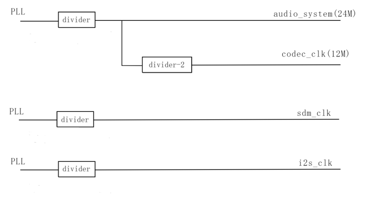
Audio initialization includes powering on the Audio module and initializing the Audio clock. The Audio clock comes from the system clock or PLL crossover. For example, using the PLL clock (see diagram above), the Audio clock is configured through audio_set_audio_clk interface. The audio clock of each chip can refer to the corresponding chip's datasheet. The following code uses the TL721x as an example; initialization of the remaining chips is shown in the corresponding Audio Demo.
/*
* @brief This function serves to initial audio.
* @return none.
*/
void audio_init(void)
{
audio_power_on();
audio_set_audio_clk(1, sys_clk.pll_clk / 24);
}
//Example: Audio initialization
audio_init();
Audio ADC usage and basic configuration
Audio ADC configuration includes ADC MIC BIAS pin settings, data bit width, sampling rate, FIFO and DMA channel selection, and gain control. The configuration sequence of the Audio ADC is: Audio module initialization - > clock initialization - > ADC parameters and FIFO configuration - > DMA configuration and enablement, with gain adjustable at any time. After configuring DFIFO on the TC series, the hardware will loop data into software buffs without DMA configuration.
-
Audio ADC MIC BIAS Pin Settings
The diagram below shows the hardware schematic of the AMIC. To ensure the AMIC operates properly, it is necessary to supply the MIC BIAS voltage. Depending on the chip, some chips provide voltage via external GPIO, so a dedicated GPIO output high level is required; Some chips use CODEC to provide MIC BIAS. The hardware has already connected the AMIC's VDD to the corresponding pin of the CODEC, so no external GPIO is needed. As long as the input source is selected as AMIC, the driver will turn on the MIC BIAS voltage of the CODEC.
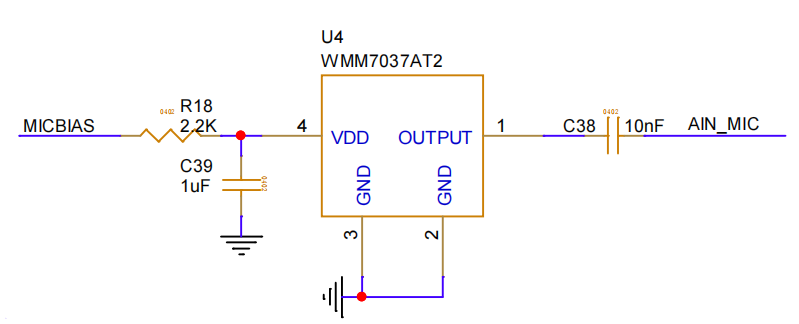
Example code for using external GPIO to provide MIC BIAS voltage is as follows:
/** * @brief Configure AMIC bias pins * @param[in] amic_bias - Biased pin (e.g., GPIO_PA0) */ void audio_set_amic_bias_pin(gpio_pin_e amic_bias); //Example: Enable AMIC bias audio_set_amic_bias_pin(GPIO_PA0);
Note
If the AMIC has no sound or abnormal sound, first check whether the MIC BIAS voltage is correct.
-
Audio ADC parameter configuration
ADC parameter configuration mainly includes selection of sampling rate, data bit width, FIFO channel, and DMA channel. Different chips have different configuration methods. The early chips TLSR825x/TLSR8359 and TLSR827x/TLSR8355 series configurations are as follows:
// TLSR825x/TLSR8359 and TLSR827x/TLSR8355 Example: Configure ADC FIFO and AMIC sampling rates audio_config_mic_buf((unsigned short*)MicBuf,MIC_BUFFER_SIZE); audio_amic_init(AUDIO_RATE_VAL);Except for early chips (TLSR825x/TLSR8359 and TLSR827x/TLSR8355) which specified the sampling rate at the initialization interface, other chips use structural packaging configuration parameters. For example, TL721x integrates these parameters into the structural
audio_codec_stream0_input_t, then usesaudio_codec0_input_init( input_config)Complete initialization. Example code is as follows. The parameters and initialization functions of configuration structures vary by chip. For details on each chip's configuration structure, please refer to the corresponding Audio Demo.audio_codec_stream0_input_t audio_codec_stream0_input = { .input_src = INPUT_SRC, // choose AMIC .sample_rate = SAMPLE_RATE, .data_width = DATA_WIDTH, .fifo_chn = RX_FIFO_NUM, .dma_num = RX_DMA_CHN, .data_buf = AUDIO_BUFF, .data_buf_size = sizeof(AUDIO_BUFF), }; /** * @brief This function serves to set codec initialization. * @param[in] audio_codec - audio_codec_stream0_input_t pointer. * @return none. */ void audio_codec_stream0_input_init(audio_codec_stream0_input_t *audio_codec) // Example: Initialize the audio ADC and configure ADC parameters audio_codec_stream0_input_init(&audio_codec_stream0_input); // Configure chain-linked DMA audio_rx_dma_chain_init(audio_codec_stream0_input.fifo_chn, audio_codec_stream0_input.dma_num, (unsigned short *)audio_codec_stream0_input.data_buf, audio_codec_stream0_ input.data_buf_size); // Enable Codec pathways and DMA audio_codec_stream0_input_en(audio_codec_stream0_input.dma_num); audio_codec_input_path_en(audio_codec_stream0_input.fifo_chn); -
Audio ADC gain configuration
Audio ADC gain configurations are divided into analog gain and digital gain. Analog gain is used to adjust the amplification of the PGA (Programmable Gain Amplifier), while digital gain compensates for the sampled data in the digital domain. The gain adjustment interface functions, range, and step vary by chip. For specific implementations, refer to the driver code. The following gain control interface is taken as an example of the TL721x.
- Analog Gain (PGA):
- Interface:
audio_set_adc_pga_gain (pga_gain). - Enumerate:
codec_in_pga_gain_e - Range: 0 dB ~ 45 dB (0 dB, 9 dB, 12 dB, 15 dB... 45 dB)
- Interface:
- Digital gain:
- Interface:
audio_set_stream0_dig_gain (d_gain). - Enumerate:
codec_in_path_digital_gain_e - Range: -48 dB ~ +42 dB, stepping 6 dB
- Interface:
- Analog Gain (PGA):
Audio DAC usage and basic configuration
Audio DAC configuration includes data bit width, sampling rate, FIFO and DMA channel selection, and gain control.
-
Audio DAC configuration parameters
DAC parameter configuration mainly includes sampling rate, data bit width, selection of FIFO channels, and DMA channels. Currently, all chips supporting DAC functionality are TL series chips, while TC series chips do not have DAC modules. In TLSR921x/TLSR951x, parameter initialization and configuration of the Audio DAC are performed via the
audio_initinterface. The configuration sequence of the Audio DAC is: Audio module initialization - > clock initialization - > DAC parameters and FIFO configuration - > DMA configuration and enablement, with gain adjustable at any time.// Example: Initialize the audio DAC channel and configure DAC parameters audio_init(BUF_TO_LINE_OUT, AUDIO_16K, MONO_BIT_16);Subsequent chips configure the packaging parameters of the structure. For example, in TLSR922x/TLSR952x, the parameters of the Audio DAC are described through
the audio_codec_output_tstructure and unified through theaudio_codec_stream_output_initinterface.audio_codec_output_t audio_codec_output = { .output_src = CODEC_DAC_STEREO, .sample_rate = AUDIO_48K, .fifo_num = FIFO0, .data_width = CODEC_BIT_16_DATA, .dma_num = TX_DMA_CHN, .mode = HP_MODE, .data_buf = sin_48k_stereo, .data_buf_size = sizeof(sin_48k_stereo), }; // Example: Initialize the audio DAC and configure DAC parameters audio_codec_stream_output_init(&audio_codec_output); -
Audio DAC gain configuration
DAC gain configurations are divided into two parts: analog gain and digital gain. The gain configuration interface, configuration range, and stepper vary by chip. Below, the use of the TLSR922x/TLSR952x is used as examples to describe the use of the gain Audio DAC control interface.
- Analog Gain (PGA):
- Interfaces:
audio_set_dac_pga_l_gain (pga_gain)(left channel) /audio_set_dac_pga_r_gain (pga_gain)(right channel) - Enumerate:
codec_out_pga_gain_e - Range: -60.2 dB ~ +6 dB (nonlinear levels: -60.2 dB, -54.2 dB, -48.2 dB...-6 dB, -3 dB, 0 dB, 3 dB, 6 dB)
- Stepping: Nonlinear, about 3 dB/6 dB steps.
- Interfaces:
- Digital gain:
- Interfaces:
audio_set_dac_l_gain (d_gain)(left channel) /audio_set_dac_r_gain (d_gain)(right channel) - Enumerate:
codec_out_path_digital_gain_e - Range: -72.2 dB ~ 0 dB (nonlinear levels: -72.2 dB, -66.2 dB, -60.2 dB...-6 dB, -3 dB, -1 dB, 0 dB)
- Step: Nonlinear
- Interfaces:
- Analog Gain (PGA):
Audio DMIC usage and basic configuration
Audio DMIC configuration includes DMIC pin configuration, data bit width, sampling rate, FIFO and DMA channel selection, and gain control. The configuration sequence of the CODEC DAC is: Audio module initialization -> clock initialization -> DMIC parameters and FIFO configuration -> DMA configuration and enablement, with gain adjustable at any time. After configuring DFIFO on the TC series, the hardware will loop data into software buffs without DMA configuration.
-
Audio DMIC pin settings
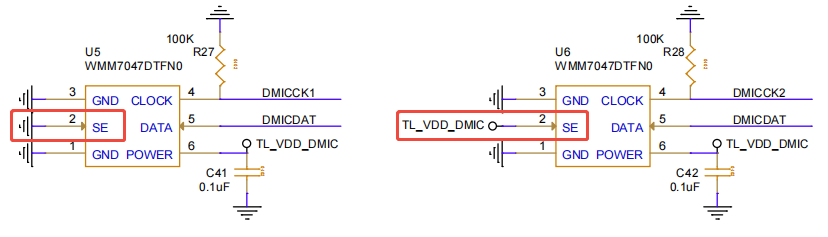
The DMIC power supply is provided by hardware; the DMIC clock drives the digital microphone's data output; the SE pin of the DMIC is grounded or connected to VDD to distinguish left and right channels; and the DMICDAT is the data output pin of the DMIC device. SE connected to GND (low level): Microphone is left channel L, data outputs effective PDM data on the rising edge of CLK; SE connected to VDD (High Level): The microphone is the right channel R, and the data outputs effective PDM data on the lower edge of the CLK. Taking the TL721x as an example, the DMIC pin configuration interface is
audio_set_stream0_dmic_pin.// DMIC pin configuration example audio_set_stream0_dmic_pin(GPIO_FC_PA2, GPIO_FC_PA3, GPIO_FC_PA4); -
Audio DMIC Parameter Configuration
DMIC parameter configuration mainly includes sampling rate, bit width, FIFO channel selection, and DMA channel configuration. The DMIC parameter configuration methods vary depending on the chip. For details, see the DMIC usage demo for the corresponding chip. The following uses the TL721x chip as an example.
audio_codec_stream0_input_t audio_codec_stream0_input = { .input_src = INPUT_SRC, // Select DMIC .sample_rate = SAMPLE_RATE, .data_width = DATA_WIDTH, .fifo_chn = RX_FIFO_NUM, .dma_num = RX_DMA_CHN, .data_buf = AUDIO_BUFF, .data_buf_size = sizeof(AUDIO_BUFF), }; // Example of DMIC channel initialization audio_codec_stream0_input_init(&audio_codec_stream0_input); -
Audio DMIC gain configuration
Since the DMIC is a digital microphone, its gain configuration only includes the digital gain section. The DMIC digital gain control interface varies among different chips. For details, see the driver code for the respective chip. Below, we use the TL721x chip as an example.
- Digital gain:
- Interface:
audio_set_stream0_dig_gain (d_gain). - Enumerate:
codec_in_path_digital_gain_e - Range: -48dB ~ +42B, stepping 6dB
- Interface:
- Digital gain:
Audio I2S usage and basic configuration
The I2S configuration sequence is: Audio module initialization - > clock initialization - > I2S parameters and FIFO configuration - > DMA configuration and enable. After configuring DFIFO on the TC series, the hardware loops data into the software buff without DMA configuration.
-
Audio I2S pin configuration
The I2S pin configuration includes bit clock lines, word selection lines, and TX and RX data lines. Taking the TL721x as an example, the I2S pin configuration is packaged into the
structure i2s_pin_config_tand unified throughi2s_set_pininterfaces. For the other chip configurations, refer to the corresponding chip's Audio Demo.i2s_pin_config_t i2s_pin_config = { .bclk_pin = GPIO_FC_PD5, // clock bits .adc_lr_clk_pin = GPIO_FC_PB3,//For RX characters, select PIN .dac_lr_clk_pin = GPIO_FC_PB4,//For TX, select PIN .adc_dat_pin = GPIO_FC_PB5, // RX DATA PIN .dac_dat_pin = GPIO_FC_PB6, // TX DATA PIN }; /** * @brief This function configures i2s pin. * @param[in] i2s_select - channel selection * @param[in] config - i2s config pin struct. * @return none. */ void i2s_set_pin(audio_i2s_select_e i2s_select, i2s_pin_config_t *config) -
Audio I2S crossover factor configuration
As shown in the clock diagram of the Audio module earlier, the I2S clock comes from the PLL division. The I2S frequency division system is managed uniformly by i2s_clk_config arrays. When PLL is 2400000000 (240M), and i2s_clk_config[5] = {4,1875,0,32,32}, the calculation formulas for each i2s clock are as follows:
I2S_CLK = 240000000(i2s_clk_config[0]/i2s_clk_config[1]) = 240000000(4/1875) = 512000
Note
i2s_clk_config[1] must be greater than or equal to twice the i2s_clk_config[0].
When i2s_clk_config[2] is 0, I2S_BCLK = I2S_CLK = 512000
When i2s_clk_config[2] is not 0, I2S_BCLK = I2S_CLK / (2 *[i2s_clk_config 2])
I2S_ADC_LR_CLK = I2S_BCLK / (i2s_clk_config[3]) = 512000 / 32 = 16000
I2S_DAC_LR_CLK = I2S_BCLK / (i2s_clk_config[4]) = 512000 / 32 = 16000
-
Audio I2S parameter configuration
I2S parameter configuration mainly includes sampling rate, bit width, FIFO channel selection, and DMA channel configuration. The I2S configuration methods vary by chip. For details, see the corresponding chip's I2S usage demo. The following example uses the TL721x chip.
audio_i2s_config_t audio_i2s_config = { .i2s_select = I2S2, .i2s_mode = I2S_I2S_MODE, .pin_config = &i2s_pin_config, .data_width = I2S_BIT_24_DATA, .master_slave_mode = I2S_AS_MASTER_EN, .sample_rate = (unsigned short *)&audio_i2s_48k_config[0], }; //I2S input parameter configuration audio_i2s_input_output_t audio_i2s_input = { .i2s_select = audio_i2s_config.i2s_select, .data_width = audio_i2s_config.data_width, .i2s_ch_sel = I2S_CHANNEL_STEREO, .fifo_chn = FIFO0, .dma_num = DMA0, .data_buf = AUDIO_BUFF, .data_buf_size = sizeof(AUDIO_BUFF), }; //I2S output parameter configuration audio_i2s_input_output_t audio_i2s_output = { .i2s_select = audio_i2s_config.i2s_select, .data_width = audio_i2s_config.data_width, .i2s_ch_sel = I2S_CHANNEL_STEREO, .fifo_chn = FIFO0, .dma_num = DMA0, .data_buf = AUDIO_BUFF, .data_buf_size = sizeof(AUDIO_BUFF), }; //Example of I2S input initialization configuration, this interface configures pins and clock crossover coefficients for I2S audio_i2s_config_init(&audio_i2s_config); //Example of I2S input initialization configuration audio_i2s_input_init(&audio_i2s_input); //Example of I2S output initialization configuration audio_i2s_output_init(&audio_i2s_output); //I2S clock enabled audio_i2s_clk_en(audio_i2s_config.i2s_select);
Audio SDM usage and basic configuration
-
Audio SDM pin configuration
Each SDM output needs to be configured with P and N pins, corresponding to the channel's positive and negative terminals. For detailed configuration methods for different chip series, see the corresponding Audio demo. Taking the TL721x as an example, the configuration of the SDM P/N pins is encapsulated in the
sdm_pin_config_tstructure and configured via theaudio_set_sdm_pininterface.
TL721x example:
typedef struct
{
gpio_func_pin_e sdm0_p_pin; // SDM0 positive pin
gpio_func_pin_e sdm0_n_pin; // SDM0 negative pin
gpio_func_pin_e sdm1_p_pin; // SDM1 positive pin
gpio_func_pin_e sdm1_n_pin; // SDM1 negative pin
} sdm_pin_config_t;
sdm_pin_config_t sdm_pin_config = {
.sdm0_p_pin = GPIO_FC_PA0,
.sdm0_n_pin = GPIO_FC_PA1,
.sdm1_p_pin = GPIO_FC_PF4,
.sdm1_n_pin = GPIO_FC_PF5,
};
audio_set_sdm_pin(&sdm_pin_config);
Note
The SDM0_P in the TL721x Demo uses the PA0 pin, which conflicts with the default DEBUG print pin. If using the SDM function, you need to change the 'DEBUG_INFO_TX_PIN' in 'printf.h' to another pin. Distribute the SDM pins on both sides of the EVB board to prevent signal interference and noise.
-
Audio SDM parameter configuration
SDM output parameters are configured through the
audio_codec_output_tstructure, including key parameters such as output channels, sampling rate, data bit width, and DMA channels. Taking the TL721x as an example, the rest of the chip refers to the corresponding driver code and Audio Demo.
TL721x example:
audio_codec_output_t structure definition:
typedef struct
{
void *data_buf; // Outputs a pointer to the data buffer
unsigned int data_buf_size; // Output data buffer size
audio_stream_output_src_e output_src; // Output source selection
unsigned char sample_rate; // Sampling rate
unsigned char data_width; // Data bit width
dma_chn_e dma_num; // DMA channel number
} audio_codec_output_t;
// Configuration example
#define SAMPLE_RATE AUDIO_48K
#define DATA_WIDTH CODEC_BIT_16_DATA
#define TX_FIFO_NUM FIFO0 // SDM fixedly uses FIFO0
#define TX_DMA_CHN DMA1
audio_codec_output_t audio_stream_output = {
.output_src = SDM_MONO, // or SDM_STEREO
.sample_rate = SAMPLE_RATE,
.data_width = DATA_WIDTH,
.dma_num = TX_DMA_CHN,
.data_buf = audio_tx_buff, // Output data buffer
.data_buf_size = sizeof(audio_tx_buff),
};
// SDM output initialization
audio_codec_stream_output_init(&audio_stream_output);
!!! note Important Note
The SDM module **only supports 16-bit data bit width**; `CODEC_BIT_16_DATA` must be used during configuration. Using other bit widths may cause output abnormalities. SDM output is fixed to **TX FIFO0**.
-
Audio SDM gain configuration
The Audio SDM module configures output gain through
audio_set_ascl_gain. For TL721x as an example, the rest of the chip refers to the corresponding Audio Demo and driver files.
TL721x example:
- Digital gain:
- Interface:
audio_set_ascl_gain (d_gain). - Enumerate:
ascl_out_path_digital_gain_e - Range: -48dB ~ +42B, stepping 6dB
- Interface:
Introduction to Audio's DMA chain
The audio module's data transmission relies heavily on DMA (Direct Memory Access) to efficiently transfer audio data between memory and the FIFO, reducing CPU overhead. Audio DMA uses a chained transmission mechanism to achieve data-loop buffering and ensure the continuity of audio streams.
The positional relationship between DMA and FIFO is shown in the figure below:
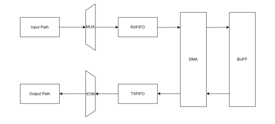
Important Notes
Once DFIFO is configured, the TC series chips automatically cycle audio data to the defined buffers, whereas TL series chips require configuring chain transmission via the DMA interface.
DMA chain transmission principle
DMA-linked transfer links multiple DMA transmission nodes via a linked list structure. After the current node completes transmission, it automatically jumps to the next node, forming a loop.
This diagram shows DMA dual-node chain transmission, while Audio Demos typically use single-node chain transmission.
+-------------+ +-------------+ +-------------+
| DMA Node 0 | --> | DMA Node 1 | --> | DMA Node 0 | (Loop)
+-------------+ +-------------+ +-------------+
| | |
Buff[0] Buff[1] Buff[0]
Advantages of chain transmission:
- Continuous transmission: Enables uninterrupted audio data streaming without CPU intervention
- Dual buffering mechanism: Using dual-node linked list loops to achieve ping-pong buffering and avoid data overwrite
- Low-latency: DMA hardware automatically handles data transfer, providing fast response times
Audio DMA configuration structure
The Audio driver predefines DMA configurations for RX (receive) and TX (transmit):
RX DMA configuration (audio_dma_rx_config):
| Field | Configuration values | Description |
|---|---|---|
| dst_req_sel | 0 | Since it is the RX request source, this value is 0 |
| src_req_sel | DMA_REQ_AUDIO_RX | Audio RX FIFO request source |
| dst_addr_ctrl | DMA_ADDR_INCREMENT | Destination Address Increment (Memory Buffer) |
| src_addr_ctrl | DMA_ADDR_FIX | Source Address Fixed (FIFO Register) |
| dstmode | DMA_NORMAL_MODE | Normal mode |
| srcmode | DMA_HANDSHAKE_MODE | Source handshake mode (waiting for FIFO request) |
| dstwidth / srcwidth | DMA_CTR_WORD_WIDTH | Transfer width is Word (32bit) |
| src_burst_size | 0 | It must be 0 |
TX DMA Configuration (audio_dma_tx_config):
| Field | Configuration values | Description |
|---|---|---|
| dst_req_sel | DMA_REQ_AUDIO_TX | Audio TX FIFO request source |
| src_req_sel | 0 | Since it is the TX request source, this value is 0 |
| dst_addr_ctrl | DMA_ADDR_FIX | Fixed Target Address (FIFO Register) |
| src_addr_ctrl | DMA_ADDR_INCREMENT | Source address increases (memory buffer) |
| dstmode | DMA_HANDSHAKE_MODE | Target handshake mode |
| srcmode | DMA_NORMAL_MODE | Normal mode |
| dstwidth / srcwidth | DMA_CTR_WORD_WIDTH | Transfer width is Word (32bit) |
| src_burst_size | 0 | It must be 0 |
Audio DMA linked transmission interface
- Audio RX DMA chain initialization
/**
* @brief Initialize Audio RX DMA chain transfer
* @param[in] rx_fifo_chn - RX FIFO channel selection
* @param[in] chn - DMA channel number
* @param[in] in_buff - Receive data buffer pointer (must be 4-byte aligned)
* @param[in] buff_size - buffer size (bytes, must be multiples of 4, maximum 0x10000)
*/
void audio_rx_dma_chain_init(audio_fifo_chn_e rx_fifo_chn, dma_chn_e chn,
unsigned short *in_buff, unsigned int buff_size);
- Audio TX DMA chain initialization
/**
* @brief Initialize Audio TX DMA chain transfer
* @param[in] tx_fifo_chn - TX FIFO channel selection
* @param[in] chn - DMA channel number
* @param[in] out_buff - Send data buffer pointer (must be 4-byte alignment)
* @param[in] buff_size - buffer size (bytes, must be multiples of 4, maximum 0x10000)
*/
void audio_tx_dma_chain_init(audio_fifo_chn_e tx_fifo_chn, dma_chn_e chn,
unsigned short *out_buff, unsigned int buff_size);
- Audio DMA enables and disables
// Enable RX DMA
static inline void audio_rx_dma_en(dma_chn_e chn);
// Disable RX DMA
static inline void audio_rx_dma_dis(dma_chn_e chn);
// Enable TX DMA
static inline void audio_tx_dma_en(dma_chn_e chn);
// Disable TX DMA
static inline void audio_tx_dma_dis(dma_chn_e chn);
Audio DMA chain underlying implementation
RX DMA chain initialization process:
void audio_rx_dma_chain_init(audio_fifo_chn_e rx_fifo_chn, dma_chn_e chn,
unsigned short *in_buff, unsigned int buff_size)
{
audio_rx_fifo_chn = rx_fifo_chn;
// 1. Configure DMA channel parameters
audio_rx_dma_config(chn, in_buff, buff_size, &g_audio_rx_dma_list_cfg[rx_fifo_chn]);
// 2. Add linked list elements (self-looping, enabling single-buffered loop transmission)
audio_rx_dma_add_list_element(&g_audio_rx_dma_list_cfg[rx_fifo_chn],
&g_audio_rx_dma_list_cfg[rx_fifo_chn],
in_buff, buff_size);
}
TX DMA chain initialization process:
void audio_tx_dma_chain_init(audio_fifo_chn_e tx_fifo_chn, dma_chn_e chn,
unsigned short *out_buff, unsigned int buff_size)
{
audio_tx_fifo_chn = tx_fifo_chn;
// 1. Configure DMA channel parameters
audio_tx_dma_config(chn, out_buff, buff_size, &g_audio_tx_dma_list_cfg[tx_fifo_chn]);
// 2. Add linked list elements (self-looping, enabling single-buffered loop transmission)
audio_tx_dma_add_list_element(&g_audio_tx_dma_list_cfg[tx_fifo_chn],
&g_audio_tx_dma_list_cfg[tx_fifo_chn],
out_buff, buff_size);
}
Use examples
// Enter the configuration
audio_rx_dma_chain_init(FIFO0, DMA0, (unsigned short *)audio_buff, sizeof(audio_buff));
audio_rx_dma_en(DMA0);
// Output configuration
audio_tx_dma_chain_init(FIFO0, DMA1, (unsigned short *)audio_buff, sizeof(audio_buff));
audio_tx_dma_en(DMA1);
Audio FIFO interrupted
The Audio module provides an independent interrupt mechanism for each FIFO channel. When the FIFI's data volume reaches a preset threshold, an interrupt is triggered, allowing users to process audio data or monitor status within the interrupt service routine.
FIFO interrupt type
The Audio module supports two types of FIFO interrupts: RX and TX. For example, with the TL721x, it has 3 RX FIFOs and 3 TX FIFOs, resulting in the following 6 FIFO interrupts:
typedef enum
{
AUDIO_RX_FIFO0_IRQ = BIT(0), // RX FIFO0 interrupt
AUDIO_RX_FIFO1_IRQ = BIT(1), // RX FIFO1 interrupt
AUDIO_RX_FIFO2_IRQ = BIT(2), // RX FIFO2 interrupt
AUDIO_TX_FIFO0_IRQ = BIT(3), // TX FIFO0 interrupt
AUDIO_TX_FIFO1_IRQ = BIT(4), // TX FIFO1 interrupt
AUDIO_TX_FIFO2_IRQ = BIT(5), // TX FIFO2 interrupt
} audio_fifo_irq_type_e;
FIFO interrupt trigger principle
FIFO interrupts are triggered based on a threshold mechanism:
- RX FIFO Interrupt: Triggered when the amount of data received in the RX FIFO reaches or exceeds a set threshold
- TX FIFO Interrupt: Triggered when the amount of data sent in the TX FIFO reaches or exceeds a set threshold
The threshold is configured through the following interface:
/**
* @brief Set the RX FIFO interrupt threshold
* @param[in] rx_fifo_chn - RX FIFO channel
* @param[in] threshold - threshold (number of bytes), the actual value written to the register is threshold >> 2
*/
static inline void audio_set_rx_fifo_threshold(audio_fifo_chn_e rx_fifo_chn, unsigned short threshold);
/**
* @brief Set TX FIFO interrupt threshold
* @param[in] tx_fifo_chn - TX FIFO channel
* @param[in] threshold - threshold (number of bytes), the actual value written to the register is threshold >> 2
*/
static inline void audio_set_tx_fifo_threshold(audio_fifo_chn_e tx_fifo_chn, unsigned short threshold);
Notes
Threshold registers are in Word (4 bytes), so the actual threshold = configuration value × 4. For example, configuring 'AUDIO_BUFF_SIZE / 2' means an interrupt is triggered when the FIFO data volume reaches half of the buffer.
FIFO interrupt control interface
Enable FIFO interrupts:
/**
* @brief Enables RX FIFO interrupts
* @param[in] rx_fifo_chn - RX FIFO channel
*/
static inline void audio_rxfifo_irq_en(audio_fifo_chn_e rx_fifo_chn);
/**
* @brief Enable TX FIFO interrupts
* @param[in] tx_fifo_chn - TX FIFO channel
*/
static inline void audio_txfifo_irq_en(audio_fifo_chn_e tx_fifo_chn);
Query and clear interrupt status:
/**
* @brief Obtain the FIFO interrupt status
* @param[in] irq_status - Interrupt type
* @return Interrupt status; non-0 indicates the corresponding interrupt is triggered
*/
static inline unsigned char audio_get_irq_status(audio_fifo_irq_type_e irq_status);
/**
* @brief Clear the FIFO interrupt state
* @param[in] irq_status - Interrupt type
*/
static inline void audio_clr_irq_status(audio_fifo_irq_type_e irq_status);
For examples of FIFO interrupts usage, refer to the AUDIO_FIFO_IRQ_TEST case in the TL721x Audio Demo.
Common FIFO pointer and DMA pointer query interfaces
During FIFO interrupt handling or debugging, the positions of FIFO and DMA pointers can be obtained through the following interfaces:
| Interface | Function |
|---|---|
audio_get_rx_wptr(rx_fifo_chn) |
Get the RX FIFO write pointer |
audio_get_tx_rptr(tx_fifo_chn) |
Get the TX FIFO read pointer |
audio_get_rx_dma_wptr(dma_chn) |
Obtain the RX DMA target address |
audio_get_tx_dma_rptr(dma_chn) |
Obtain the TX DMA source address |
SPI
Overview
Standard SPI interface
The Serial Peripheral Interface (SPI) is a synchronous serial interface that allows embedded processors to communicate with peripheral devices and exchange data serially.
Standard SPI interfaces generally use 4-wire communication:
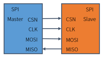
| Name | Meaning |
|---|---|
| CSN | Device chip selection signal line, low level effective |
| CLK | Clock signal line |
| MOSI | Master data output, Slave data input line |
| MISO | Master data input, Slave data output line |
SPI communication processes and four operating modes
The diagram below is a simple example of SPI communication:
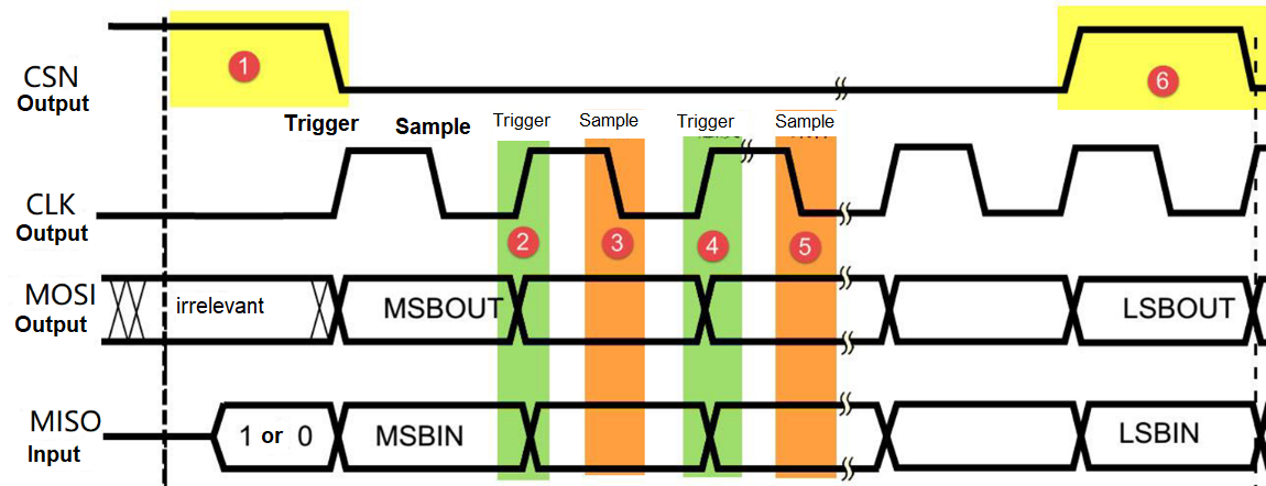
CSN, CLK, and MOSI signals are all generated by the Master, with data output via MOSI lines. The MISO signal is generated by the Slave, and the Master reads the data from the Slave. MOSI and MISO signals are valid only when CSN is low, and data is triggered on the rising or falling edge of CLK. In CLK, MOSI and MISO transmit 1 bit of data per clock cycle, so 1 byte of data can be transferred in 8 clock cycles.
Based on the difference between the idle CLK clock polarity (CPOL) and the sampling time (CLK clock phase CPHA), SPI distinguishes four operating modes:
| SPI operating mode | CPOL | CPHA |
|---|---|---|
| SPI_MODE0 | 0 | 0 |
| SPI_MODE1 | 0 | 1 |
| SPI_MODE2 | 1 | 0 |
| SPI_MODE3 | 1 | 1 |
- CPOL=0: CLK remains low during idle moments; CPOL=1: CLK maintains a high level during idle moments.
- CPHA=0: Sampling is triggered at the odd edge of the CLK; CPHA=1: Sampling is triggered at the even-numbered edge of the CLK.
The Master and Slave must operate in the same mode to communicate normally.
Diverse SPI interfaces
Based on the standard SPI, to adapt to different application scenarios, many categories of SPI interfaces have gradually emerged:
-
3-line SPI: Only 3 wires (CLK, CSN, MOSI), sharing a single line for data transmission and reception, using half-duplex communication.
-
Dual SPI: Expands the use of MOSI and MISO to enable half-duplex operation, allowing data to be transmitted in both directions. MOSI becomes IO0, MISO becomes IO1, and can transmit 2 bits of data within one clock cycle.
-
Quad SPI: Expands the usage of WP and HOLD. WP becomes IO2, HOLD becomes IO3, and it has four data cables, capable of transmitting 4 bits per clock cycle.
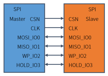
Overview of Chip SPI Resources
SPI type description
Different chips provide different types of SPI peripherals. Below is the distribution of each type across all platforms and the support for each chip's IO mode and DMA:
| Chips | PSPI | HSPI | LSPI | GSPI | SPI | Total | IO mode | DMA |
|---|---|---|---|---|---|---|---|---|
| TLSR921x/TLSR951x | ✅ 1 | ✅ 1 | — | — | — | 2 | Single/Dual (PSPI), Single/Dual/Quad (HSPI) | Yes |
| TLSR922x/TLSR952x | — | — | ✅ 1 | ✅ 1 | — | 2 | Single/Dual/Quad | Yes |
| TL721x / TL751x | — | — | ✅ 1 | ✅ 1 | — | 2 | Single/Dual/Quad/3-line | Yes |
| TL321x / TL323x | — | — | — | ✅ 1 | — | 1 | Single/Dual/Quad/3-line | Yes |
| TL322x | — | — | ✅ 1 | ✅5 | — | 6 | Single/Dual/Quad/3-line | Yes |
| TLSR820x/TLSR8373 | — | — | — | — | ✅ 1 | 1 | Single/Dual/Quad/3-line | Yes |
| TLSR825x/TLSR8359 / TLSR827x/TLSR8355 / TC321x / TC123x | — | — | — | — | ✅ 1 | 1 | Single | No |
Meanings of each type:
| SPI type | Full name | Bus | Description |
|---|---|---|---|
| SPI | System Bus | TC series unified SPI modules, TLSR820x/TLSR8373 series support Single/Dual/Quad/3-Line, while the others only support Single | |
| PSPI | APB SPI | APB | TLSR921x/TLSR951x series exclusive low-speed SPI, supports only Single/Dual |
| HSPI | AHB SPI | AHB | TLSR921x/TLSR951x series Exclusive high-speed SPI, supporting Single/Dual/Quad |
| LSPI | LCD SPI | AHB | Supports specific ramless screen drivers (LUT command table, porch timing, frame control) |
| GSPI | General SPI | AHB | General/high-speed SPI, supports XIP, usually with an AHB bus |
- TLSR921x/TLSR951x are the only chips named after
PSPI/HSPI. - The TL322x has 5 GSPI instances, making it the chip with the most GSPI applications.
- All TC series chips have only one SPI module, uniformly named
SPI, with no distinction between PSPI/HSPI/LSPI/GSPI.
Function description
Interface naming rules
- spi prefix: Interfaces that HSPI and PSPI / GSPI and LSPI can all use.
- PSPI prefix: For PSPI only.
- hspi prefix: for HSPI only.
- gspi prefix: for GSPI only.
- lspi prefix: For LSPI only.
- dma suffix: interface used in DMA mode.
- plus suffix: supports a wider variety of read/write modes and operation commands (common across TLSR921x/TLSR951x/TLSR922x/TLSR952x series and TL series).
For example, the spi_master_write_read_dma_plus interface uses a DMA channel, first writing the address to the SPI Slave, then reading data from the corresponding address on the SPI Slave.
About "read" and "write_read":
- Interfaces with the "read" field support hardware automatically sending address frames, suitable for applications where hardware address frames are enabled.
- Interfaces with the "write_read" are used when no hardware address frame is enabled. The address information must first be written to the SPI Slave via “write” before the corresponding address can be read..
Comparison of SPI module capabilities for each chip
The hardware support for commonly used protocol frames of each chip's SPI modules is as follows (Y=support, N=Not supported):
| SPI module | cmd_en | cmd_fmt | address_en | address_fmt | 3-line | Dual | Quad |
|---|---|---|---|---|---|---|---|
| TLSR820x/TLSR8373 | Y | Y | Y | Y | Y | Y | Y |
| TLSR921x/TLSR951x HSPI | Y | Y | Y | Y | Y | Y | Y |
| TLSR921x/TLSR951x PSPI | Y | N | N | N | Y | Y | N |
| TLSR922x/TLSR952x GSPI | Y | Y | Y | Y | Y | Y | Y |
| TLSR922x/TLSR952x LSPI | Y | Y | Y | Y | Y | Y | Y |
- cmd_en/cmd_fmt: Hardware cmd frames and their format follow Dual/Quad I/O encoding
- address_en/address_fmt: The hardware address frame and its format follow the Dual/Quad I/O encoding
- The GSPI/LSPI capability of the TL721x/TL321x/TL322x/TL323x/TL751x series is the same as that of the TLSR922x/TLSR952x series
- The TLSR820x/TLSR8373 series has the same capabilities as the TLSR921x/TLSR951x HSPI, while other TC chips (TLSR825x/TLSR8359/TLSR827x/TLSR8355/TC321x/TC123x) do not support hardware cmd/addr frame functions. The TC122x does not have an SPI module and only supports low-level MSPI interfaces for Flash operations.
Master mode
In Master mode, Telink SPI provides two types of interfaces:
| Category | suffix | Applicable scenarios | Features |
|---|---|---|---|
| Standard Master | No _plus |
Simple data transmission and reception, no need for cmd/addr frames | Simple interface, only data is transferred |
| Plus Master | _plus |
Flash, PSRAM, and other peripherals that require cmd/addr/dummy frames | Hardware automatically generates cmd/addr/dummy frames |
Both types of interfaces support both polling and DMA transmission modes (_dma suffix).
-
Standard SPI Master
No
_plussuffix, suitable for scenarios where pure data is transmitted only (such as direct communication between two MCUs).Initialization: TLSR921x/TLSR951x series use
spi_master_config(),TLSR922x/TLSR952x series and TLxx series (TL321x/TL323x/TL322x/TL721x/TL751x and later TL series) usespi_master_config_plus()And close cmd/addr.Read/write: The Master sends/receives data directly, without specifying cmd or address. Interfaces are selected via
spi_sel_eparameters for SPI modules (TLSR921x/TLSR951x seriesare HSPI_MODULE/PSPI_MODULE, TLSR922x/TLSR952x and TLxx seriesare GSPI_MODULE/LSPI_MODULE). -
Plus Master (advanced frame format)
_plussuffix: hardware supports automatic generation of cmd frames, address frames, dummy frames (empty period), and adapts to standard SPI peripherals such as Flash/PSRAM for command protocols.The data frame format is: [cmd] + [address] + [dummy] + data ([] means optional).
Step 1 — Configure the data frame format. The TLSR921x/TLSR951x series use independent hspi_config_st/pspi_config_t, while the TLSR922x/TLSR952x and TLxx series use a unified spi_wr_rd_config_t:
// TLSR921x/TLSR951x series
hspi_config_st config = {
.hspi_io_mode = HSPI_QUAD, .hspi_dummy_cnt = 6,
.hspi_cmd_en = 1, .hspi_addr_en = 1, .hspi_addr_len = 3,
.hspi_cmd_fmt_en = 0, .hspi_addr_fmt_en = 1,
};
hspi_master_config_plus(&config);
// TLSR922x/TLSR952x series and TLxx series
spi_wr_rd_config_t config = {
.spi_io_mode = SPI_QUAD_MODE, .spi_dummy_cnt = 6,
.spi_cmd_en = 1, .spi_addr_en = 1, .spi_addr_len = 3,
.spi_cmd_fmt_en = 0, .spi_addr_fmt_en = 1,
};
spi_master_config_plus(GSPI_MODULE, &config);
Meanings of each field:
| Field | Description |
|---|---|
spi_io_mode |
I/O modes: Single/Dual/Quad |
spi_dummy_cnt |
Number of empty cycles between cmd and data |
spi_cmd_en |
Whether the hardware sends cmd frames. When closed, the cmd parameter on the _plus interface is invalid |
spi_addr_en |
Whether the hardware sends the address frame |
spi_addr_len |
address: Number of frame bytes (1\~4) |
spi_cmd_fmt_en |
Whether the cmd frame format follow I/O mode (if not, always Single) |
spi_addr_fmt_en |
Whether the address frame format follows the I/O mode |
Step 2 — Call the Plus read/write interface. The interface is named spi_master_{action}_plus and supports polling and DMA (_dma suffix):
| Interface | Purpose |
|---|---|
spi_master_write_plus |
Send cmd + address + write data |
spi_master_read_plus |
Send cmd + address to receive data |
spi_master_write_read_plus |
Send cmd + address (software splicing) to receive data |
Differences: The _plus interface of the TLSR921x/TLSR951x series returns void, while the TLSR922x/TLSR952x and TLxx series return drv_api_status_e. The cmd parameter of the TL751x is unsigned short (16-bit), while the rest of the chip is unsigned char (8-bit).
-
Reading and writing methods
Read/write mode is used to indicate whether the operation requires dummy (empty period) frames, and whether the instruction operation should be read or written:
typedef enum {
SPI_MODE_WR_WRITE_ONLY = 1, // Write
SPI_MODE_WR_DUMMY_WRITE = 8, // dummy + write
} spi_wr_tans_mode_e;
typedef enum {
SPI_MODE_RD_READ_ONLY = 2, // Read (must enable CmdEn)
SPI_MODE_RD_DUMMY_READ = 9, // dummy + read
} spi_rd_tans_mode_e;
typedef enum {
SPI_MODE_WR_RD = 3, // Write + Read (must enable CmdEn)
SPI_MODE_WR_DUMMY_RD = 5, // Write + dummy + read
} spi_wr_rd_tans_mode_e;
For example, when reading data, if the SPI Slave requires dummy-free frames, the reading method should be SPI_MODE_RD_DUMMY_READ.
Slave mode
-
HSPI/PSPI/GSPI/LSPI Slave
The HSPI in the TLSR921x/TLSR951x series supports Single, Dual, and Quad I/O modes when used as Slaves; When PSPI is used as a Slave, it supports Single and Dual I/O modes. Both automatically parse cmd, but Slave data reception and sending require software operation.
Both the TLSR922x/TLSR952x series and the TLxx series GSPI/LSPI slaves support Single/Dual/Quad, using a unified
spi_slave_init (spi_sel, mode)initialization.
Slave communication frame format: cmd + dummy (n×clock) + data. The I/O mode and dummy clock count of Master and Slave must be consistent.
| I/O mode | Write/read | Data line mapping |
|---|---|---|
| Single | MOSI (IO0) sends cmd + data, MISO (IO1) is used only for reading data | 1 bit/cycle |
| Dual | IO0/IO1 transmit/receive simultaneously, splitting every 2 bits into two wires | 2 bits/cycle |
| Quad | IO0\~IO3 simultaneous send/receive (requires WP/IO2 and HOLD/IO3 configuration) | 4 bits/cycle |
HSPI/PSPI Slave Operation Instructions (Compatible with All Series):
// Write cmd (partial examples)
SPI_WRITE_DATA_SINGLE_CMD = 0x51 // Single write
SPI_WRITE_DATA_DUAL_CMD = 0x52 // Dual writes
HSPI_WRITE_DATA_QUAD_CMD = 0x54 // Quad writes (HSPI only)
// Read cmd (partial examples)
SPI_READ_DATA_SINGLE_CMD = 0x0B // Single read
SPI_READ_DATA_DUAL_CMD = 0x0C // Dual reads
HSPI_READ_DATA_QUAD_CMD = 0x0E // Quad reads (HSPI only)
Instructions with the SPI prefix HSPI and PSPI are interchangeable; instructions with the HSPI prefix are only usable by HSPI.
-
SPI Slave Module (Dedicated Hardware Slave)
All TL series chips include an independent SPI Slave module (distinct from the GSPI/LSPI Slave), in which hardware automatically parses read/write commands and operates on the corresponding addresses without software intervention. Only Single/Dual I/O is supported. Only Single/Dual I/O is supported.
Note
The 'spi_slave_set_pin()' of the TLSR921x/TLSR951x series and TLSR922x/TLSR952x series has no parameters (fixed pins TLSR921x/TLSR951x: PA1\~PA4, TLSR922x/TLSR952x: PC0~PC3); Other chips can be flexibly configured through 'spi_slave_set_pin(sspi_pin_config_t*)'.
Comparison between SSPI modules and GSPI/LSPI Slave:
| Type | Agreement | Data format | Features |
|---|---|---|---|
| GSPI/LSPI Slave | cmd + dummy + data | Flexible and software-controlled | Supports Quad, pins can be paired |
| SPI Slave Module (SSPI) | cmd + addr(32bit h -> l) + data | Hardware auto-parsing | Only Single/Dual, simple scenarios |
The address order of SSPI modules is high-byte first (addr(32-bit) high -> low), which differs from the GSPI/LSPI Slave’s cmd+dummy+data format.
Clock settings
-
Clock source
Master clock sources vary depending on the chip/module:
| Chips / Modules | Clock source | Configuration methods |
|---|---|---|
| TLSR921x/TLSR951x HSPI | hclk | Manually calculate the divider: sys_clk.hclk * 1,000,000 / (2 × SPI_CLK) - 1 |
| TLSR921x/TLSR951x PSPI | pclk | Manually calculate the divider: sys_clk.pclk * 1,000,000 / (2 × SPI_CLK) - 1 |
| TL751x series | Optional SRC_CLK_XTAL_48M, etc |
Manual specification |
| TLSR922x/TLSR952x and other TLxx series | PLL clock, automatic selection | sys_clk.pll_clk * 1000000 / SPI_CLK |
Initialization example:
spi_master_init(GSPI_MODULE, sys_clk.pll_clk * 1000000, 3000000);
SPI_CLK going beyond the configuration range may cause communication failures. The maximum supported SPI clock varies by chip and is based on the header file comment.
-
Slave clock
The Slave clock is input by the Master and does not require manual configuration. Constraint:
F_Master ≤ F_source_slave ÷ 4(F_source_slaveis the internal clock source frequency of the Slave chip); otherwise, the Slave may not sample correctly.
interrupt
The SoC supports various SPI interrupt types and can be flexibly configured for different application scenarios.
| Modes | interrupt | Description | Abnormal interruption | Manual removal is required | Generation Party |
|---|---|---|---|---|---|
| Not DMA | SPI_RXF_OR_INT | RX FIFO over run: When received, the program read is not fast enough, and the RX FIFO is overwritten | Y | Y | Slave |
| Not DMA | SPI_TXF_UR_INT | TX FIFO under run: program writing is not fast enough during transmission, resulting in interrupted transmission | Y | Y | Slave |
| Not DMA | SPI_RXF_INT | RX FIFO Threshold Interrupt: RX FIFO data reaches/exceeds thresholds | N | Y | Master/Slave |
| Not DMA | SPI_TXF_INT | TX FIFO threshold interrupt: TX FIFO data is less than/reaches the threshold | N | Y | Master/Slave |
| DMA/Non-DMA | SPI_END_INT | Data transmission ends and is interrupted, completing a data transfer | N | Y | Master/Slave |
| DMA/Non-DMA | SPI_SLV_CMD_INT | In Slave mode, triggered every 1 Byte command received | N | Y | Slave |
Note
The interrupt state enumeration bit offset of the TLSR921x/TLSR951x series differs from TLSR922x/TLSR952x and TLxx series: in the TLSR921x/TLSR951x series, 'SPI_END_INT = BIT(6)', and in TLSR922x/TLSR952x and TLxx series, 'SPI_END_INT = BIT(4)'. When porting code across chips, be sure to check the definition of interrupt status bits.
Interrupt Enable and State Queries:
// Enable the interrupt
spi_set_irq_mask(SPI_MODULE_SEL, SPI_END_INT_EN | SPI_RXFIFO_INT_EN);
// Query the interrupt status
u8 status = spi_get_irq_status(SPI_MODULE_SEL);
if (status & SPI_END_INT) {
spi_clr_irq_status(SPI_MODULE_SEL, SPI_END_INT);
// Processing transmission complete
}
DMA mode
TLSR921x/TLSR951x series uses macro definitions to select DMA channels:
#define TX_DMA_CHN DMA2
#define RX_DMA_CHN DMA3
hspi_set_tx_dma_config(TX_DMA_CHN);
hspi_set_rx_dma_config(RX_DMA_CHN);
TLSR922x/TLSR952x and TLxx series configure structures using DMA:
spi_set_tx_dma_config(GSPI_MODULE, DMA2);
spi_set_master_rx_dma_config(GSPI_MODULE, DMA3);
Methods to determine whether data has been sent or received in DMA mode:
- Query method:
spi_is_busy(spi_sel)— returns busy status - Interrupt method:
spi_set_irq_mask(SPI_MODULE_SEL, SPI_END_INT_EN)— Enable END interrupts
DMA usage notes (universal across platforms):
SPI_END_INTinterrupt does not mean data transmission is complete (it only means FIFO data transfer is complete, CSN is not raised). After aSPI_END_INTinterrupt occurs, the busy signal is queried again until IDLE is reached, marking the end.- When using DMA for transmission, the send/receive struct or array must be aligned with four bytes (as shown in the demo by
__attribute__((aligned(4))). - When using DMA to receive SPI data into the buffer, the destination buffer size must be a multiple of 4. The reason is that each DMA sends 4 bytes to the Buffer, and even if the configured read length is less than 4, it will write 4 bytes to the destination address. For example, define the array buffer size as 5 bytes, configure the DMA to read 5 bytes from SPI into the buffer, and the DMA actually transfers 8 bytes to the buffer twice, with the extra 3 bytes possibly overwriting other variables. In this case, the array size should be configured to 8 Bytes.
- The DMA configurations in the TLSR922x/TLSR952x and TLxx series are divided into three independent configurations:
tx/master_rx/slave_rx. The TLSR921x/TLSR951x series usestx/rxconfigurations.
3-Line mode
The HSPI/PSPI Master/Slave of the TLSR921x/TLSR951x series, as well as the GSPI/LSPI of TLSR922x/TLSR952x and TLxx series, all support 3-Line mode.
Note
The TLSR922x/TLSR952x series only supports 3-Line with GSPI; LSPI does not.
The interface called is:
void spi_set_3line_mode(spi_sel_e spi_sel)
3-Line mode read/write instructions are compatible with HSPI/PSPI/GSPI/LSPI for SINGLE_CMD.
Multi-SPI Slave structure
For multi-SPI Slave applications, each Slave's CSN pin can be assigned to it. Once a data transfer is complete, the CSN will be incremented, and you can switch the CSN to simulate switching to a Slave.
TLSR921x/TLSR951x series HSPI Master calls the interface:
void hspi_cs_pin_dis(hspi_csn_pin_def_e pin);
void hspi_cs_pin_en(hspi_csn_pin_def_e pin);
TLSR922x/TLSR952x and TLxx series GSPI Master supports multiple CSNs (GSPI_XIP0\~3), enabling multiple Slaves through XIP configuration or direct GPIO operations.
XIP mode
XIP (eXecute In Place) refers to on-chip execution, allowing applications to directly fetch, decode, and execute from external storage devices. XIP can extend the SoC's address space to external storage devices.
- Chips supported by XIP
| Chips | GSPI XIP | LSPI XIP | Number of XIP channels |
|---|---|---|---|
| TLSR921x/TLSR951x HSPI | ✅ | — | 1 |
| TLSR922x/TLSR952x | ✅ | — | 4 (XIP0\~3) |
| TL721x | ✅ | ✅ | 4 |
| TL322x | ✅ | ✅ | 4 |
| TL321x | ✅ | ✅ | 4 |
| TL323x | ✅ | ✅ | 4 |
- TLSR921x/TLSR951x series XIP configuration
hspi_xip_seq_mode_en(); // Enable sequential mode
hspi_xip_page_size(4); // Set the page size
hspi_xip_en(); // Enable XIP
The seq_mode (sequential mode) in the TLSR921x/TLSR951x series refers to a sequential mode that divides data into blocks of \(2^{page\_size}\) Bytes for interval transmission. Each block is sent/sent and then sent again, increasing the CS once.
Send Instructions and Data Read/Write:
void hspi_master_write_xip_cmd_data(u8 cmd, u32 addr_offset, u8 data_in, spi_wr_tans_mode_e wr_mode);
void hspi_master_write_xip(u8 cmd, u32 addr_offset, u8 *data, u32 data_len, spi_wr_tans_mode_e wr_mode);
void hspi_master_read_xip(u8 cmd, u32 addr_offset, u8 *data, u32 data_len, spi_rd_tans_mode_e rd_mode);
TLSR921x/TLSR951x series XIP on-chip executor — switch the PC pointer to the corresponding address of the XIP device (base address 0x1000000 + relative address 0x00) via the following two commands:
__asm__("li t0,0x1000000");
__asm__("jarr t0");
- TLSR922x/TLSR952x and TLxx series XIP configurations
The TLSR922x/TLSR952x and TLxx series use a unified spi_xip_config_t structure and support a richer range of configuration options:
spi_xip_config_t xip_config = {
// Read the configuration
.spi_xip_rd_io_mode = SPI_QUAD_MODE,
.spi_xip_rd_addr_len = 2, // 3-byte address (2 = 3 - 1)
.spi_xip_rd_addr_en = 1,
.spi_xip_rd_cmd_en = 1,
.spi_xip_rd_dummy_cnt = 3, // 4 dummy cycles (3 = 4 - 1)
.spi_xip_rd_transmode = SPI_MODE_WRITE_DUMMY_READ,
.spi_xip_rd_cmd = 0x0B, // Fast Read command
.spi_xip_wr_io_mode = SPI_QUAD_MODE,
// ... Write configurations are similar
.spi_3_line_en = 0,
};
spi_master_init(GSPI_MODULE, 48000000, 3000000);
gspi_set_xip_pin(&xip_pin_config);
gspi_xip_end_addr_set();
gspi_set_xip_config(GSPI_XIP0, &xip_config);
spi_xip_en(GSPI_MODULE);
The GSPI XIP base addresses for the TLSR922x/TLSR952x and TLxx series are 0x88000000 and support 4 XIP regions:
- XIP0: 0x88000000 \~ 0x88ffff00
- XIP1: 0x89000000 \~ 0x89ffff00
- XIP2: 0x8a000000 \~ 0x8affff00
- XIP3: 0x8b000000 \~ 0x8bffff00
Demo example
TL Series Demo
| Demo version | Path | Applicable chips |
|---|---|---|
| V1.0 | demo/vendor/SPI_Demo/SPI_V1.0/ |
TLSR921x/TLSR951x |
| V1.1 | demo/vendor/SPI_Demo/SPI_V1.1/ |
TLSR922x/TLSR952x / TL721x / TL321x / TL751x / TL322x / TL323x |
V1.0 dummy cap is 8 cycles; V1.1 dummy's upper limit for TLSR922x/TLSR952x is 32 cycles, while others have 256 cycles.
TC Series Demo
The TC series SDK provides two SPI demos:
| Demo version | Path | Applicable chips |
|---|---|---|
| V1.0 | tc_platform_sdk/demo/vendor/SPI_Demo/SPI_V1.0/ |
TLSR825x/TLSR8359 / TLSR827x/TLSR8355 / TC321x / TC123x |
| V1.1 | tc_platform_sdk/demo/vendor/SPI_Demo/SPI_V1.1/ |
TLSR820x/TLSR8373 |
Quick Getting Started
TLSR922x/TLSR952x/TL721x/TL751x/TL322x/TL323x
#include "spi.h"
// Step 1: Configure the SPI pins
gspi_pin_config_t gspi_pin = {
.spi_clk_pin = GPIO_PB2,
.spi_csn_pin = GPIO_PB3,
.spi_mosi_io0_pin = GPIO_PB4,
.spi_miso_io1_pin = GPIO_PB5,
};
gspi_set_pin(&gspi_pin);
// Step 2: Configure the Master mode parameters
spi_wr_rd_config_t config = {
.spi_io_mode = SPI_SINGLE_MODE,
.spi_dummy_cnt = 0,
.spi_cmd_en = 0,
.spi_addr_en = 0,
};
spi_master_config_plus(GSPI_MODULE, &config);
// Step 3: Initialize the SPI clock (sys_clk=48M, target SPI_CLK=3M)
spi_master_init(GSPI_MODULE, sys_clk.freq * 1000000, 3000000);
// Step 4: Send data (when cmd_en=0, cmd parameter is invalid and can be set to 0)
unsigned char tx_buf[10] = {0x01, 0x02, 0x03, 0x04, 0x05};
spi_master_write_plus(GSPI_MODULE, 0, 0, tx_buf, 5, SPI_MODE_WR_WRITE_ONLY);
TLSR921x/TLSR951x
#include "spi.h"
// TLSR921x/TLSR951x use different names: hspi (AHB SPI) / pspi (APB SPI)
hspi_config_t config = {
.hspi_io_mode = HSPI_SINGLE,
.hspi_dummy_cnt = 0,
.hspi_cmd_en = 0,
.hspi_addr_en = 0,
};
// Pins are set individually for TLSR921x/TLSR951x
hspi_set_pin_mux(HSPI_CLK_PB4);
hspi_set_pin_mux(HSPI_CSN_PB6);
hspi_set_pin_mux(HSPI_MOSI_IO0_PB3);
hspi_set_pin_mux(HSPI_MISO_IO1_PB2);
hspi_master_config(&config);
hspi_master_init(48000000, 3000000);
hspi_master_write(tx_buf, 5);
TC Series SPI
The TC series chips are based on the TC32 core and use tc_platform_sdk. All TC chips that support SPI have only one SPI module, and their API style differs significantly from the TL series—the interface is simpler, with no _plus suffix layering.
Master mode
The TC series SPI Master offers two types of APIs:
- Universal APIs (shared by all TC chips):
spi_master_init(),spi_write(),spi_read(),spi_master_gpio_set(). -
Advanced API (TLSR820x/TLSR8373 only):
spi_config_tconfiguration structure, supports cmd/addr/dummy frame formats and Dual/Quad modes. -
Pin configuration
Different TC series chips have different pin configurations:
TLSR825x/TLSR8359 / TLSR827x/TLSR8355 — Fixed pin group selection:
// Define fixed pin sets (enumeration type)
typedef enum {
SPI_GPIO_GROUP_A2A3A4D6 = 0, // SDO=A2, SDI=A3, SCK=A4, CSN=D6
SPI_GPIO_GROUP_B6B7D2D7, // SDO=B7, SDI=B6, SCK=D7, CSN=D2
} SPI_GPIO_GroupTypeDef;
// Master pin configuration
spi_master_gpio_set(SPI_GPIO_GROUP_A2A3A4D6);
// Additional CS pin selection (if external CS is needed)
spi_masterCSpin_select(GPIO_PD2);
TLSR827x/TLSR8355 — Independent pin selection (TLSR827x/TLSR8355 additional support):
// Four pins can be selected independently, not limited to fixed groups
spi_master_gpio_set(SPI_GPIO_SCL_A4, SPI_GPIO_CS_D6,
SPI_GPIO_SDO_A2, SPI_GPIO_SDI_A3);
TLSR820x/TLSR8373 / TC321x / TC123x — Structure Pin Configuration:
// TLSR820x/TLSR8373 includes WP/HOLD pins (for Quad mode)
spi_pin_config_t pin_config = {
.spi_clk_pin = GPIO_PA4,
.spi_csn_pin = GPIO_PD6,
.spi_mosi_io0_pin = GPIO_PA2,
.spi_miso_io1_pin = GPIO_PA3,
.spi_wp_io2_pin = GPIO_PB4, // TLSR820x/TLSR8373 only
.spi_hold_io3_pin = GPIO_PB4, // TLSR820x/TLSR8373 only
};
spi_set_pin(&pin_config);
// TC321x/TC123x do not have WP/HOLD
spi_pin_config_t pin_config = {
.spi_clk_pin = GPIO_PA4,
.spi_csn_pin = GPIO_PD6,
.spi_mosi_io0_pin = GPIO_PA2,
.spi_miso_io1_pin = GPIO_PA3,
};
spi_set_pin(&pin_config);
- Clock and mode initialization
The TC series uses a unified spi_master_init() function, and the clock calculation formula is:
SPI Clock = System Clock / ((DivClock + 1) × 2)
The system clock is usually 24MHz, with the division coefficient corresponding to common clocks:
| SPI frequency | DivClock | Actual frequency (sysclk = 24M) |
|---|---|---|
| 200 KHz | 0x3c | \~200 KHz |
| 250 KHz | 0x2e | \~250 KHz |
| 500 KHz | 0x17 | \~500 KHz |
| 1 MHz | 0x0b | \~1 MHz |
| 2 MHz | 0x05 | \~2 MHz |
| 4 MHz | 0x02 | \~4 MHz |
Note
The 200K/250K crossover coefficients for TC321x/TC123x differ slightly from TLSR825x/TLSR8359 / TLSR827x/TLSR8355 ('0x3b'/'0x2f' vs '0x3c'/'0x2e'), but both can be directly selected using the 'SPI_24M_ClkTypeDef' enumeration.
Example of initialization code:
// Initialize the SPI Master with a 1MHz clock and MODE0
spi_master_init(SPI_CLK_1M, SPI_MODE0);
// Also supports direct transmission of the crossover factor
spi_master_init(0x0b, SPI_MODE0); // DivClock=0x0b → SPI_CLK = 24M/(12×2) = 1MHz
- Data read/write
The read/write interface of the TC series SPI operates on a "command prefix, then read and write data" approach. When writing data, send the cmd sequence first, then the data; when reading data, send the cmd sequence first, then receive the data.
TLSR825x/TLSR8359 / TLSR827x/TLSR8355 (requires passing CS pin parameters):
// Write: First send cmd[0..CmdLen-1], then send data[0..DataLen-1]
void spi_write(unsigned char *Cmd, int CmdLen,
unsigned char *Data, int DataLen,
GPIO_PinTypeDef CSPin);
// Read: First send cmd[0..CmdLen-1], then receive DataLen bytes to Data[]
void spi_read(unsigned char *Cmd, int CmdLen,
unsigned char *Data, int DataLen,
GPIO_PinTypeDef CSPin);
// Use examples
unsigned char cmd = 0x02; // Write commands
unsigned char tx_data[] = {0x01, 0x02};
spi_write(&cmd, 1, tx_data, 2, GPIO_PD2);
unsigned char rd_cmd = 0x03; // Read the command
unsigned char rx_data[4];
spi_read(&rd_cmd, 1, rx_data, 4, GPIO_PD2);
TLSR820x/TLSR8373 / TC321x / TC123x (no CS pin parameters required, hardware CS is used):
// Write (without CSPin parameters)
void spi_write(unsigned char *Cmd, int CmdLen,
unsigned char *Data, int DataLen);
// Read (without CSPin parameters)
void spi_read(unsigned char *Cmd, int CmdLen,
unsigned char *Data, int DataLen);
// Use examples
unsigned char cmd = 0x02;
unsigned char tx_data[] = {0x01, 0x02};
spi_write(&cmd, 1, tx_data, 2);
unsigned char rd_cmd = 0x03;
unsigned char rx_data[4];
spi_read(&rd_cmd, 1, rx_data, 4);
Note
TLSR825x/TLSR8359 / TLSR827x/TLSR8355 require manual specification of CS pins for each transmission, suitable for multi-slave scenes; TLSR820x/TLSR8373 and later TCxx series chips use 'spi_masterCSpin_select()' to preselect hardware CS pins, so no CS parameters are required for write/read.
- TLSR820x/TLSR8373 Advanced Frame Format (Plus Mode)
The TLSR820x/TLSR8373 supports cmd/addr/dummy frame configurations similar to the TL series and can be adapted to SPI peripherals that use command-frame protocols (such as Flash, PSRAM, etc.).
Step 1 — Configure spi_config_t structure:
typedef struct {
spi_io_mode_e spi_io_mode; // Interface modes: SPI_SINGLE_MODE / SPI_DUAL_MODE / SPI_QUAD_MODE / SPI_3LINE_MODE
unsigned char spi_dummy_cnt; // dummy cycle quantity
unsigned char spi_cmd_en; // Enable cmd frames
unsigned char spi_addr_en; // Enable address frames
unsigned char spi_addr_len; // address length (bytes)
unsigned char spi_cmd_fmt_en; // cmd frame format follows Dual/Quad
unsigned char spi_addr_fmt_en; // The address frame format follows Dual/Quad
} spi_config_t;
Step 2 — Configuration Example:
// Configured in Quad I/O mode, 6 dummy cycles, enabling cmd+addr frames
spi_config_t config = {
.spi_io_mode = SPI_QUAD_MODE,
.spi_dummy_cnt = 6,
.spi_cmd_en = 1,
.spi_addr_en = 1,
.spi_addr_len = 3, // 3-byte address
.spi_cmd_fmt_en = 0, // cmd frames remain in Single mode
.spi_addr_fmt_en = 1, // address frames follow the Quad pattern
};
Step 3 — Enumeration of read/write methods (same as TL series):
typedef enum {
SPI_MODE_WR_WRITE_ONLY = 1, // Pure writing
SPI_MODE_WR_DUMMY_WRITE = 8, // dummy + write
} spi_wr_tans_mode_e;
typedef enum {
SPI_MODE_RD_READ_ONLY = 2, // Pure read (requires enable CmdEn)
SPI_MODE_RD_DUMMY_READ = 9, // dummy + read
} spi_rd_tans_mode_e;
typedef enum {
SPI_MODE_WR_RD = 3, // Write + Read (requires enable CmdEn)
SPI_MODE_WR_DUMMY_RD = 5, // Write + dummy + read
} spi_wr_rd_tans_mode_e;
Step 4 — Complete Initialization and Usage Example:
// Pin configuration
spi_pin_config_t pin = {
.spi_clk_pin = GPIO_PA4,
.spi_csn_pin = GPIO_PD6,
.spi_mosi_io0_pin = GPIO_PA2,
.spi_miso_io1_pin = GPIO_PA3,
.spi_wp_io2_pin = GPIO_PB4,
.spi_hold_io3_pin = GPIO_PB4,
};
spi_set_pin(&pin);
// Master clock initialization
spi_master_init(SPI_CLK_2M, SPI_MODE0);
// Configure advanced frame formats
spi_config_t config = {
.spi_io_mode = SPI_QUAD_MODE,
.spi_dummy_cnt = 6,
.spi_cmd_en = 1,
.spi_addr_en = 1,
.spi_addr_len = 3,
.spi_cmd_fmt_en = 0,
.spi_addr_fmt_en = 1,
};
// Write the configuration to the register (via the register bit operation function corresponding to each field)
spi_quad_mode_en();
// ... Other configurations ...
// Data transmission
unsigned char cmd = 0xEB; Quad I/O Read command
unsigned int addr = 0x000000;
unsigned char rx_buf[64];
// The TLSR820x/TLSR8373 use a DMA read/write interface
spi_master_read_dma_plus(/*...*/);
The TLSR820x/TLSR8373 also offers DMA transport support (spi_master_write_dma_plus, spi_master_read_dma_plus, etc.), interrupt support (SPI_RXFIFO_OR_INT_EN, etc.), and full spi_tans_mode_e enumeration (10 transmission modes in total). For detailed usage, please refer to tc_platform_sdk/chip/b80/drivers/spi.h.
Slave mode
All TC series chips support SPI Slave mode:
// Initialize the Slave mode
spi_slave_init(DivClock, SPI_ModeTypeDef Mode);
// Slave pin layout (TLSR825x/TLSR8359 / TLSR827x/TLSR8355)
spi_slave_gpio_set(SPI_GPIO_GROUP_A2A3A4D6);
// Slave pin configuration (TLSR820x/TLSR8373/TC321x, etc.)
Use spi_set_pin() to share the same configuration function with the Master
TLSR820x/TLSR8373 Slave Additional Supports:
- Recognize commands sent by Master through
spi_cmd_eenumeration:SPI_READ_DATA_SINGLE_CMD(0x0B),SPI_READ_DATA_DUAL_CMD(0x0C),SPI_READ_DATA_QUAD_CMD(0x0E),SPI_WRITE_ DATA_SINGLE_CMD(0x51), etc - Retrieve the command received by the Slave end:
spi_slave_get_cmd(). - Set the command the Slave side is ready to send to the Master:
spi_master_set_cmd().
// The TLSR820x/TLSR8373 Slave side receives instructions sent by the Master
unsigned char cmd = spi_slave_get_cmd();
if (cmd == SPI_WRITE_DATA_SINGLE_CMD) {
// The Master writes data
} else if (cmd == SPI_READ_DATA_SINGLE_CMD) {
// The Master needs to read the data
}
Note
The TC series does not have a dedicated SPI Slave module (unlike the TL series' SSPI module); the Slave function is configured directly to Slave mode through the main SPI module.
Common precautions
DMA transmission
- The send/receive buffer must be aligned to 4-byte boundaries. Use
__attribute__((aligned(4)))to modify arrays or structures. - The DMA receives a Buffer size that must be a multiple of 4. DMA writes 4 bytes each time, and even if the configured read length is less than 4, it still writes the full 4 bytes. For example, to read 5 bytes, the buffer size should be defined as 8 bytes; otherwise, extra bytes will overwrite adjacent variables.
SPI_END_INTInterrupt ≠ End of transmission. This interrupt only indicates that FIFO data has been transmitted and CSN has not yet been raised. After an interruption, you need to queryspi_is_busy()again until IDLE is returned, indicating the operation is complete.- The DMA configurations for TLSR922x/TLSR952x and TLxx series are divided into three independent configurations:
tx/master_rx/slave_rx, while TLSR921x/TLSR951x usetx/rxgroups.
Slave clock constraint
The Slave clock is input by the Master and must meet F_Master ≤ F_source_slave ÷ 4; otherwise, the Slave end may not sample correctly. F_source_slave is the internal clock source frequency of the Slave chip itself. For details, please refer to the Clock settings section.
Slave Type Selection (TL Series)
The TL series offers two slave modes:
| Type | Applicable scenarios | Features |
|---|---|---|
| GSPI/LSPI Slave | Requires Quad I/O and flexible pin configuration | Software sends and receives data manually, requiring manual protocol processing |
| SPI Slave Module (SSPI) | Simple address-data read/write | Hardware automatically parses read/write commands without software intervention |
Master/Slave tests wiring requirements
- Wiring method
TLSR825x/TLSR8359 / TLSR827x/TLSR8355 / TC321x / TC123x, in Master and Slave test scenarios, data flying wires are cross-connected (see spi_set_pin() note):
- Ordering the power transfer
You must start Slave first, then start Master. Slave must first complete initialization and enter a waiting state, after which the Master initiates read/write timing. Otherwise, when the Master sends data, the Slave is not ready to respond, resulting in errors during data comparison.
-
Flying wires and ground together
-
Keep the flying wire as short as possible: SPI is a high-speed signal, and if the flying wire is too long, it may cause data sampling errors
- Master and Slave must be grounded together: the GND of the two chips must be connected together via flying wires to ensure the level reference is consistent; otherwise, the signal cannot be correctly identified.
QDEC
Overview
The Quadrature Decoder (QDEC) hardware module is primarly used to decode input signals from quadrature encoders (such as mouse wheels and motor speed discs). By real-time detection of rising- and falling-edge signals from Channel A and Channel B phases, the hardware automatically accumulates or decrements count values to accurately calculate the device's rotation direction and number of steps.
Step counting operation mode
The driver supports two operating modes and can be configured via API to meet different precision requirements:
- Normal mode (COMMON_MODE).
- Trigger condition: The QDEC counter only increments or subtracts 1 when the same rising or falling edge is detected from both phase A and B signals.
- Double Accuracy Mode (DOUBLE_ACCURACY_MODE).
- Trigger condition: On every rising and falling edge of the A/B signal, the counter responds by incrementing or decrementing by 1.
- Effect: Each time the physical wheel makes a full step roll (One Wheel Rolling), the count value changes by 2, providing higher resolution.
The entire series of chip pins supports matrix
There are clear differences in the enumeration types (Pin Enum) used and the physical pins supported at the underlying layer of different chips. Below is the complete pin mapping table extracted from the underlying driver:
| Chip model | Pin configuration method | Supported input pin enumeration values (complete list). |
|---|---|---|
| TLSR820x/TLSR8373 | Separate A/B phases | Phase A: PA2A, PA3A, PB6A, PB7A, PC2A, PC3A, PD6A, PD7A Phase B: PA2B, PA3B, PB6B, PB7B, PC2B, PC3B, PD6B, PD7B |
| TLSR825x/TLSR8359 | Separate A/B phases | Phase A: PA2A, PA3A, PB6A, PB7A, PC2A, PC3A, PD6A, PD7A Phase B: PA2B, PA3B, PB6B, PB7B, PC2B, PC3B, PD6B, PD7B |
| TLSR827x/TLSR8355 | Separate A/B phases | Phase A: PA2A, PA3A, PB6A, PB7A, PC2A, PC3A, PD6A, PD7A Phase B: PA2B, PA3B, PB6B, PB7B, PC2B, PC3B, PD6B, PD7B |
| TLSR8298 | Separate A/B phases | Phase A: PA2A, PA3A, PB6A, PB7A, PC2A, PC3A, PD6A, PD7A Phase B: PA2B, PA3B, PB6B, PB7B, PC2B, PC3B, PD6B, PD7B |
| TLSR922x/TLSR952x | Unified corridor enumeration | PA2, PA3, PB6, PB7, PC2, PC3, PD6, PD7 |
| TC321x | Separate A/B phases | Phase A: PA2A, PA3A, PB6A, PB7A, PC2A, PC3A, PD6A, PD7A Phase B: PA2B, PA3B, PB6B, PB7B, PC2B, PC3B, PD6B, PD7B |
| TL321x | Unified corridor enumeration | PA2, PA3, PB6, PB7, PC2, PC3, PD6, PD7 |
| TL721x | Unified corridor enumeration | PA2, PA3, PB6, PB7, PC2, PC3, PD6, PD7 |
| TC122x | Separate A/B phases | Phase A: PA0A, PA4A, PA5A, PA6A, PA7A, PB0A, PB1A, PB2A . Phase B: PA0B, PA4B, PA5B, PA6B, PA7B, PB0B, PB1B, PB2B |
| TC123x | Separate A/B phases | Phase A: PA0A, PA4A, PA5A, PA6A, PA7A, PB0A, PB1A, PB2A . Phase B: PA0B, PA4B, PA5B, PA6B, PA7B, PB0B, PB1B, PB2B |
| TL322x | Unified corridor enumeration | PA2, PA3, PB6, PB7, PC2, PC3, PD6, PD7 |
| TL323x | Unified corridor enumeration | PA2, PA3, PB6, PB7, PC2, PC3, PD6, PD7 |
| TL521x | Unified corridor enumeration | PA2, PA3, PB6, PB7, PC2, PC3, PD6, PD7 |
| TL523x | Separate A/B phases | Phase A: PA2A, PA3A, PB6A, PB7A, PC2A, PC3A, PD6A, PD7A Phase B: PA2B, PA3B, PB6B, PB7B, PC2B, PC3B, PD6B, PD7B |
| TL751x | Unified corridor enumeration | PA2, PA3, PB6, PB7, PC2, PC3, PD6, PD7 |
| TL753x | Unified corridor enumeration | PA2, PA3, PB6, PB7, PC2, PC3, PD6, PD7 |
Core API feature analysis
void qdec_clk_en(void)- Function: Initializes 32 kHz external/internal clocks (
rc_32k_cal, etc.), and enables QDEC module clock gating. The new architecture chip will synchronously call reset operations within this function.
- Function: Initializes 32 kHz external/internal clocks (
void qdec_reset(void)- Function: Clears QDEC's internal logic and counters by operating the relevant reset registers (such as
reg_rst0orreg_rst3).
- Function: Clears QDEC's internal logic and counters by operating the relevant reset registers (such as
void qdec_set_pin(...)- Function: Maps the specified GPIO to the input of the decoder. The corresponding enumeration values must be passed in according to the support matrix for the pins above.
void qdec_set_mode(qdec_mode_e mode)- Function: Set count trigger strategies, optional
COMMON_MODEorDOUBLE_ACCURACY_MODE.
- Function: Set count trigger strategies, optional
void qdec_set_debouncing(qdec_thrsh_e thrsh)- Function: Configurable hardware filtering thresholds to filter out jitter noise from mechanical switches. Level changes smaller than the threshold width will be discarded. The parameter enumeration covers 8 levels from 187.5 US to 24,000 US.
signed char qdec_get_count_value(void)- Function: Send a reload instruction to
the reg_qdec_loadand read the returned difference. The signs indicate direction, and the value represents the total number of steps since the last reading. After reading, the hardware difference status will automatically reset.
- Function: Send a reload instruction to
Drive configuration and execution processes
Below is a standard business flow for initializing and polling QDEC in bare metal programs or RTOS tasks:
graph TD
Start ([System Boot / Power Reset]) --> InitGPIO [Configure General Peripheral GPIO <br>Enable PB6 / PB7 Input]
subgraph user_init [QDEC Hardware Initialization]
InitGPIO --> EnableClk [Enabling QDEC Clock <br>qdec_clk_en]
EnableClk --> SetMode [Set double precision mode <br>qdec_set_mode]
SetMode --> SetPin [Maps A/B phase to PB6/PB7<br>qdec_set_pin]
SetPin --> SetDebounce [Configure hardware stabilization threshold <br>qdec_set_debouncing]
end
SetDebounce --> MainLoop((Enter main loop))
Subgraph main_loop [Business Main Loop]
MainLoop --> ReadValue[Read current period count <br>qdec_get_count_value]
ReadValue --> CalcTotal [Accumulate Total Steps <br>total_count += qdec_count]
CalcTotal --> PrintOut [Serial port <br>printf]
PrintOut --> Delay [Blocking Delay 1000ms<br>delay_ms]
end
Delay --> MainLoopJTAG
Overview
JTAG (Joint Test Action Group) is a hardware debugging and testing technology commonly used in integrated circuits to diagnose and debug issues. JTAG's official name is the IEEE 1149.1 standard. It is a testing method implemented via scan chains, allowing integrated circuits to be tested and debugged without damaging the chip. JTAG technology is widely used in hardware development, including digital integrated circuits, embedded systems, and circuit boards.
In JTAG, all test points on the chip are connected to a scan chain, enabling "non-intrusive" testing and debugging. Through the scan chain, test modes can be loaded into the chip, or the chip's status can be read. In addition to testing and debugging, JTAG can also be used to program and configure data into chips, making it easier for developers to debug and test hardware and software jointly. The JTAG interface is usually connected to the development board via debugging tools, allowing developers to debug and test integrated circuits remotely.
ICEman can be understood as gdbserver, which is middleware for communication between the gdb client and the board, i.e., openocd shown in the diagram below.
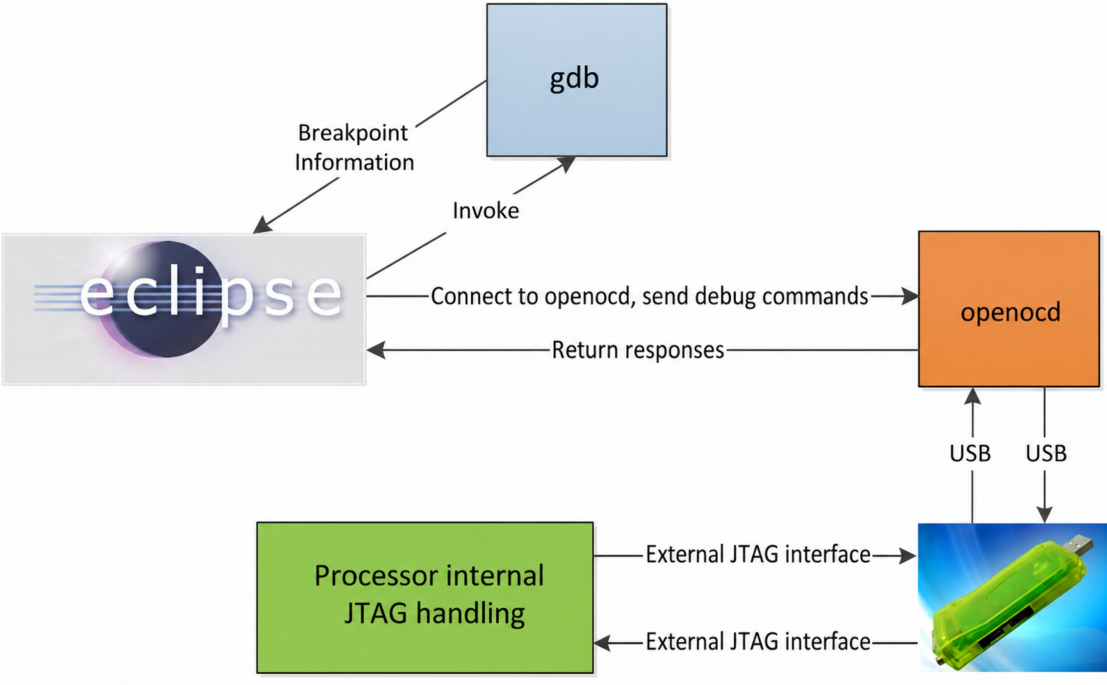
Quick Start
If this is your first time using JTAG for debugging, you can quickly run the entire process by following these steps:
-
Confirm hardware connection — Connect the TDI, TCK, TMS, and TDO of the JTAG debugger to the corresponding pins on the board. After the board is powered on, the JTAG tool should only turn on with a blue light. For details, please refer to the section Hardware connection and driver installation.
-
Install driver — Make sure the JTAG driver is installed (
BDT/ice/libusb-AICE-driver/Install_driver.exe). For details, please refer to the section Hardware connection and driver installation. -
Add pin enable in code — after the
gpio_init()call, addjtag_set_pin_en()(four-line JTAG) orsdp_set_pin_en()(two-line SDP) depending on the pattern. For details, please refer to the section Software and IDE configuration. -
Start ICEman — execute the four lines
./ICEman -Z v5, and the two-lineexecute ./ICEman -Z v5 -I aice_sdp.cfg, and record the output TCP port number (usually 1111). For details, please refer to the chapteron software and IDE configuration . -
Configure IDE Debug — Create a new C/C++ Remote Application, select the ELF file, set GDB to
riscv32-elf-gdb, and enter the port number output by ICEman for TCP ports. For details, please refer to the section IDE Debug configuration. -
Start Debugging — Click the Debug button, set breakpoints, and use features like Step Over / Resume to debug. For details, please refer to the section Breakpoints and Single-step debugging.
Tip
If you encounter problems along the way, please refer to the FAQ section for solutions.
Quick Connection Guide
Hardware connection and driver installation
-
Board wiring
After receiving the board, find the corresponding schematic and use the switch to switch between two-wire/four-wire modes. In principle, it automatically detects the default level of PB0 (which varies by chip; please refer to the schematic) upon power-on. GND is detected as four-wire, and 3v3 as two-wire.
Connect the JTAG debugger's TDI, TCK (clock source hclk), TMS, and TDO to the corresponding pins on the board. After connecting the signal cables, power on the chip. You can use the small black box 3v3 to connect to the board VBAT, or, if you have a USB module, use 5V to connect to VBUS. The chip outputs a voltage to the JTAG as a reference level, connects the board's 3V3 output voltage to the JTAG box REF, and provides the JTAG signal. TCK/TMS/TDI/TDO should operate at 3.3V to avoid damaging the IO or causing JTAG communication failure.
If the JTAG tool only lights up blue at this time, it indicates the wiring is normal; If a red light appears, it indicates a power supply issue or incorrect signal cable connections. You need to check the wiring and power supply.
-
JTAG driver installation
BDT/ice/libusb-AICE-driver/Install_driver.exe
When installing the IDE, this driver will be installed by default. If not installed, a red light may appear, so be sure to install this driver before use.
Software and IDE configuration
-
JTAG pin initialization
During program initialization,
gpio_shutdown(GPIO_ALL)/gpio_init()is called, and this interface will configure JTAG IO to GPIO mode, causing the JTAG connection to fail. Therefore, after initialization, you need to re-enable the JTAG pins:- Four-wire mode: Call
jtag_set_pin_en()to initialize the JTAG pins; - Two-wire mode: Call
sdp_set_pin_en()to initialize the SDP pins.
- Four-wire mode: Call
Note
If the above interfaces are not called, the JTAG debugger will not be able to connect properly to the target chip.
-
Connection command
Start ICEman, four-line mode executes:
./ICEman -Z v5, two-line mode executes:./ICEman -Z v5 -I aice_sdp.cfg
The ICEman tool (based on OpenOCD) has been successfully initialized and shows it is ready for use. Listing information such as the listening port, JTAG frequency, and target core indicates that communication between ICEman and the AICE-MINI+ debugger has been established and that ICEman has identified the target device (at least from the perspective of the JTAG interface). 1111 is the required TCP port number. During debugging, you need to ensure ICEman is running and the terminal cannot be closed.
ICEman is located in the
$IoTStudio/RDS/V5.1.1/ice/directory, and you can also open ICEman yourself.
Special connection instructions
For chips that support 32k_watchdog periodic reset (cyclic reset), the 32k_watchdog must be turned off when connecting JTAG; otherwise, the reset will clear the command written to the RAM (ICEman itself does not write instructions when connected; only memory can be written when executed), causing the JTAG connection to be disconnected again.
The steps to disable the 32k_watchdog are as follows:
- Download the latest Telink IoT Studio installer; extracting it will reveal the following contents:
Run TelinkIoTStudio_V2025.2.exe to install. After installation, you must run TelinkIoTStudio Updater.exe to update the components in IoT Studio to the latest version.
Make sure that after the update, to use the JTAG feature, open the ICEman terminal in IoT Studio (after startup, other operations are the same as on other chips):
Executing in the shell:
./start_ICEman.sh
You can launch ICEman.
JTAG burning
There are two JTAG burning methods: Telink IoT Studio IDE and Andes IDE.
(1) Telink IoT Studio IDE
The interface is as follows:
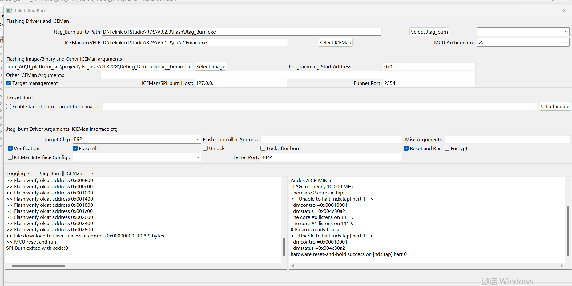
(2) Andes IDE
The interface is as follows:
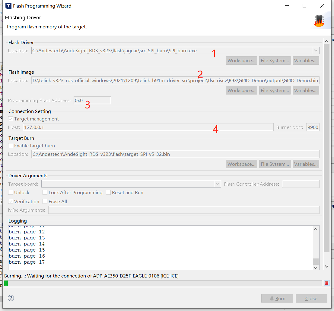 for flash programming with JTAG
-
1 is the software download path;
-
2 is the BIN file to be downloaded;
-
3 is the offset address for Flash;
-
4 is the address and port number to connect to during download. If you fill in the wrong box or fail to check the box, the download code will be incorrect.
Note
When programming Flash via JTAG, first confirm the JTAG connection is correct. If unsuccessful, try setting the target to ICE and checking SDP (dual wire).
Debugging of the D25
IDE Debugging configuration
- After ICEman starts, click the
Debugicon on the toolbar and pull down the arrow to selectDebug Configuration.
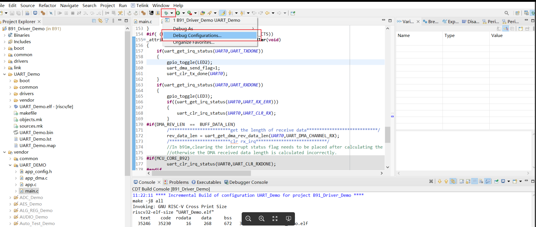
- Select C/C++ Remote Application, configure the
Maintab, choose the compiled .elf file as input for gdb, and chooseDisable auto build.
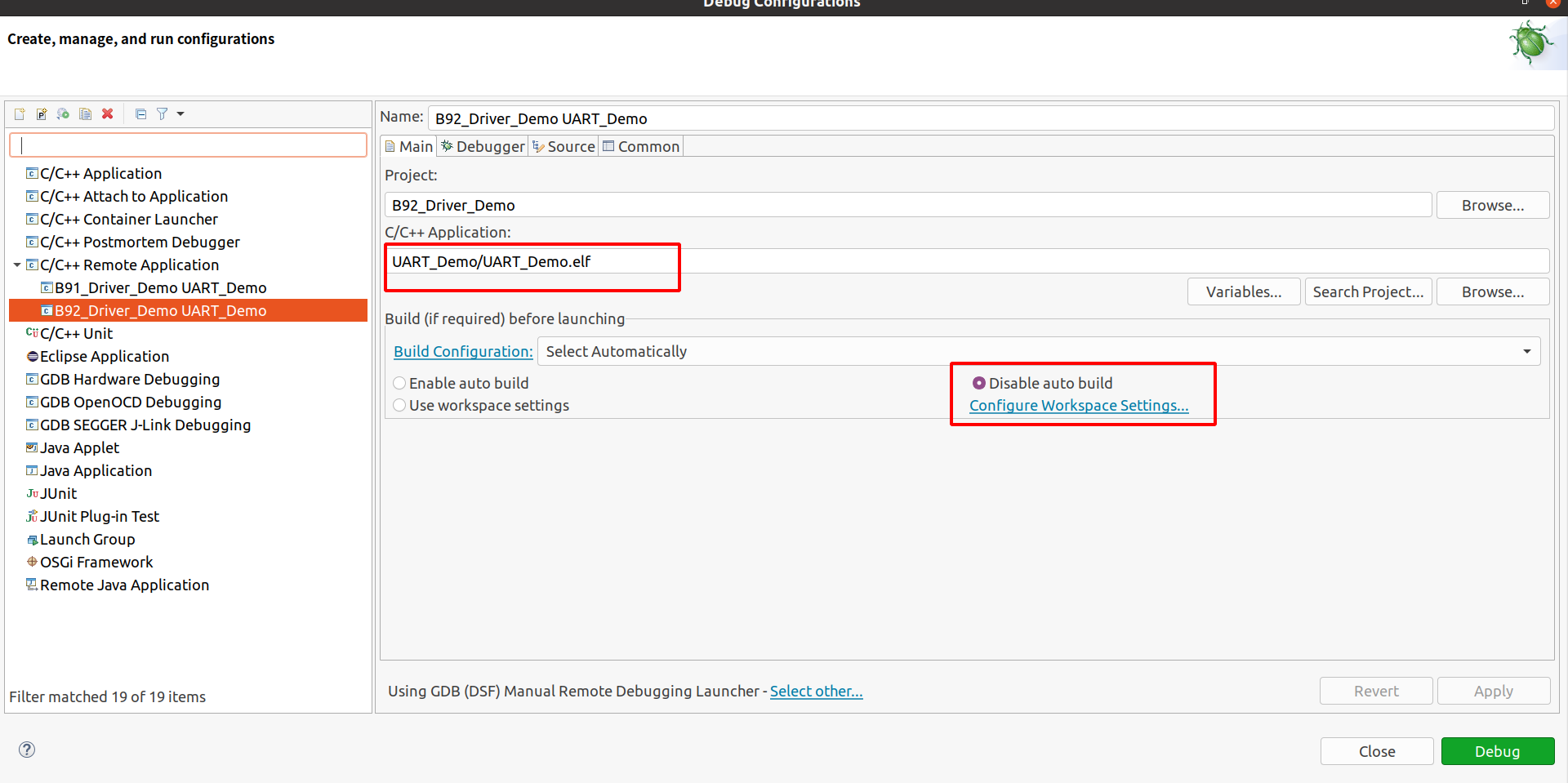
- Click
Select otherat the bottom and chooseManual(default isAutomatic).
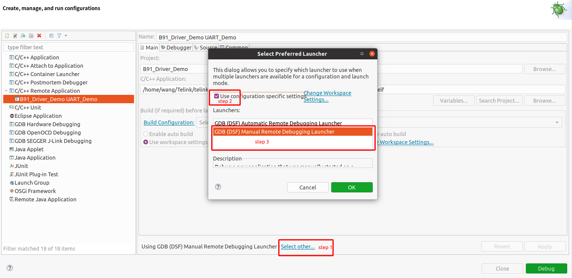
- Click the
Debuggertab and configure the corresponding debugger. This isriscv32-elf-gdb. Be careful not to check Stop on startup at.
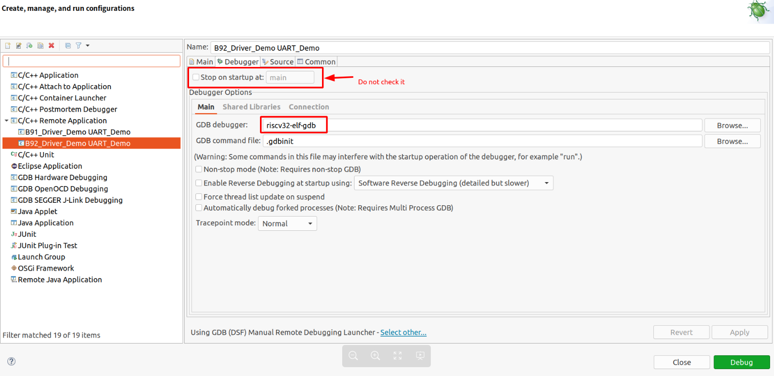
- Click the
Connectsubtab and enter theTCPport number as the1111obtained by ICEman.
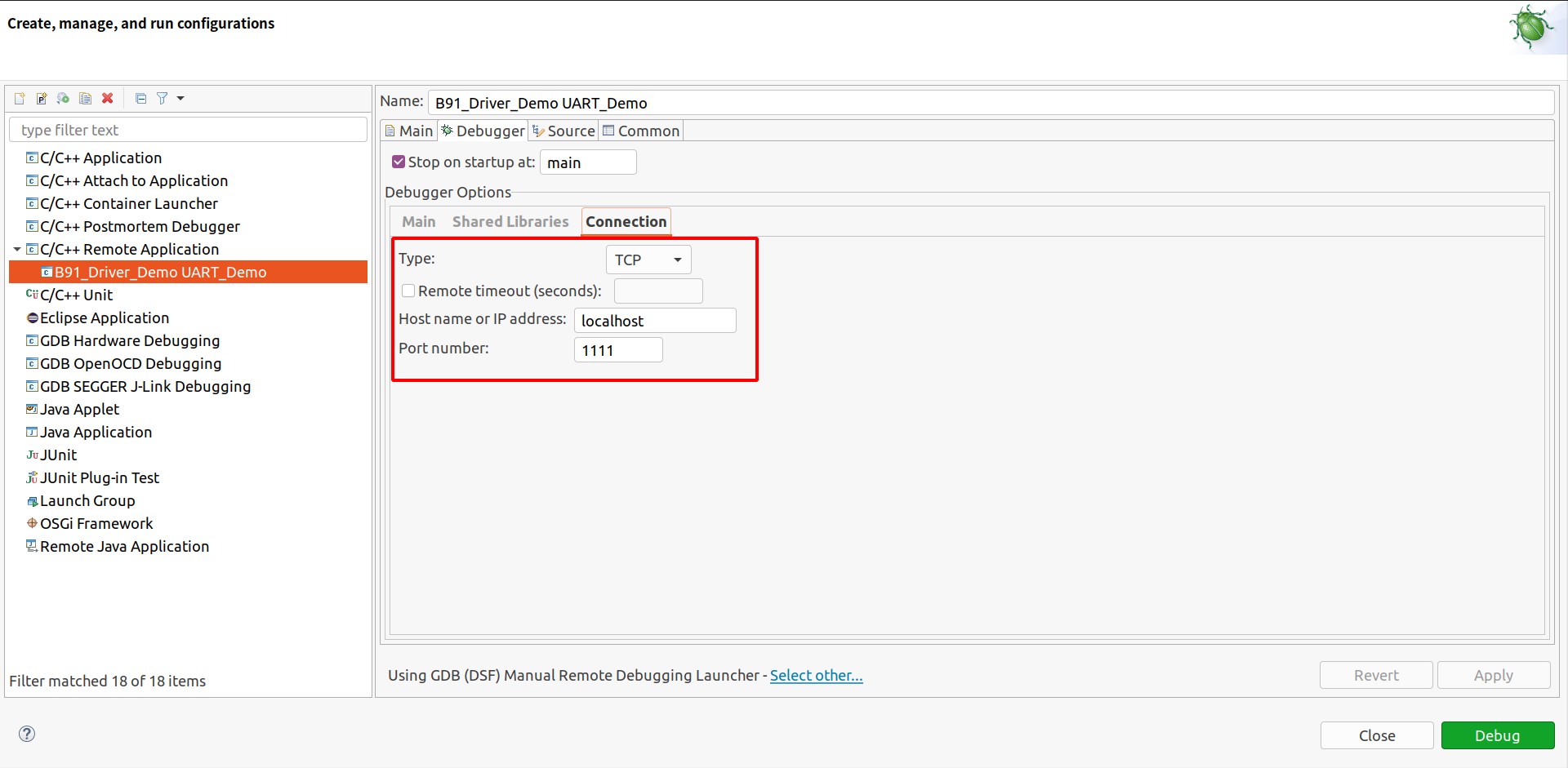
- Once configuration is complete, click the
Debugbutton and add breakpoints to start debugging.
In the Startup interface, the Set breakpoint at option can set the position of the first breakpoint during startup debugging. You can set it to main, meaning that after debugging starts, it will default to the main function entry. After completing the above configuration, click the Debug button in the lower right corner to start debugging. Next time you debug, this configuration will appear under your name under the debug button. Just click it to restart debugging.
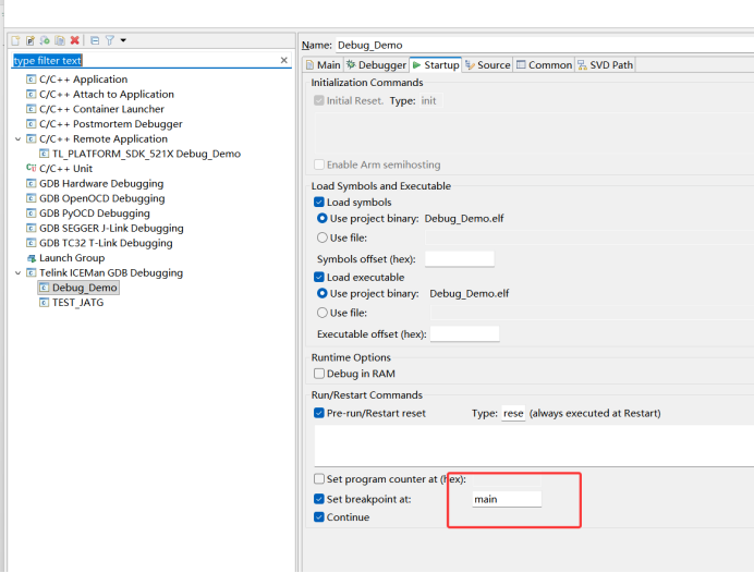
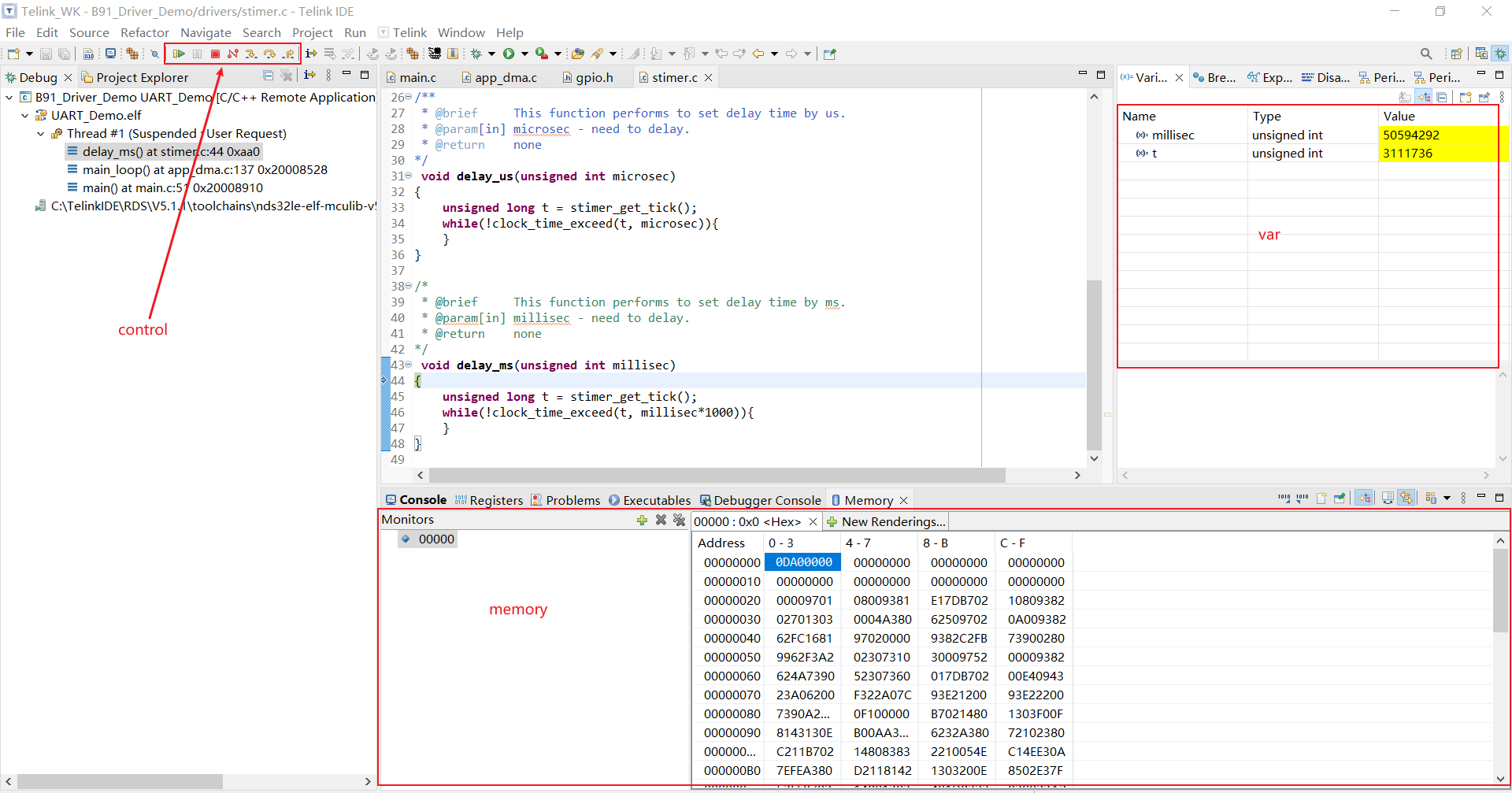
Breakpoint
Currently, TLSR9 series SoCs support up to two hardware breakpoints. When you find that your program's starting address is 0x20000000, it means it is running inside flash and requires hardware breakpoints. Commands like step in or step over use a breakpoint so that users can define only one breakpoint during debugging; otherwise, exceptions will occur. This is also why it's not recommended to check Stop on startup at, because this option actually sets a breakpoint.
If you encounter a CANNOT ACCESS MEMORY AT ADDRESS XX exception during debugging, you can use the info br command to check the number of breakpoints.
After entering debug mode, double-click the left side of the row number where the program needs to stop to set a breakpoint. The breakpoint status is as follows:

Note
-
A checkmark must be present before the breakpoint; otherwise, the breakpoint is invalid.
-
The program stop position may be one or two lines after setting the breakpoint (this is normal).
Click the Resume button to execute the program to the breakpoint; click again to proceed to the next breakpoint.
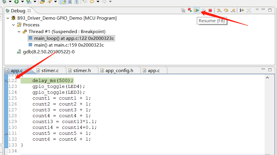
Link to source files
During breakpoint debugging, an error may occur where the source file cannot be found. At this point, click Edit Source Path..., as shown below:
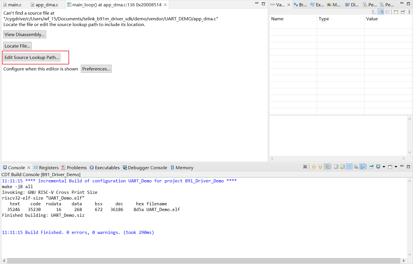
Click Add, select Path Mapping, and edit as follows:
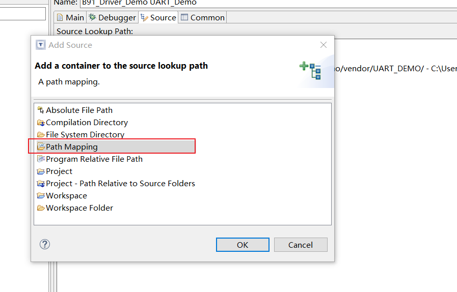
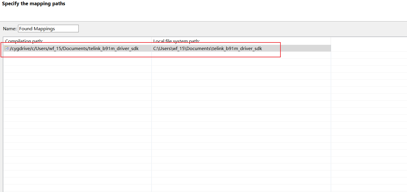
The left side requires manual input, while the right side selects the path.
The principle is to correctly map the path in IoT Studio to the local path; the simplest approach is to map /cygdrive/c/ to C:\ (since the SDK is on the C drive).
Once the above configuration is complete, normal debugging can proceed.
Single-step debugging
-
Step Into: Single-step debugging triggers execution of a subfunction when encountering it
-
Step Over: Single-step debugging that does not execute a child function when encountering it
Note
If an error occurs during Step Into debugging (due to database closure or other reasons), it is recommended to use Step Over or breakpoint methods instead.
Introduction to the debugging toolbar and interface
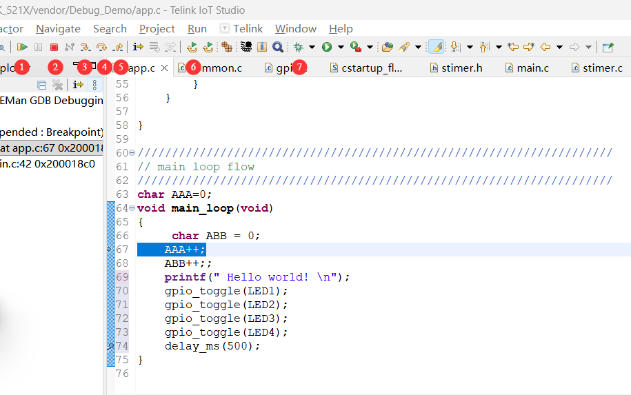
The functions of the debugging toolbar are as follows:
(1) Resume: After the breakpoint pauses, the program continues at full speed from here until the next breakpoint or manual pause;
(2) Terminate: Ends the current JTAG/GDB debugging session;
(3) Step Into: Jump in in one step;
(4) Step Over: Skip in a single step, run the entire line without entering the subfunction, skip directly to the next line;
(5) Step Return: Step out, execute the remaining code from the current function in one go, then return to the upper-level call;
(6) Restart: Restarting debugging;
(7) Debug: Enable debugging or enable related debugging configurations.
In the Windows above the IDE, click Show View to see debugging-related tabs, the most commonly used being
Memory: View values in memory;Expressions: Parse variables or variable expressions;Registers: View registers on the kernel.
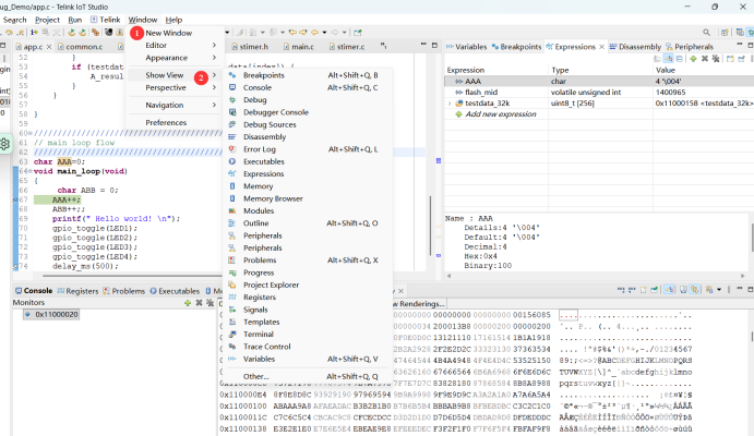
Multi-core debugging
N22 debugging
-
Connection
No need to select N22 or D25F; select the toolchain. D25F uses v5f for engineering and v5 for N22 projects; the compiler doesn't need to know which core it is. For JTAG connections, if both cores are running normally, OpenOCD will create two socket ports, and the host computer controls the two cores through these ports.
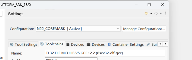
-
Differences between N22 and D25F tuning
a. Before debugging N22, the N22 must be able to run normally. N22 and DSP are reset by default and need to be awakened via mailbox in the D25F code before N22 can take instructions from flash 0x80000 and run them (see description in c below).
b. When debugging N22 using IDE breakpoints, configure as shown in the diagram below. The default
Core_Configurationoption iscore0, but changing it tocore1can also work normally.Note
- Do not check 'Reset_and_Hold' in the 'Startup' option. If checked, N22 will reset, and there will be no external action to open N22, causing debugging errors
- The default option for 'Program' under the 'Main' checkbox in the image below may be incorrect and needs to be fixed.
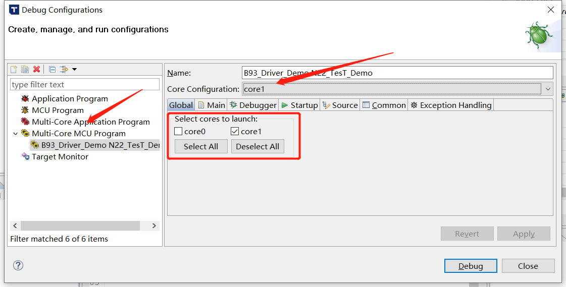
c. The D25F code is at flash 0, the N22 code at flash 0x80000, and the DSP code at flash 0x40000. A mailbox is added between the three cores, similar to how software interrupts work. D25F writes data to this address, then generates an interrupt and sends it to N22, which reads this address and receives the information. D25F is the main controller. N22 and DSP are reset by default. When D25F is ready, open N22 and DSP, and only then will N22 and DSP fetch instructions from Flash to run. Telnet debugging is the same as with the D25F, but attention must be paid to memory address allocation when reading or writing memory.
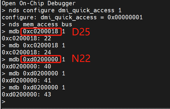
-
N22 and D25F joint debugging
Method: First, debug one core in the IDE as described above, then continue debugging the other core. In the Debug selection, select the corresponding core to operate. The operation method is the same as single-core debugging. The Kanban board can only view data from the current debug core.
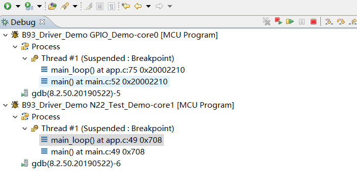
DSP debugging
- Configure the environment
Note
32-bit systems were not tested; according to xtensa_debug_guide.pdf, XOCD (software to be installed below) is only compatible with 64-bit systems. Additionally, the following only covers installation on Windows; for Linux, please refer to the relevant manuals and the steps below.
Step 1: Close the antivirus software and install "Xplorer-9.0.17-windows-installer.exe" as administrator. The installation path should be the default setting; opening it for the first time will cause errors (if no error occurs, you must follow the solution). The solution is: right-click on Properties in the software shortcut, add --xxtrace (with a space before --) in the target (T) input box, select "Install Software Keys" in the license detection popup, and enter 27001@192.168.51.135. Then close the software and remove --xxtrace, after which the IDE can work normally.
Step 2: Install "xt-ocd-14.07-windows64-installer.exe" according to Section 7.3 of "xtensa_debug_guide.pdf". Both the documentation and installation package are located in the software installation directory in Step 1.
Step 3: Install J-Link probe support according to chapter 7.3.2 of "xtensa_debug_guide.pdf". Here, you will install version V7.56 downloaded from the official segger website.
Step 4: Modify the file topology.xml in the XOCD installation path from Step 2. The usbser value is the SN number of the JLink, which can be viewed through in the SEGGER J-Link Configuration software (JLinkConfig.exe at the JLink installation path). When modifying and saving files, make sure the file encoding remains unchanged. It's best to use software like "XML Editor" to modify it.
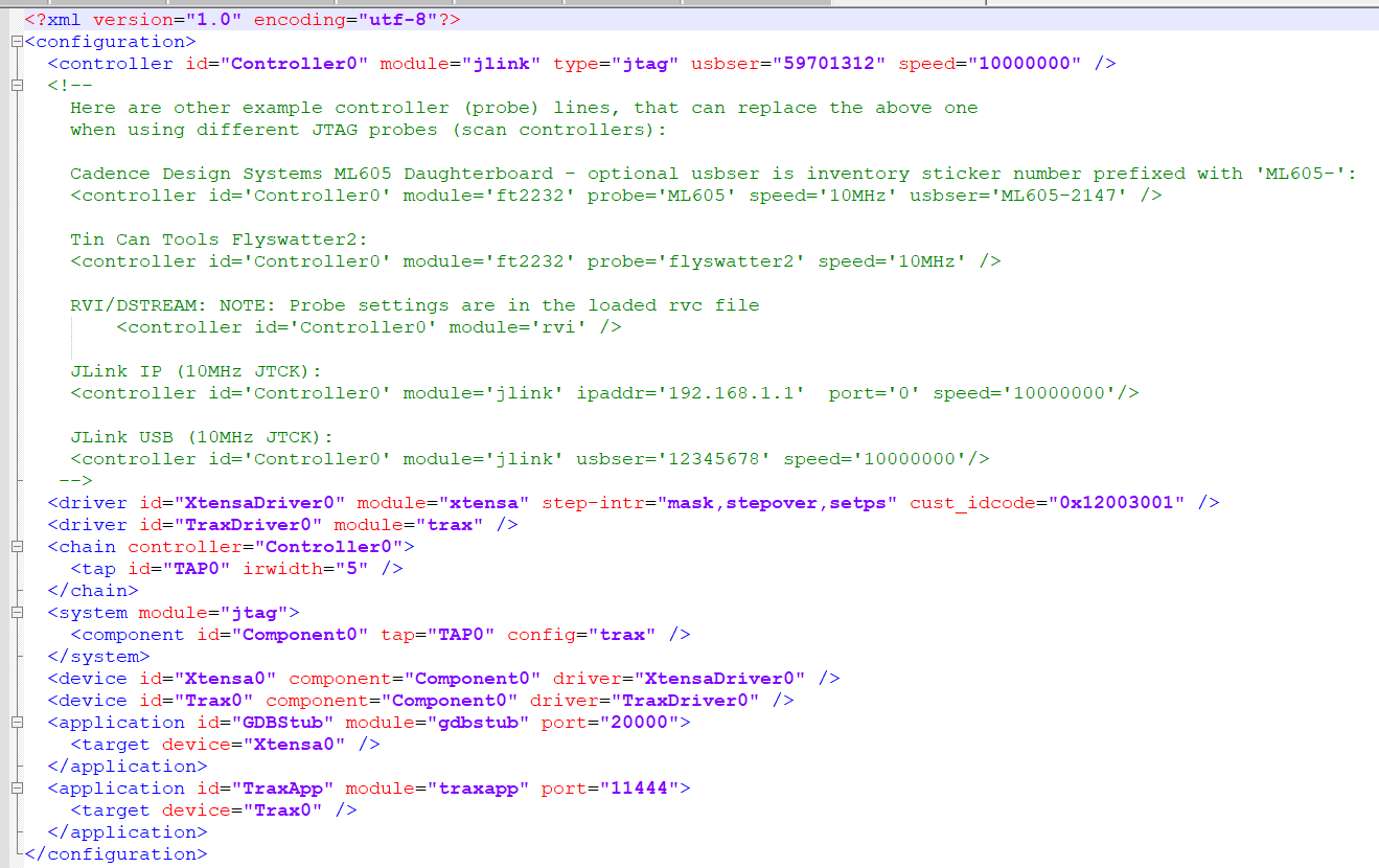
- Import and compile the project
Step 1: Open the IDE and create a new workspace. Copy the boot_1028.xws from the \PCDB\prj\Onca\tst\dsp folder into the workspace.
Step 2: Delete the HelloWorld project. In the project navigation panel, right-click and select "Import" -> "Import Xtensa Xplorer Workspace", choose boot_1028.xws, Click Next, and select everything at every step (if the option is marked in red, it means it was previously selected. You don't need to select it now, but continue next).
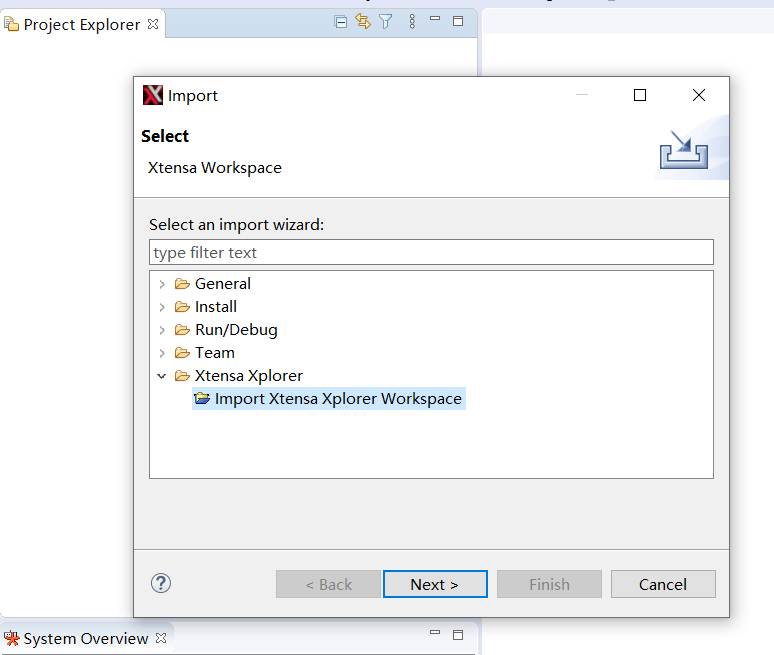
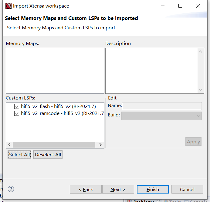
Step 3: You can create a new project as prompted. Here, it demonstrates directly importing an existing project. Here, copy the dsp_led folder from \PCDB\prj\Onca\fw\boot\dsp_rw to the workspace, right-click "Import" in the project navigation panel, select "Import" -> "Existing Projects into Workspace", then select the dsp_led folder to import the project.
Step 4: Configure as follows, click the compile button, and after successful compilation, "Build successful!!" will be printed on the console.


Step 5: Follow the prompts to find the object file dsp_led and copy dsp_led to the C:\usr\xtensa\XtDevTools\install\tools\RI-2021.7-win32\XtensaTools\bin directory.
Step 6: Add XTENSA_CORE to the Windows environment variable with a value of hifi5_v2. Open cmd at C:\usr\xtensa\XtDevTools\install\tools\RI-2021.7-win32\XtensaTools\bin and execute:
xt-objcopy.exe –O binary –S dsp_led dsp_led.bin
xt-objdump.exe -D dsp_led > assemble.txt
Solution 2: Right-click the project and click "Open Command Shell", then refer to the readme.txt under \PCDB\prj\Onca\tst\dsp.
Step 7: If no link file is specified during compilation, you need to add a link file (default is a SIM file, which needs to be modified).
Open the IDE, create a new workspace, and copy boot_1028.xws from the \PCDB\prj\Onca\tst\dsp folder into the workspace (if you ran it before, you don't need to do it again). This step is to facilitate the provision of the link files needed for future projects. If you have special requirements for optimization options or other options, you can configure them in this interface.
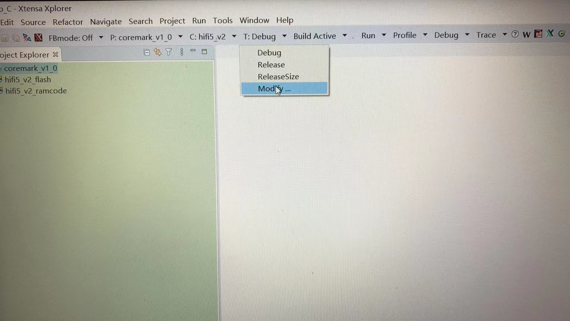
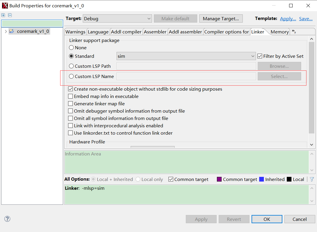
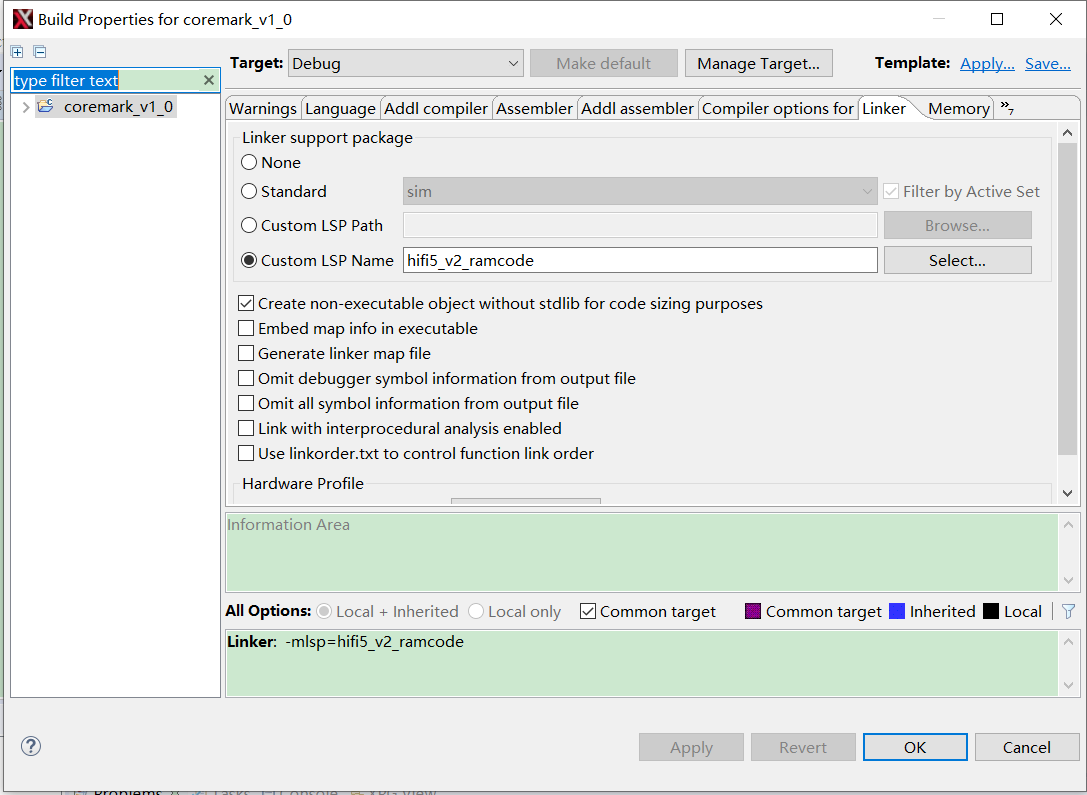
- Other preparations before commissioning
Step 1: Download the bin file generated above to the Flash address 0x40000.
Step 2: Set PB4 - PB7 to JTAG multiplexing and use D25F to enable the DSP core. Here, this is done by opening wpcdb, executing the d25f_enable_dsp script, and then resetting the chip. By observing experimental phenomena, one can determine whether the program is executed correctly.
After JTAG RST, continue debugging the function
./ICEman -Z v5 -H
After executing this command, the program resets the digital registers but not the analog registers. You can see the program remains at the entry point, while the JTAG remains connected.
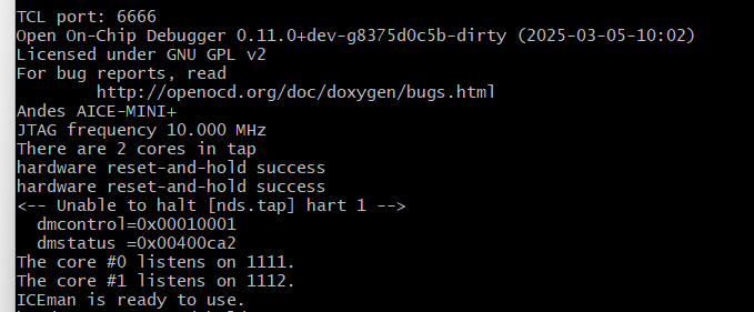
View and modify registers and memory through tabs
Expressions tab
In the Expressions tab, you can view variables and variable expressions, and directly modify the corresponding value in the Value section.
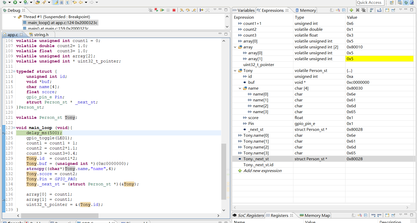
Memory tab
View/modify memory data in the Memory tab.
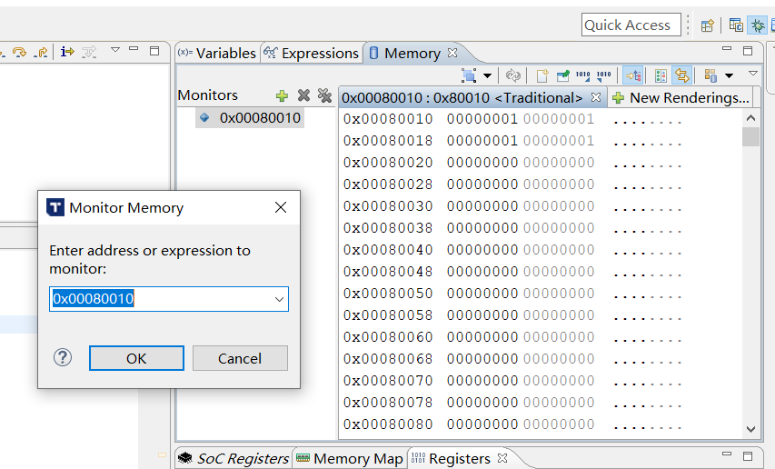
Click the magnifying glass icon in the upper right corner, and the Monitor Memory dialog box will pop up as follows:
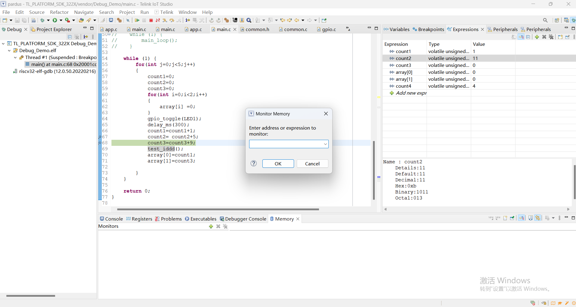
Registers tab
View/modify CPU register data in the Registers tab.
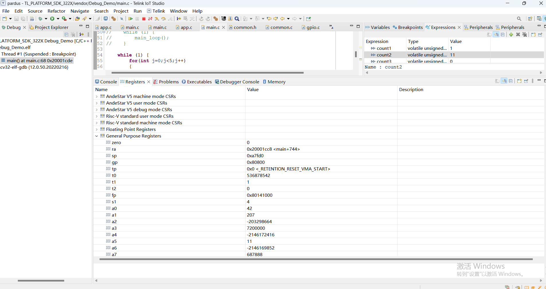
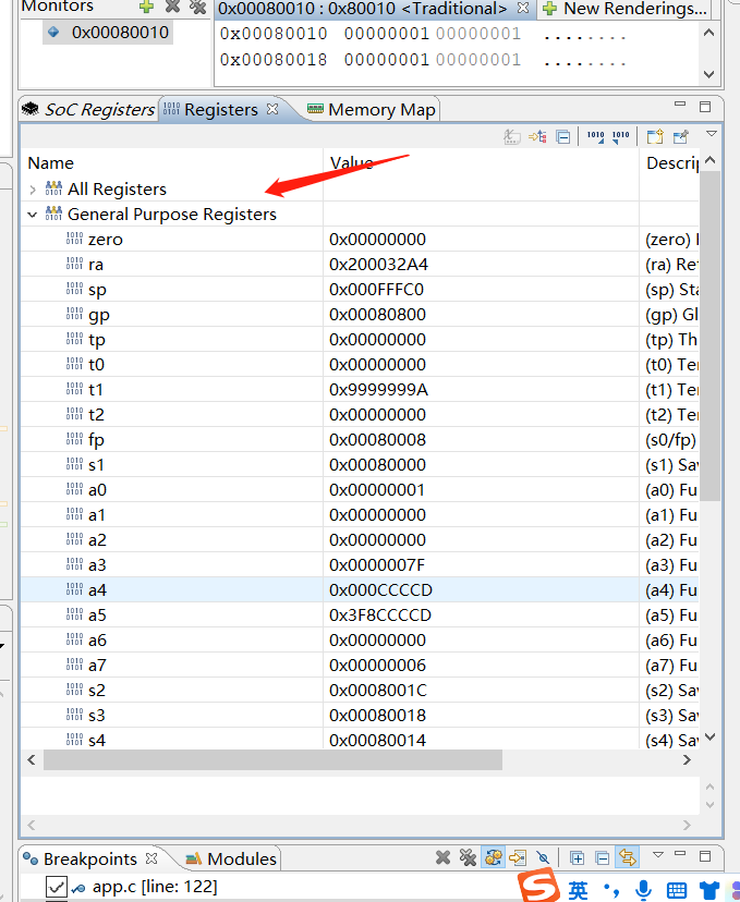
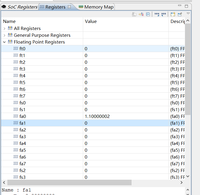
GDB common commands usage
Enter the corresponding command in the red box shown below to perform read/write operations on registers/memory.
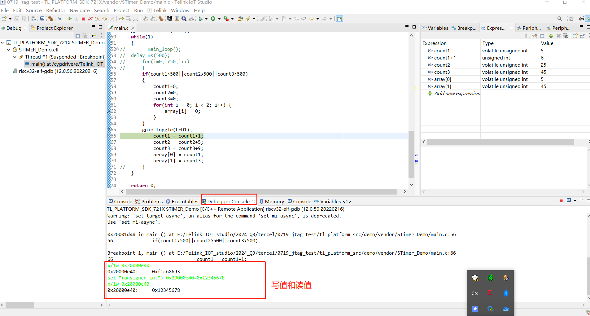
An example of the verification process is as follows:
x/1w 0x20000e40
0x20000e40 <main+452>: 0x00f92223
x/1w 0x80140204
0x80140204: 0x0e0fffff
set *(unsigned int*) 0x80140204=0x0e0f55aa
x/1w 0x80140204
0x80140204: 0x0e0f55aa
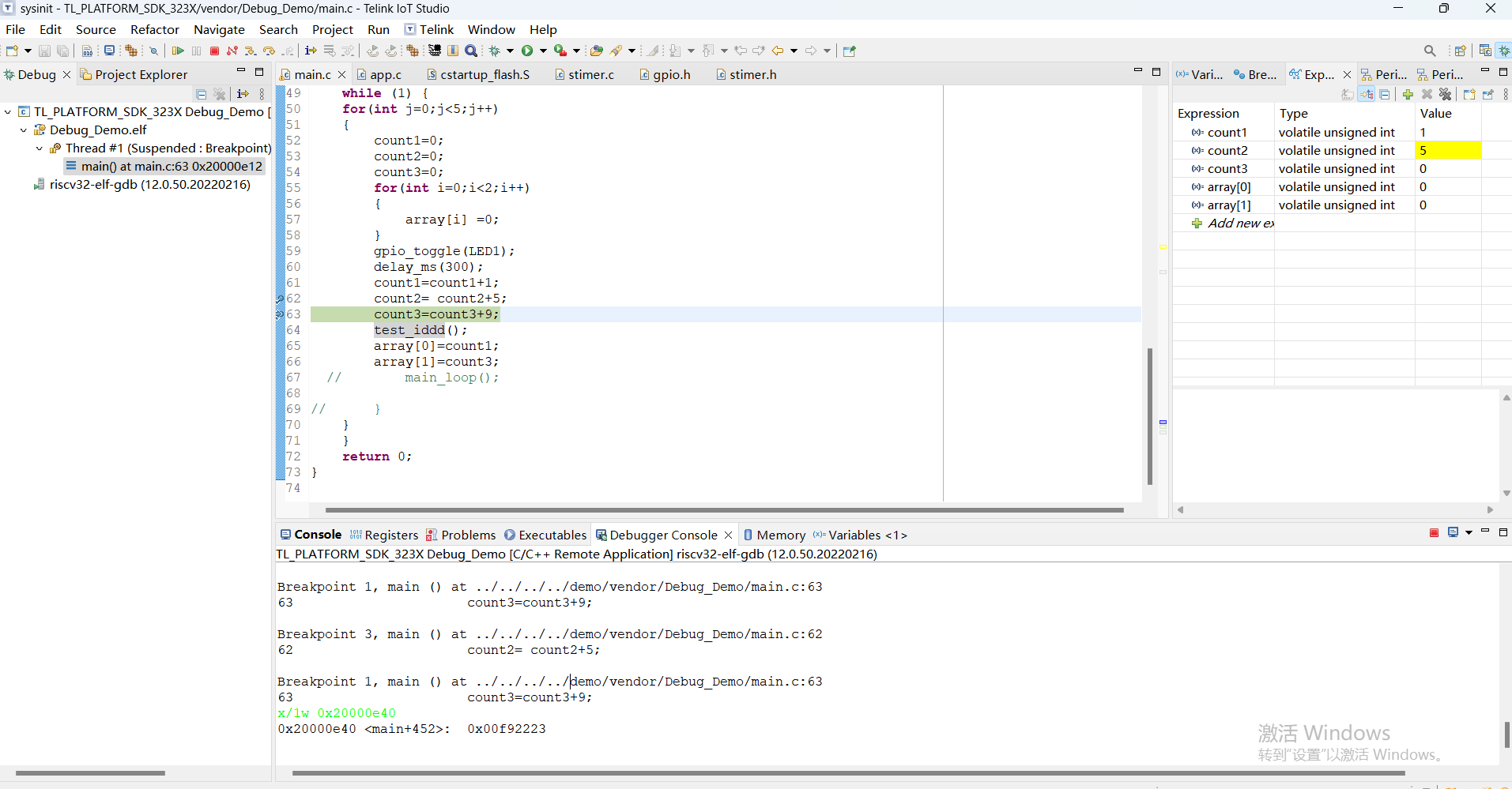
Read the command
| Command | Description |
|---|---|
x/1w 0x80170000 |
Read a Word data from the 0x80170000 |
x/1h 0x80170000 |
Read half-word data from the 0x80170000 |
x/1b 0x80170000 |
Read a byte's data from the 0x80170000 |
Among them:
x/: indicates read1: Read the quantityw: Unit (word)
Write instructions
| Command | Description |
|---|---|
set *(unsigned int*) 0x80140420=0x12345678 |
Write a word 0x80140420 address with a value of 0x12345678 |
set *(unsigned short*) 0x80140420=0x12345678 |
Write half word 0x80140420 address, with a value of 0x5678 |
set *(unsigned char*) 0x80140420=0x12345678 |
Write 1 byte 0x80140420 address with a value of 0x78 |
Among them:
set: represents writingunsigned char: writes to the units0x80140420: Write the address0x12345678: Write the value
Note
Some test instructions do not support this, such as 'tui enable'.
Use JTAG on VS Code
For detailed instructions on debugging using JTAG in VS Code, please refer to the official Telink documentation:
Telink VS Code Extension User Guide
Debugging with Segger
Segger J-Link is a mainstream debugger that supports JTAG and SWD interfaces and is suitable for program downloads, online debugging, and Flash programming. This chapter introduces the basic usage of the Segger J-Link tool on Telink chips. For users, this is equivalent to having two sets of host computers and debuggers. Telink JTAG Black Box Debugger and Segger Debugger can both be used, with the same functions.
J-Link driver installation
Download the J-Link driver installation package from the Segger official website: https://www.segger.com/downloads/jlink/
After installation, connect the J-Link debugger to your PC via USB, and the device manager will recognize it.
Used by J-Link Commander
J-Link Commander is a command-line tool built into J-Link that can be used to perform operations such as connect target chips, read and write memory and registers.
Open J-Link Commander and enter the following command to connect to the target chip:
connect
Select the target device (RISC-V core, selected according to the actual chip model) as prompted, choose the interface (JTAG or SWD), and select the speed (4000kHz or auto is recommended).
After a successful connection, you can use the following commonly used commands:
| Command | Description |
|---|---|
r |
Reset the target chip |
g |
Begin the execution procedure |
h |
Stop the execution of the procedure |
mem32 <addr> <count> |
Read 32-bit memory |
w4 <addr> <value> |
Write 32-bit memory |
reg |
View all registers |
reg <regname> <value> |
Write to the specified register |
loadfile <filepath> <addr> |
Download the file to the specified address |
erase |
Erase Flash |
exit |
Exit J-Link Commander |
J-Flash Usage
J-Flash is a flash programming tool from Segger that supports programming of target chips via J-Link.
Step 1: Open J-Flash, create a new project, or open an existing project.
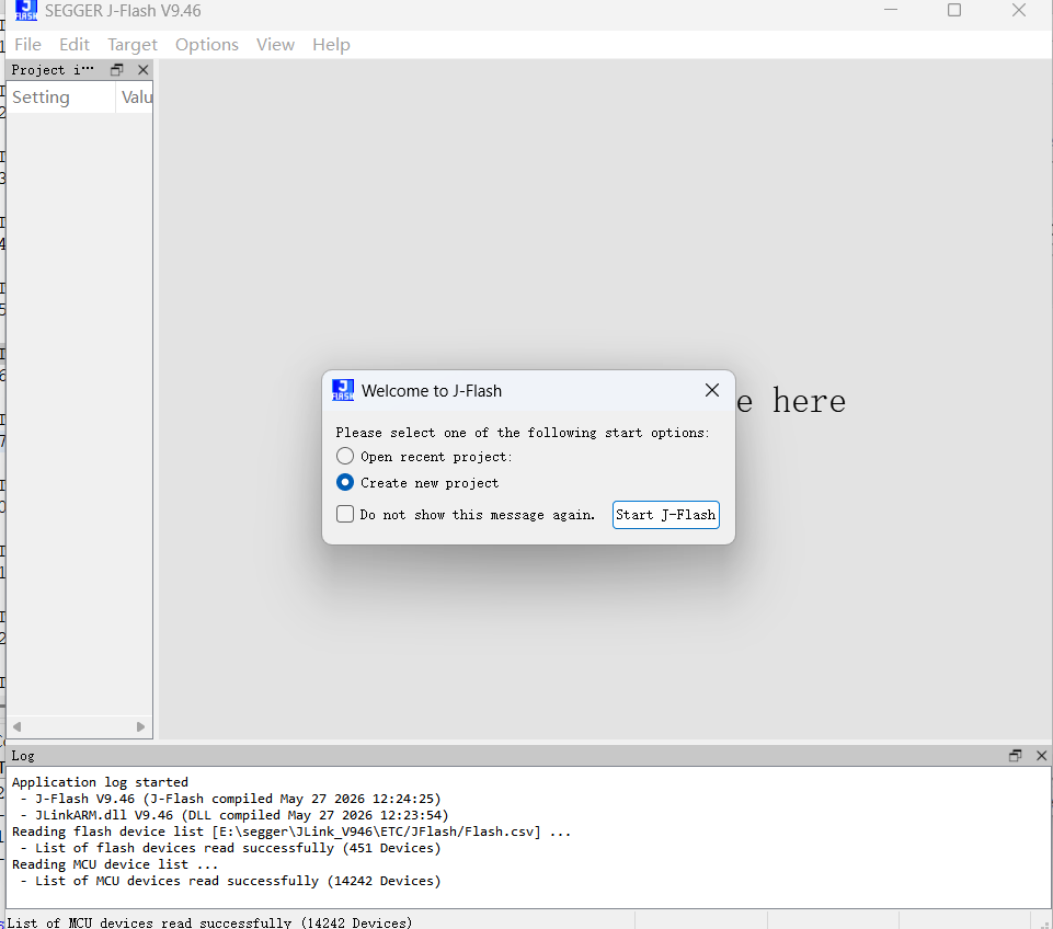
Step 2: Configure the target chip model, interface type (JTAG/SWD), and connection speed.
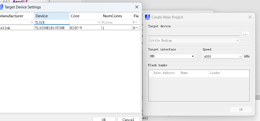
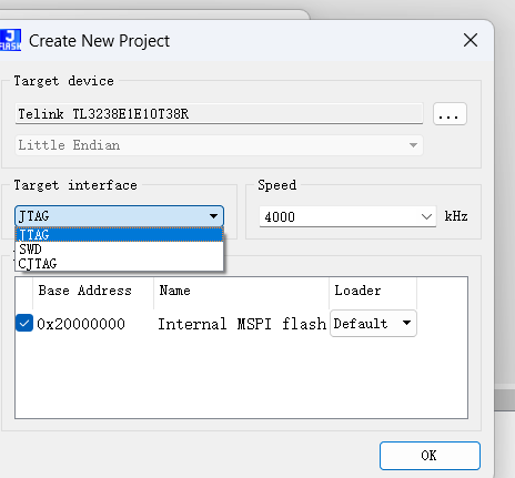
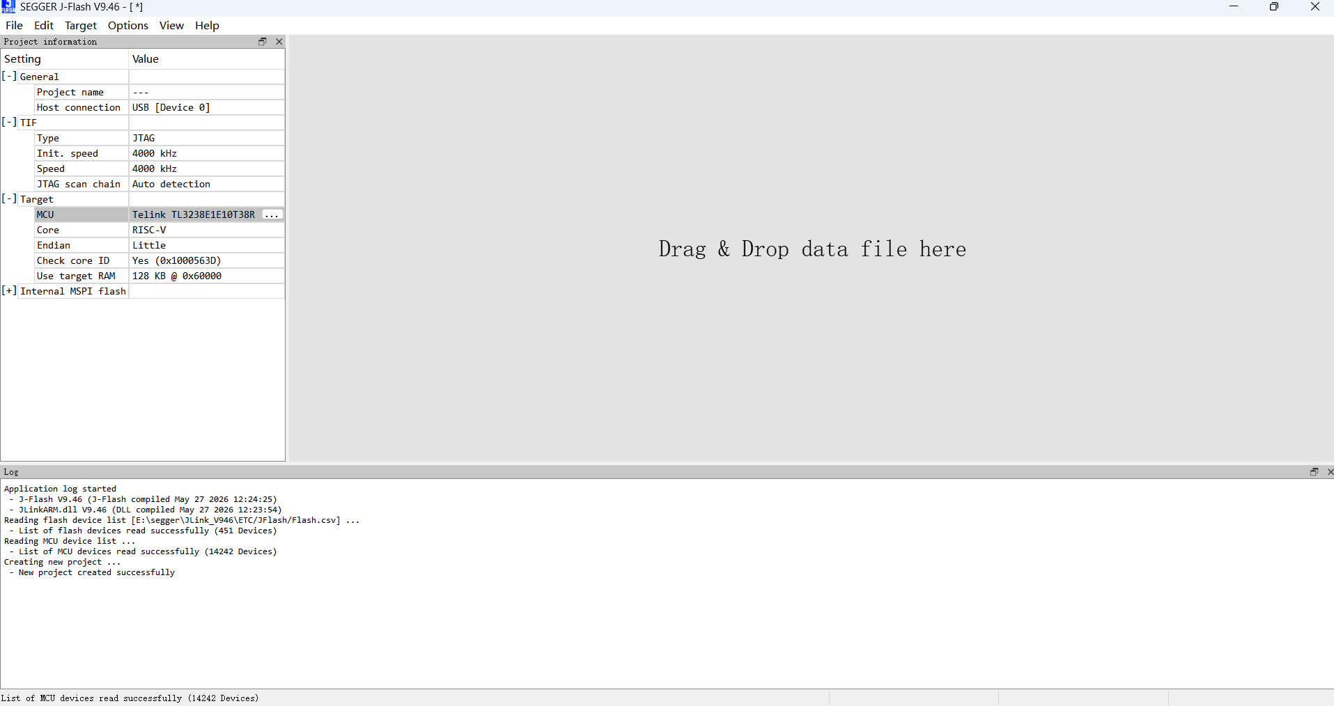

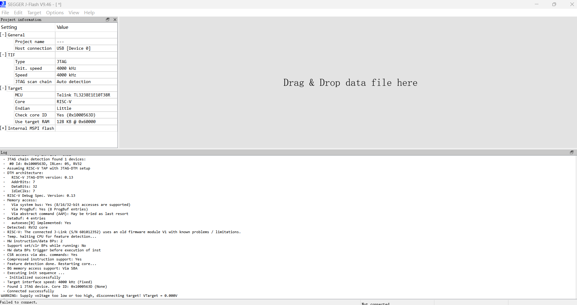
Step 3: Open the HEX or BIN file you want to burn.
Step 4: Click the "Program Device" button to burn, or use the shortcut key F7.
J-Link GDB Server Usage
J-Link GDB Server can use J-Link as a GDB debugging server, cooperating with GDB clients for online debugging. The following example uses multi-core chips.
- Install the JLINK package
Before debugging with JLINK, you need to download the JLINK suite from the Segger official website, including the JLINK driver and host program. After testing, it is recommended to install the more stable version V7.96f:
https://www.segger.cn/downloads/jlink/JLink_Windows_V796f_x86_64.exe
- Start the JLinkGDBServerCL.exe in the command line
Find the installed JLink folder, enter cmd in the file explorer's address bar, and press Enter:
In the opened CMD window, enter the command to start JLinkGDBServerCL.exe. To debug the D25F core, enter the following command:
JLinkGDBServerCL.exe -select USB -device rv32 -endian little -if JTAG -speed 1000 -noir -noreset -nogui -LocalhostOnly -nologtofile -port 2331
To debug the N22 core, enter the following command:
JLinkGDBServerCL.exe -select USB -device rv32 -endian little -if JTAG -speed 1000 -noir -noreset -nogui -LocalhostOnly -nologtofile -port 2331 -jtagconf 5,1
-port can be customized. If the connection succeeds, the following log will appear:
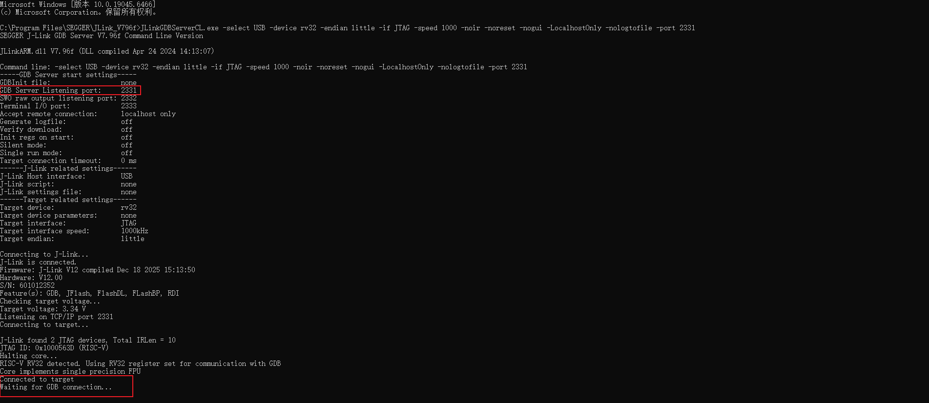
Note that the number GDB Server Listening port may differ from the -port you specified. The final GDB Server Listening port is based on the log.
- Configure JLINK debugging in IoT Studio
Step 1: Create a new C/C++ Remote Application
After compiling and downloading the program, as shown in the figure, click to select the program you want to debug (ELF file):
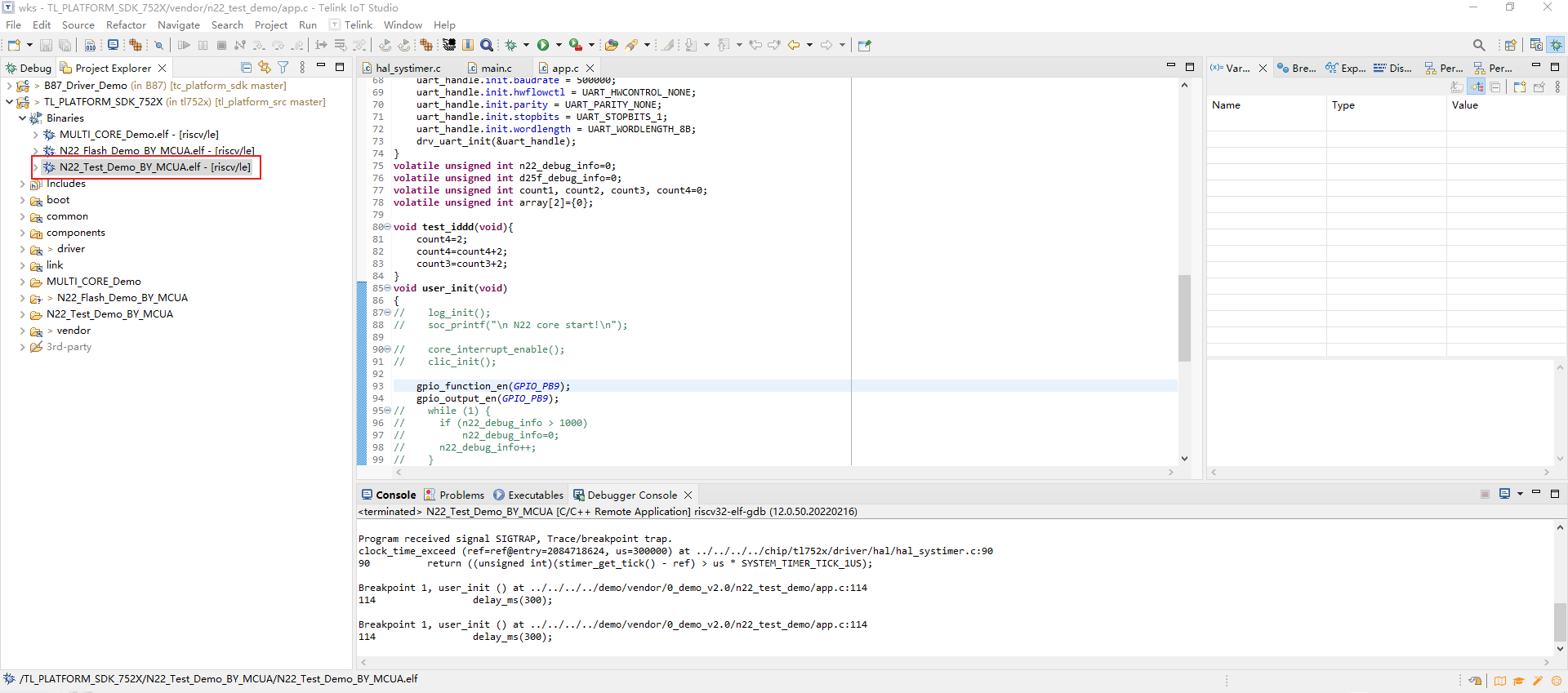 you want to debug
Then open Debug Configurations, double-click C/C++ Remote Application, and you'll see that the newly created Debug Configuration can automatically fill in the previously selected ELF file.
Step 2: Configure the Main tab
Click the Main tab to configure the following settings:
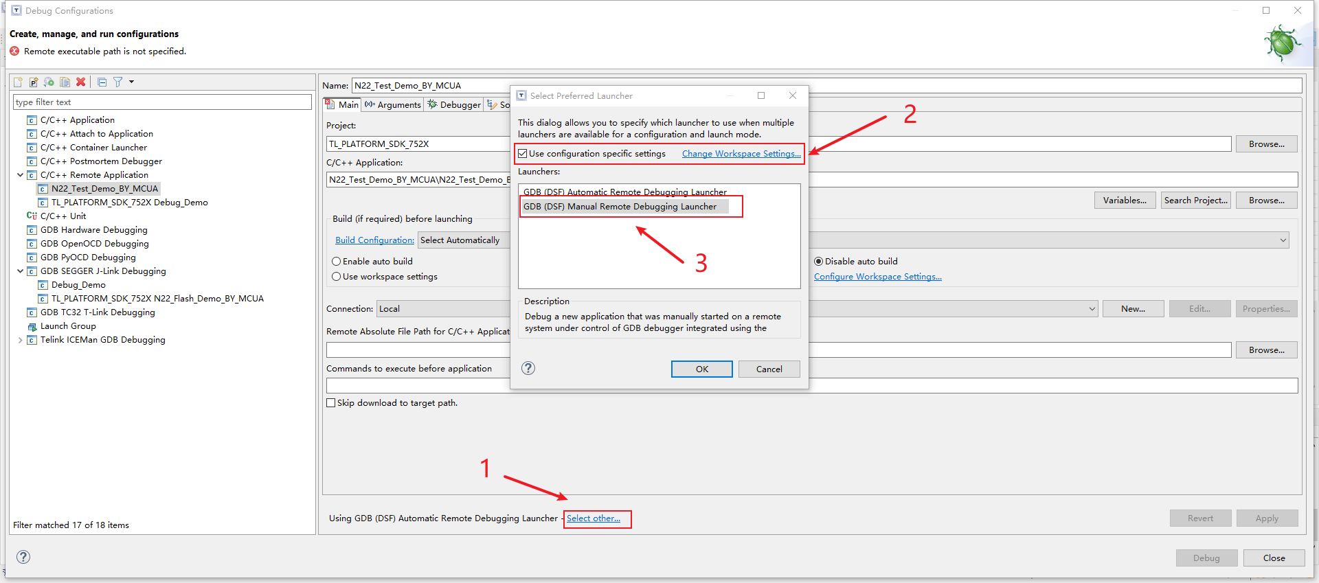
Step 3: Configure the Debugger option
Click the Main tab in the Debugger tab to make the following changes:
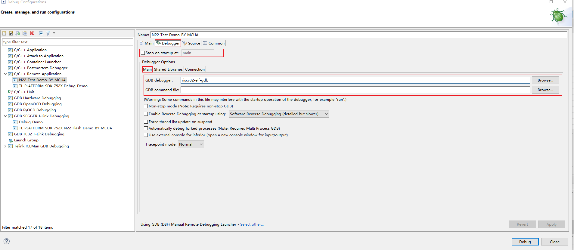
- Uncheck
Stop on startup at: - GDB Debugger: Change to
riscv32-elf-gdb - GDB command file: If there is no need to customize the gdb init command, leave it empty
Click the Connection tab and fill in the port number of the GDB Server Listening port you previously obtained:
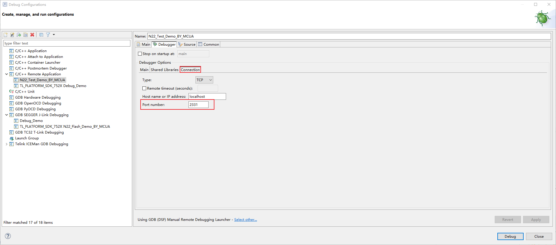
After completing the configuration, you can start debugging.
Note
Before using the Segger J-Link tool, please ensure that the JTAG pins are properly initialized (refer to the section Software and IDE Configuration for JTAG pin initialization) and that the hardware connection is normal.
FAQ
This section summarizes high-frequency issues and solutions during JTAG debugging. If you encounter any issues, you can look them up here.
Hardware connection
Q: What should I do if the JTAG debugging tool shows a red light?
A: Possible causes and troubleshooting steps:
-
Power supply abnormal — Check whether the board is powered on and whether the VBAT/VBUS voltage is normal. It is recommended to connect the blank chip first.
-
REF level not connected — Make sure the board's 3.3V output is connected to the REF pin of the JTAG box.
-
Signal line misconnection — Check each TDI, TCK, TMS, TDO to ensure they correspond to the board's schematic.
-
Driver not installed — Run
BDT/ice/libusb-AICE-driver/Install_driver.exeto install the driver.
Q: Wiring is normal (blue light on), but ICEman cannot recognize the chip?
A:
-
Check whether
the code calls jtag_set_pin_en()(four-wire) orsdp_set_pin_en()(two-wire). For details, please refer to the section software and IDE configuration. -
Find the schematic of the board and find the corresponding pins for JTAG_CTR. Generally, when connected to GND, this pin operates in four-wire mode; when connected to 3v3, it operates in two-wire mode.
-
Confirm that the two-wire/four-wire mode switch settings match the ICEman startup parameters.
-
After repowering on and resetting the chip, restart ICEman.
Connection and Communications
Q: Did ICEman disconnect quickly after connecting?
A: Commonly found in chips with a 32k_watchdog periodic reset (such as TL322x, TL323x), the reset clears the command ICEman uses to write RAM. You need to refer to the method in section Special connection instructions and launch ICEman with the latest version of IoT Studio to disable the 32k_watchdog.
Q: After starting ICEman, does it prompt that the port is already in use?
A: This indicates that the previous ICEman process did not exit properly. Run ./ICEman -Z v5 -k in the terminal to clear residual processes, then restart.
Breakpoints and debugging
Q: Breakpoints are set, but the program won't stop?
A:
-
Before checking breakpoints in IDE Debug mode, check for checkmarks; if not, breakpoints are not active.
-
The number of hardware breakpoints supported is limited. Use the
info brcommand to confirm whether the current breakpoint count has been reached. Additionally, Step Into/Step Over occupies a single breakpoint. For details, please refer to the section Breakpoints.
Q: Is there a CANNOT ACCESS MEMORY AT ADDRESS XX error during debugging?
A: This is usually caused by the number of breakpoints exceeding the limit. Enter info br in the GDB console to check the current number of breakpoints, delete any redundant ones, and then retry.
Q: Can't enter the Step Into function?
A: If the function is located in a prepackaged library (no source code), Step Into will fail. At this point, it is recommended to use Step Over to skip or break points in debuggable code. For details, please refer to the section Single-step debugging.
Source file and path
Q: Does it prompt me that the source file cannot be found during debugging?
A: This is because the compilation path in IoT Studio is inconsistent with the local path. You can solve this by adding path maps via Edit Source Path. The simplest way is to map /cygdrive/c/ to C:\. For details, please refer to the section Link to source file.
Multi-core debugging type
Q: Does N22 fail or cannot connect during nuclear debugging?
A:
-
Make sure the D25F core is running normally, and N22 is enabled. For details, please refer to the section on differences between N22 and D25F in the section on N22 debugging.
-
Do not check the
Reset_and_Holdoption in the N22 Debug configuration; otherwise, the N22 may not recover automatically after reset.
Q: How do I switch between different core data during multi-core debugging?
A: Switch the corresponding core in the Debug box. The IDE's variable/register/memory window will display only the data from the currently selected core. For details, please refer to the N22 and D25F joint debugging section on N22 debugging.
GDB command
Q: How can I quickly view the values of variables or memory in GDB?
A:
- You can view and modify variable names directly by adding them in the Expressions tab. For details, please refer to the section Expressions tab.
- Use the GDB command: Read memory
x/1w 0x80170000, write memoryset *(unsigned int*) 0x80140420=0x12345678. For details, please refer to the section GBD common commands usage.
LPC
Overview
A Low Power Compare (LPC) compares the input voltage × scaling factor with the reference voltage and outputs the comparison result. It can also be used as a signal to wake the system from low-power mode.
LPC has two operating modes:
- Normal mode: The internal reference is from Bandgap (BG), offering high accuracy and high power consumption, used for normal chip power supply scenarios.
- Low power mode: The internal reference is from UVLO, with low precision and low power consumption, used for chip sleep scenarios.
Chip support:
| Chips | Hardware LPC | GPIO supports detection | GPIO supporting external reference voltage | VBAT testing |
|---|---|---|---|---|
| TLSR825x/TLSR8359 | Yes | PB1~PB7 | PB0 / PB3 | — |
| TLSR827x/TLSR8355 | Yes | PB1~PB7 | PB0 / PB3 | — |
| TLSR921x/TLSR951x | Yes | PB1~PB7 | PB0 / PB3 | — |
| TLSR922x/TLSR952x | Yes | PB1~PB7 | PB0 / PB3 | — |
| TL321x | Yes (see note) | PB1~PB7 | PB0 / PB3 | — |
| TL322x | Yes (see note) | PB1~PB7 | PB0 / PB3 | — |
| TL323x | Yes | PB5~PB7, PC0~PC3 | PB4 / PB7 | Support |
| TL721x | Yes | PB1~PB7 | PB0 / PB3 | — |
| TL751x | Yes | PG1~PG6, PF6 | PG0 / PG3 | — |
| Other chips | None | — | — | — |
Note
The LPC of TL321x/TL322x can be used for Flash power-on and power-down protection. For details, please refer to the Flash section. Once this feature is enabled, LPC cannot be used for other purposes.
The specific enumeration values for input channels and reference voltages vary by chip. Please refer to the corresponding definitions in lpc.h lpc_input_channel_e and lpc_reference_e. The nominal reference voltage values for the TC and TL series differ slightly.
Working principle
LPC uses a 32K RC clock source as the comparator clock. Comparison results:
-
If the "Input Voltage × scaling ratio" > reference voltage, the output is low (
0). -
If the "input voltage × scaling ratio" < reference voltage, the output is high (
1). -
If the two are equal, or if the input channel is chosen as float, the output is uncertain.
GPIO voltage detection
LPC compares the "input voltage × scaling ratio" with the reference voltage by configuring the input channel, reference voltage, and scaling ratio, and the result is read by lpc_get_result(). Suitable for detecting the voltage on an external GPIO pin.
- Scaling ratio: 25% / 50% / 75% / 100% (consistent for all chips), used to expand detection range.
- Reference voltage: Normal mode comes from BG or external pins; Low power mode comes from UVLO (low precision, low power consumption, used for sleep scenarios).
- Input channels: See the chip support table above; each chip supports different pins.
Threshold voltage = reference voltage / scaling ratio. When the input voltage is below the threshold, lpc_get_result() returns 1; if it is above the threshold, it returns 0. For example, the reference voltage is 872 mV, the ratio is 50%, and the threshold is 872 / 0.5 = 1.744V.
Use examples
TL Series / TLSR921x / TLSR951x / TLSR922x / TLSR952x:
lpc_gpio_vol_detect_init(LPC_NORMAL, LPC_INPUT_CHN, LPC_REF_872MV, LPC_SCALING_PER50);
lpc_power_on(); // must power on last
delay_us(64); // Wait for two 32K sampling cycles
// main_loop: lpc_get_result();
TC Series (TLSR825x/TLSR8359 / TLSR827x/TLSR8355):
lpc_set_input_chn(LPC_INPUT_PB2);
lpc_set_input_ref(LPC_LOWPOWER, LPC_LOWPOWER_REF_810MV);
lpc_set_scaling_coeff(LPC_SCALING_PER50);
lpc_power_on(); // must power on last
sleep_us(64); // Wait for two 32K sampling cycles
// main_loop: lpc_get_result();
- For specific parameter enumerations for each chip (channel, reference voltage, threshold, etc.), please refer to the corresponding
lpc.hfile. - The LPC sampling clock is a 32K RC, and after powering on, it takes about 2 sampling cycles (
delay_us(64)) to read the result. lpc_power_on()must be called last, after the channel/reference/scaling configuration is complete.
VBAT low voltage detection
The VBAT low-voltage detection function allows monitoring of the chip power supply voltage.
Through the lpc_vbat_vol_detect_init(thres_vol) configuration, it directly detects whether the VBAT voltage is below the set drop threshold (recovery must be above the rise threshold), and the result is read via lpc_get_result().
Note
- Must call 'lpc_vbat_vol_detect_init()' for one-click initialization; do not call other LPC configuration interfaces.
- VBAT detection is based on BG reference voltage and cannot be used in sleep mode.
- GPIO detection and VBAT detection share a comparator; 'lpc_gpio_vol_detect_init()' will automatically disable VBAT detection, and the two cannot be used simultaneously.
Use examples
lpc_vbat_vol_detect_init(LPC_VBAT_FALLING_2P20V_RISING_2P30V);
lpc_power_on(); // must power on last
delay_us(64); // Wait for two 32K sampling cycles
// main_loop: lpc_get_result();
PEM (Peripheral Event Matrix)
Overview of PEM
Chips supported: The PEM module support TL series chips only (including TL321x / TL322x / TL323x / TL721x). The TC series chips and B91/B92 (TLSR951x/TLSR921x/TLSR952x/TLSR922x) chips are not supported.
PEM (Peripheral Event Matrix) is a hardware module that interconnects various peripherals. It routes the event signal from any peripheral A to the task input of any peripheral B, where peripheral B treats the task signal as an enable or trigger signal.
Note
- The PEM channel configuration in the diagram below is for illustration only, demonstrating that PEM channels can be configured for one-to-one (e.g., Ch0: TIMER->ADC), one-to-many (e.g., Ch0+Ch1: TIMER->ADC & DMA), many-to-one (e.g., Ch1+Ch4: TIMER & PWM->DMA), and many-to-many routing.
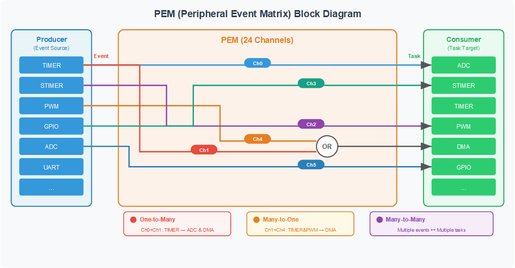
Core Concepts
| Concept | Description |
|---|---|
| Event | An interrupt-like signal sent out by a peripheral. |
| Task | A signal received by a peripheral, which can be connected to any event signal. The task signal is treated as an enable or trigger signal. |
| Channel | Each PEM channel independently maps one event to one task. The channels vary in different chips, refer the definition pem_chn_e in pem.h. |
Compared to Traditional Interrupt
Taking "the timer triggers an ADC sample once every second" as an example, the differences between the two implementation methods are as follows:
| No PEM | Use PEM | |
|---|---|---|
| Workflow | Timer interrupt -> CPU enters ISR -> Manual call to start ADC -> Exit ISR | Timer event -> PEM channel -> ADC task; the entire process is handled automatically by hardware |
| CPU Involvement | Requires the CPU to enter and exit the ISR on each trigger | No CPU involvement required |
| Latency | Interrupt response + context switch | Pure hardware latency |
| Risk of Nested Interrupts | ISRs may be interrupted by higher-priority interrupts | Not affected by interrupt priority |
Note
- PEM can only route trigger/enable signals. Actual data transfer between peripherals still requires DMA or MCU to write/read data.
Multi-Channel Routing
- One-to-many: One event can be routed to multiple tasks through multiple channels.
- Many-to-one: Multiple events can be routed to the same task through multiple channels. PEM performs an "OR" logic on events without arbitration. The peripheral itself needs to handle the case when multiple events arrive simultaneously.
- Many-to-many: Achieved by using multiple channels.
Usage Flow
To use PEM, first complete the initialization of the peripheral itself and then configure the PEM channel to connect the two. The complete process is as follows:
1. pem_init() — enable the PEM module
2. Initialize the event source peripheral — Configure the operating modes and interrupts for peripheral devices (such as setting the Stimer period and enabling interrupts)
3. <peripheral>_set_pem_event() — Connect a specific event signal from a peripheral to a PEM channel
4. Initialize the task target peripheral — Configure the operating mode of peripheral devices (such as ADC clock, channels, and sampling parameters)
5. <peripheral>_set_pem_task() — Connect the PEM channel to a task signal on the peripheral
6. pem_chn_en() — Enable the channel; the router takes effect
7. Start the event source — Start automatically triggering the task
Example: Stimer Interrupt Triggers a Single ADC Sample
/* 1. Enable PEM */
pem_init();
/* 2. Initialize the event source peripheral: Configure the timer to generate an interrupt once every second */
stimer_set_irq_capture(stimer_get_tick() + SYSTEM_TIMER_TICK_1S);
stimer_set_irq_mask(FLD_SYSTEM_IRQ_MASK);
plic_interrupt_enable(IRQ_SYSTIMER);
core_interrupt_enable();
/* 3. stimer_set_pem_event() — Connect the STIMER's timer interrupt event to the PEM channel */
stimer_set_pem_event(PEM0, STIMER_EVENT_TRIG_POS);
/* 4. Initialize the target peripheral for the task: Configure ADC parameters */
adc_init(ADC0, NDMA_M_CHN); // ADC initialization(NDMA single channel)
adc_set_clk(ADC0, ADC_CLK_4M); // Clock configuration
adc_set_sample_chn(ADC0, ADC_CHN0); // sampling channel selection
/* 5. adc_set_pem_task() — Connect the ADC's single-sample task to the same PEM channel */
adc_set_pem_task(ADC0, PEM0, ADC_TASK_SINGLE_ADC_TRIG);
/* 6. Enable PEM channel */
pem_chn_en(PEM0);
// After that, the Stimer generates an interrupt once per second, automatically triggering the ADC to perform a sample via the PEM.
The specific API parameters and initialization methods for peripherals vary by chip; please refer to the demo project and header files for the corresponding chip.
Overview of API
Core API
| Function | Description |
|---|---|
pem_init() |
Enable the PEM module (reset + clock on) |
pem_chn_en(chn) |
Enable the specified channel; event-to-task routing begins. |
pem_chn_dis(chn) |
Disable specified channels |
Peripheral PEM Interface
Every PEM-compatible peripheral provides two interfaces, named according to a uniform convention:
- event configuration:
<peripheral>_set_pem_event() - task configuration:
<peripheral>_set_pem_task()
For example, the STIMER provides stimer_set_pem_event() / stimer_set_pem_task(),the ADC provides adc_set_pem_event() / adc_set_pem_task(), and so on.
How to determine whether a peripheral supports PEM? Check the enumerations pem_event_module_sel_e and pem_task_module_sel_e. You can search for pem_event or pem_task in the corresponding peripheral header file to view the relevant function declarations. For details on which event/task signals and function parameters are provided, please refer to the enumeration definitions in the corresponding peripheral header file.
I3C
I3C Module Overview
| Chip | I3C Controllers |
|---|---|
| TL322x | I3C0, I3C1 (2 channels) |
| TL521x | I3C0 (1 channel) |
Introduction to the I3C Protocol
I3C (Improved Inter-Integrated Circuit) is a next-generation two-wire serial bus developed by the MIPI Alliance. Building on I2C, it enhances speed and functionality and is primarily intended for low-speed peripherals such as sensors.
Key Features:
- Higher Speed: The address segment is open-drain, while the data segment can switch to push-pull. SDR (Single Data Rate) mode is far faster than I2C, with a maximum rate of up to 12 Mbps
- Dynamic Addressing: During bus initialization, the Controller assigns each Target a dynamic 7-bit address through the DAA (Dynamic Address Assignment) process, eliminating the need for hardware jumpers
- Command Mechanism: CCC (Common Command Code) supports both broadcast and directed commands for bus configuration and management
- In-Band Interrupt (IBI): Targets send interrupt requests through the bus itself (optionally with payload data), eliminating the need for a dedicated interrupt pin
- Hot-Join (HJ): Devices powered on later can request to join the bus at any time
- Multi-Master Support: Supports Master Request and role switching; a
Master Capable Targetcan take over the bus - I2C Compatibility: Supports I2C-style static addresses, allowing an I3C controller to connect to an I2C bus
- Application Scenarios: Sensor hubs, automotive, consumer electronics, I/O expansion, etc.
I3C Bus Topology and Node Roles
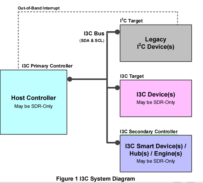
| Node Role | Description |
|---|---|
| Controller (Master) | Bus scheduler; initiates DAA, sends CCCs, schedules all read/write transfers, and responds to IBI/HJ/MR events |
| Target (Slave) | Scheduled party; monitors the bus; obtains a dynamic address after DAA and responds by address/CCC |
| Master Capable Target | Once declared, it can request to take over the bus and become the Controller (see Section Transfer and Bus Control / Role Switch (TRANSFER_BUS_CONTROL) for the Demo) |
| Legacy I2C device | Accessed via static address; coexists with I3C devices (select I3C_TYPEI2C for bus_type during transfers) |
I3C Frame Structure (SDR)
One I3C SDR frame consists of multiple "8-bit bytes + the 9th bit". The unified frame structure is as follows:
S | 7-bit address | R/W | 9th bit (ACK) | 8-bit data | 9th bit | 8-bit data | 9th bit | ... | P (Stop)
| Field | Description |
|---|---|
| S / Sr / P | Start / Repeated Start / Stop condition |
| 7-bit address + R/W | The address segment is sent open-drain and supports arbitration; 0x7E is the broadcast address (used for broadcast CCCs and Auto-IBI polling) |
| Data | The data segment can be sent push-pull |
| 9th bit | The 9th bit after the address byte is the ACK (Target response); the meaning of the 9th bit after a data byte depends on the read/write direction (see below) |
Meaning of the 9th bit in the write sequence (Controller → Target):
When writing data, the 9th bit after a data byte is the parity bit (P): it is driven by the sender (Controller) after performing odd parity over the preceding 8 bits of data, and the Target uses it to verify the correctness of the received data.
Meaning of the 9th bit in the read sequence (Target → Controller):
When reading data, the 9th bit after a data byte is the terminate bit (T): it can be used to terminate the transfer from either the Master side or the Slave side. On the rising edge of the 9th clock, if the Slave pulls it low, it indicates that the Slave is signaling termination; if the Slave leaves it high, the read can continue.
Info
- The 9th bit after the address byte is still the Target's ACK/NACK response (same as I2C); the 9th bit after a data byte serves as parity for the write direction and read-termination control for the read direction. This timing is handled automatically by hardware and requires no user intervention.
Dynamic Address Assignment and UID/BCR/DCR
- Static Address: Fixed at the factory, used during the bus initialization stage before DAA (the Demo slave device defaults to
0x1E). - Dynamic Address: A 7-bit address assigned by the Controller during the DAA (ENTDAA) process; all subsequent bus communication uses the dynamic address.
- UID (48-bit Unique Identifier): The device's unique factory identifier, containing the vendor ID (16-bit) and part number; reported to the Controller during DAA.
- BCR (Bus Characteristics Register): Bus characteristics, indicating device capabilities (whether IBI/HJ/MR is supported, etc.).
- DCR (Device Characteristics Register): Device characteristics, indicating the device type.
After the Controller executes i3c_master_process_daa(), it records the dynamic address assigned to each slave device along with the device-reported 48-bit UID, BCR, and DCR into the global table g_dev_list[chn][], which the user can read and use directly.
CCC Commands and the IBI Mechanism
- CCC (Common Command Code): Bus-level commands, divided into broadcast (all Targets respond) and directed (a specified Target responds). The timing is completed by hardware working with software in segmented transmission. For details on supported CCCs, refer to the datasheet.
- IBI (In-Band Interrupt): An event actively initiated by a Target, in three categories: normal IBI, Hot-Join, and Master Request. The Controller identifies the type in an interrupt and responds with ACK/NACK. See the relevant sections below for details.
I3C Driver and Demo File Structure
Driver File Structure
TL322x is used as an example; other chips share the same structure.
| File | Description |
|---|---|
chip/tl322x/drivers/i3c.h |
Driver header file; defines enums, structures, API declarations, and inline functions |
chip/tl322x/drivers/i3c.c |
Driver implementation: initialization, DAA, read/write transfers, IBI, DMA, baud rate calculation, etc. |
chip/tl322x/drivers/reg_include/i3c_reg.h |
Register address and bit-field definitions (see the chip datasheet for register meanings) |
Demo File Structure
The I3C Demo is located in tl_platform_src/demo/vendor/I3C_Demo/:
| File | Corresponding Test Mode | Description |
|---|---|---|
app_no_dma_master.c |
NO_DMA_MASTER |
Master node, CPU-based transmit/receive + IBI handling |
app_no_dma_slave.c |
NO_DMA_SLAVE |
Slave node, CPU-based transmit/receive + IBI notification |
app_dma_master.c |
DMA_MASTER |
Master node, DMA-based transmit/receive |
app_dma_slave.c |
DMA_SLAVE |
Slave node, DMA-based transmit/receive |
other_functions/app_transfer_bus_control.c |
TRANSFER_BUS_CONTROL |
Combined CCC usage + role switching |
other_functions/app_timing_control.c |
TIMING_CONTROL |
SETXTIME/GETXTIME timing control |
other_functions/app_target_reset.c |
TARGET_RESET |
RSTACT target reset |
other_functions/app_group_address.c |
GROUP_ADDRESS |
SETGRPA group address |
other_functions/app_mapped_address.c |
MAPPED_ADDRESS |
SETDASA/SETAASA + mapped address |
main.c |
- | Program entry; calls user_init() and main_loop() |
Mode switching (demo/vendor/common/common/app_config/i3c_app_config.h):
#define NO_DMA_MASTER 0
#define NO_DMA_SLAVE 1
#define DMA_MASTER 2
#define DMA_SLAVE 3
#define TRANSFER_BUS_CONTROL 4
#define TIMING_CONTROL 5
#define TARGET_RESET 6
#define GROUP_ADDRESS 7
#define MAPPED_ADDRESS 8
#define I3C_MODE NO_DMA_MASTER /* Modify this to select the use case */
/* Pin definitions (chip specific) */
#if defined(MCU_CORE_TL322X)
#define I3C_GPIO_SDA_PIN GPIO_FC_PE0
#define I3C_GPIO_SCL_PIN GPIO_FC_PE2
#elif defined(MCU_CORE_TL521X)
#define I3C_GPIO_SDA_PIN GPIO_FC_PE0
#define I3C_GPIO_SCL_PIN GPIO_FC_PE1
#endif
- Test mode: The
I3C_MODEmacro selects the use case to compile; each source file uses#if(I3C_MODE == xxx)conditional compilation at the top. - Pins:
I3C_GPIO_SDA_PIN/I3C_GPIO_SCL_PINdefine SDA/SCL; wiring is master-to-slave board SDA↔SDA, SCL↔SCL, with a common GND. - Other parameters: Some use cases additionally use
MODE/CONTROLLER_MODEmacros inside the files to distinguish master/slave.
I3C Module Initialization and Configuration
Initialization Parameters (i3c_master_config_t / i3c_slave_config_t)
Master initialization parameters:
i3c_master_config_t g_master_config;
g_master_config.master_en = I3C_MASTER_ON; // Master mode enable
g_master_config.timeout_dis = 1; // Disable frame timeout warning (recommended to set to 1)
g_master_config.baudrate_hz.i2c_baud = 1000000; // I2C-compatible mode baud rate 1MHz
g_master_config.baudrate_hz.i3c_pushpull_baud = 6000000; // I3C push-pull mode baud rate 6MHz
g_master_config.baudrate_hz.i3c_opendrain_baud = 1000000; // I3C open-drain mode baud rate 1MHz
g_master_config.opendrain_stop_en = false; // Whether to send STOP at open-drain speed
g_master_config.clk_src.clk_src = CLK_BASEBAND_PLL_144M; // Clock source
g_master_config.clk_src.clk_src_div = 6; // Divider (144M/6 = 24M)
| Field | Value | Description |
|---|---|---|
master_en |
I3C_MASTER_OFF/ON/CAPABLE |
Master enable; CAPABLE declares master capability while in slave mode |
timeout_dis |
true / false | Disables the timeout to prevent ERRWARN; recommended to set to 1 |
baudrate_hz |
- | Three baud rates: I2C / I3C push-pull / I3C open-drain |
opendrain_stop_en |
true / false | Whether the STOP is issued at open-drain speed |
clk_src |
CLK_RC_24M / CLK_XTAL_24M / PLL frequencies |
Controller clock source; the divided frequency must match the target baud rate |
Slave initialization parameters:
i3c_slave_config_t g_slave_config;
g_slave_config.is_master_capable = 0; // Whether the device supports taking over the bus as Master
g_slave_config.static_addr = 0x1E; // Static address (used for identification before DAA)
g_slave_config.offline = 0; // Whether to wait for bus silence to ensure SDR tracking; used to control the slave "temporarily leaving the bus and later rejoining with the previously assigned dynamic address" without re-running the full ENTDAA address assignment process.
g_slave_config.is_hotjoin = 0; // Whether to issue a Hot-Join request immediately on power-up
g_slave_config.clk_src.clk_src = CLK_BASEBAND_PLL_144M;
g_slave_config.clk_src.clk_src_div = 6;
Interrupt Enable and Handling
Common Master interrupt masks (i3c_master_set_irq_mask()):
| Mask | Trigger Condition | Purpose |
|---|---|---|
I3C_MASTER_ARBITRATIONWON_FLAG |
A Target event wins arbitration on the address header | Identify IBI/HJ/MR and respond |
I3C_MASTER_SLAVESTART_FLAG |
A Target pulls SDA low to request service | Trigger Auto-IBI (START+0x7E) to retrieve the event |
I3C_MASTER_COMPLETE_FLAG |
A transfer/IBI data segment completes | Wrap up (send STOP), notify application layer |
I3C_MASTER_SLAVE2MASTER_FLAG |
Slave-to-master role switch completes | Role-switch use case |
I3C_MASTER_RXREADY_FLAG |
RX FIFO reaches watermark | Read received data |
I3C_MASTER_TXTEADY_FLAG |
TX FIFO reaches watermark | Fill transmit data |
Common Slave interrupt masks (i3c_slave_set_irq_mask()):
| Mask | Trigger Condition | Purpose |
|---|---|---|
I3C_SLAVE_DYNAMIC_ADDRCHANGED_FLAG |
A dynamic address is assigned | Wait for DAA to complete |
I3C_SLAVE_MATCHED_FLAG |
Local address is matched | Record the start of an addressing sequence |
I3C_SLAVE_BUSSTOP_FLAG |
Bus stop detected | Combined with MATCHED to determine transfer end |
I3C_SLAVE_RXREADY_FLAG |
RX FIFO reaches watermark | Read received data / CCC data |
I3C_SLAVE_TXREADY_FLAG |
TX FIFO reaches watermark | Fill transmit data |
I3C_SLAVE_EVENTSENT_FLAG |
IBI/HJ/MR event has been sent | Confirm the event was initiated successfully |
I3C_SLAVE_RECEIVED_CCC_FLAG |
A CCC that is not automatically handled by hardware is received | Distinguish normal data from CCC data |
I3C_SLAVE_CCCHANDLED_FLAG |
A CCC was auto-handled by hardware | Distinguish transfer completion in the DMA use case |
I3C_SLAVE_TGTRST_FLAG |
Target reset received | Target-reset use case |
Dynamic Address Assignment (DAA)
unsigned char g_address_list[8] = {0x30, 0x31, 0x32, 0x33, 0x34, 0x35, 0x36, 0x37};
result = i3c_master_process_daa(I3C_CHN, g_address_list, 8);
if (result != I3C_STATUS_SUCCESS) {
while(1); // Address assignment failed (e.g., no slave devices / insufficient addresses)
}
- The driver automatically executes the ENTDAA process, taking addresses from
g_address_listin order and assigning them to the slave devices responding on the bus. - Each time a slave device is discovered, its UID (
vendor_id+part_number), BCR, and DCR are recorded intog_dev_list[I3C_CHN][]. - If the number of devices exceeds the address table length or the limit (10 devices),
I3C_STATUS_SLAVE_COUNT_EXCEEDis returned and a STOP is issued automatically. - Subsequent communication uniformly uses the assigned dynamic address (the Demo uses
g_address_list[0], i.e., the first slave device).
The specific protocol procedure is as follows:
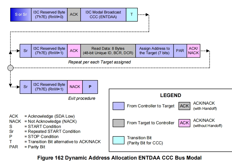
IBI Mechanism
An IBI is an interrupt request actively initiated by an I3C slave (Target). In I2C, only the master can poll; in I3C, the IBI allows a slave to actively contend for the bus to report an event. Core essence: after START, the slave performs bus arbitration in the address header, and the winning slave sends its address to the master.
The Master responds according to the actual situation via the enum i3c_ibi_response_e:
| enum | Description |
|---|---|
I3C_IBI_RESPACK |
Follow the IBI rules registered by i3c_master_register_ibi(), accepting both cases with and without the mandatory byte |
I3C_IBI_RESPNACK |
Respond with NACK |
I3C_IBI_RESPACK_MANDATORY |
Regardless of the IBI rules registered by i3c_master_register_ibi(), always accept with the mandatory byte |
Concrete implementation:
void i3c0_irq_handler(void){
unsigned int status_flags = i3c_master_get_irq_status(I3C_CHN);
unsigned char rx_count = 0;
i3c_master_get_fifo_count(I3C_CHN, &rx_count, NULL);
i3c_ibi_type_e ibi_type;
/* ① IBI event: won arbitration on the address header */
if(status_flags & I3C_MASTER_ARBITRATIONWON_FLAG){
i3c_master_clr_irq_status(I3C_CHN, I3C_MASTER_ARBITRATIONWON_FLAG);
ibi_type = i3c_master_get_ibi_type(I3C_CHN); // Event type: normal / Hot-Join / Master Request
switch (ibi_type){
case I3C_IBI_NORMAL: g_ibi_normal_address = i3c_get_ibi_address(I3C_CHN); break;
case I3C_IBI_HOTJOIN: g_ibi_hotjoin_address = i3c_get_ibi_address(I3C_CHN); break;
case I3C_IBI_MASTERREQUEST: g_ibi_master_req_address = i3c_get_ibi_address(I3C_CHN); break;
default: break;
}
/* Cases that require manual ACK/NACK: the state machine is in IBIACK */
if(i3c_master_get_state(I3C_CHN) == I3C_MASTER_STATE_IBIACK){
i3c_master_emit_ibi_response(I3C_CHN, I3C_IBI_RESPACK); // or RESPNACK
}else{
/* IBI data segment complete (no data payload): send STOP and notify application layer */
if((rx_count == 0) && (status_flags & I3C_MASTER_COMPLETE_FLAG)){
i3c_master_clr_irq_status(I3C_CHN, I3C_MASTER_COMPLETE_FLAG);
i3c_master_emit_request(I3C_CHN, I3C_REQUEST_EMITSTOP);
g_is_ibi_normal_flag = 1;
}else{
g_ibiwon_has_data = 1; // IBI carries data
i3c_master_set_irq_mask(I3C_CHN, I3C_MASTER_RXREADY_FLAG);
}
}
return;
}
/* ② IBI data payload read */
if(status_flags & I3C_MASTER_RXREADY_FLAG){
if(g_ibiwon_has_data){
while(rx_count != 0){
g_ibi_buff[g_ibi_buff_size++] = reg_i3c_mrdatab_0(I3C_CHN);
rx_count--;
}
}
}
/* ③ Bus idle polling: when a Target pulls SDA low, automatically START+0x7E to retrieve the event */
if(status_flags & I3C_MASTER_SLAVESTART_FLAG){
i3c_master_clr_irq_status(I3C_CHN, I3C_MASTER_SLAVESTART_FLAG);
i3c_master_emit_request(I3C_CHN, I3C_REQUEST_AUTOIBI);
return;
}
/* ④ IBI data segment completion wrap-up */
if(g_ibiwon_has_data && (status_flags & I3C_MASTER_COMPLETE_FLAG)){
i3c_master_clr_irq_status(I3C_CHN, I3C_MASTER_COMPLETE_FLAG);
i3c_master_emit_request(I3C_CHN, I3C_REQUEST_EMITSTOP);
g_is_ibi_normal_flag = 1;
g_ibiwon_has_data = 0;
g_ibi_buff_size = 0;
i3c_master_clr_irq_mask(I3C_CHN, I3C_MASTER_RXREADY_FLAG);
}
}
Key points of interrupt handling:
1. Use I3C_MASTER_SLAVESTART_FLAG to detect whether a Slave has initiated an IBI request; the Master then issues a request for the Slave to send its ID.
2. I3C_MASTER_ARBITRATIONWON_FLAG indicates the address-header arbitration was won and the IBI request interrupt is raised; the Master responds via i3c_master_emit_ibi_response(I3C_CHN, I3C_IBI_RESPACK).
3. If the IBI request from the Slave carries a mandatory byte, the Master receives it via the I3C_MASTER_RXREADY_FLAG interrupt.
Master Use Case (NO_DMA_MASTER)
Transfer Parameter Configuration (i3c_master_transfer_t)
i3c_master_transfer_t g_master_transfer;
g_master_transfer.slave_address = g_address_list[0]; // Target dynamic address
g_master_transfer.subaddress = NULL; // Sub-address (register address), optional
g_master_transfer.subaddress_size = 0; // Sub-address length (max 4)
g_master_transfer.data = g_master_txbuff; // Data buffer
g_master_transfer.data_size = sizeof(g_master_txbuff);
g_master_transfer.bus_type = I3C_TYPEI3CSDR; // SDR or I2C
g_master_transfer.flags = I3C_TRANSFER_DEFAULT_FLAG; // Send START at the beginning, STOP at the end
g_master_transfer.ibi_response = I3C_IBI_RESPACK_MANDATORY;
g_master_transfer.direction = I3C_WRITE; // or I3C_READ
result = i3c_master_write(I3C_CHN, &g_master_transfer); // Use i3c_master_read() for reads
Common flags values:
| Flag | Meaning |
|---|---|
I3C_TRANSFER_DEFAULT_FLAG |
Send START at the beginning and STOP at the end (normal transfer) |
I3C_TRANSFER_NOSTOP_FLAG |
Do not send STOP |
I3C_TRANSFER_STARTWITH_BROADCAST_ADDR |
Start with the 0x7E broadcast address |
I3C_TRANSFER_NOSTART_FLAG |
Do not send start condition, address, or sub-address (bus is already set up to continue a transfer) |
Initialization and Main Loop Scheduling
Procedure:
| Step | Key Interfaces | Description |
|---|---|---|
| 1 | i3c_master_set_pin() / i3c_master_init() |
Pin and hardware initialization |
| 2 | i3c_master_set_irq_mask() + plic_interrupt_enable() |
Enable interrupts (including IBI-related ones) |
| 3 | i3c_master_process_daa() |
DAA assigns dynamic addresses |
| 4 | i3c_master_register_ibi() |
Register IBI rules |
| 5 | main_loop() |
Loop: write → wait for slave IBI → read → verify |
Main loop example (NO_DMA_MASTER):
void main_loop (void)
{
g_master_txbuff[0]++;
/* ---- Step 1: write 16 bytes to the slave ---- */
g_master_transfer.slave_address = g_address_list[0];
g_master_transfer.data = g_master_txbuff;
g_master_transfer.data_size = sizeof(g_master_txbuff);
g_master_transfer.bus_type = I3C_TYPEI3CSDR;
g_master_transfer.flags = I3C_TRANSFER_DEFAULT_FLAG;
g_master_transfer.direction = I3C_WRITE;
result = i3c_master_write(I3C_CHN, &g_master_transfer);
/* ---- Step 2: wait for the slave's IBI (data is ready) ---- */
while(!g_is_ibi_normal_flag);
g_is_ibi_normal_flag = 0;
/* ---- Step 3: read 16 bytes and verify ---- */
g_master_transfer.data = g_master_rxBuff;
g_master_transfer.data_size = sizeof(g_master_rxBuff);
g_master_transfer.direction = I3C_READ;
result = i3c_master_read(I3C_CHN, &g_master_transfer);
for (unsigned char i = 0; i < 16; i++) {
if (g_master_rxBuff[i] != g_master_txbuff[i]) while(1); // Verification failed
}
}
Info
- The Demo's three-step "write → wait for IBI → read" is a common I3C slave-ready handshake: after receiving the data, the Slave notifies the Master via IBI that "you can come read now"; after the Master sets
g_is_ibi_normal_flagin the interrupt, it continues with the read operation.
Slave Use Case (NO_DMA_SLAVE)
Initialization and Waiting for the Dynamic Address
void user_init(void)
{
i3c_slave_set_pin(I3C_CHN, I3C_GPIO_SDA_PIN, I3C_GPIO_SCL_PIN);
g_slave_config.is_master_capable = 0;
g_slave_config.static_addr = 0x1E; // Static address, used for identification before DAA
g_slave_config.offline = 0;
g_slave_config.is_hotjoin = 0;
g_slave_config.clk_src.clk_src = CLK_BASEBAND_PLL_144M;
g_slave_config.clk_src.clk_src_div = 6;
i3c_slave_init(I3C_CHN, &g_slave_config);
i3c_slave_set_irq_mask(I3C_CHN, I3C_SLAVE_RXREADY_FLAG | I3C_SLAVE_DYNAMIC_ADDRCHANGED_FLAG |
I3C_SLAVE_MATCHED_FLAG | I3C_SLAVE_EVENTSENT_FLAG |
I3C_SLAVE_BUSSTOP_FLAG);
g_txfifo_size = i3c_get_txfifo_size(I3C_CHN); // Query TX FIFO depth
while(!g_dynamic_addr_flag){} // Wait for the Master to complete DAA
g_dynamic_addr_flag = 0;
}
Info
- Slave initialization does not start any scheduling; once complete, the device monitors the bus waiting for the Master to send a frame header. After DAA completes (
DYNAMIC_ADDRCHANGED), the device can participate in communication.
Interrupt Handling Flow
The Slave is the "passive responder"; the core of its interrupt handling is "address match → receive/transmit data → use match + stop to determine completion":
| Interrupt | What to do in the interrupt |
|---|---|
I3C_SLAVE_MATCHED_FLAG |
Record the address match as the start marker of this transfer |
I3C_SLAVE_RXREADY_FLAG |
Drain the RX FIFO: normal data goes into g_slave_rxbuff, CCC data (with g_ccc_receives_flag set) goes into g_ccc_buff |
I3C_SLAVE_TXREADY_FLAG |
Fill the TX FIFO; the last byte must be written as the end byte (i3c_slave_write_end_byte()) |
I3C_SLAVE_BUSSTOP_FLAG |
Combined with MATCHED: determine the end of a transfer, set the completion flag based on receive/transmit counters |
I3C_SLAVE_EVENTSENT_FLAG |
Confirm the IBI/HJ/MR event has been sent |
I3C_SLAVE_DYNAMIC_ADDRCHANGED_FLAG |
Dynamic address change (caused by DAA/CCC), set the waiting flag |
Key points for transmission: After the master initiates a read, the Slave writes data into the TX FIFO in the TXREADY interrupt; the last byte must be written via i3c_slave_write_end_byte() as the "end byte". In the Demo, the I3C_SLAVE_TXREADY_FLAG mask is first enabled, then disabled after filling completes to prevent false triggers.
Completion determination: The recommended MATCHED + BUSSTOP combination (Demo logic):
if(g_address_match_flag && (status_flags & I3C_SLAVE_BUSSTOP_FLAG)){
i3c_slave_clr_irq_status(I3C_CHN, I3C_SLAVE_BUSSTOP_FLAG);
if(g_transfer_rx_size) g_slave_rx_completion_flag = 1; // This frame is a write
else if(g_transfer_tx_size) g_slave_tx_completion_flag = 1; // This frame is a read
/* Reset counters and flags, prepare for the next frame */
}
Initiating an IBI Event
The Slave proactively notifies the Master (e.g., "data is ready") using an IBI with a data payload:
/* Main loop: receive data → echo → IBI notify the Master that it can read */
memcpy(g_slave_txbuff, g_slave_rxbuff, TRANSFER_LEN);
unsigned char ibi_data = g_slave_rxbuff[0]; // IBI data payload (1 byte)
i3c_slave_request_ibi_with_data(I3C_CHN, &ibi_data, 1);
while(!g_slave_request_flag){} // Wait for EVENTSENT
g_slave_request_flag = 0;
i3c_slave_set_irq_mask(I3C_CHN, I3C_SLAVE_TXREADY_FLAG); // Enable transmission, wait to be read by the Master
while(!g_slave_tx_completion_flag){}
g_slave_tx_completion_flag = 0;
| Interface | Description |
|---|---|
i3c_slave_request_event(chn, event) |
Send a normal event: I3C_SLAVE_EVENT_IBI / MASTER_REQ / HOTJOIN_REQ |
i3c_slave_request_ibi_with_data(chn, data, size) |
Send an IBI with a data payload; data[0] is the data; supports up to 8 bytes of payload |
DMA Transfers
Principle: In DMA mode, hardware moves data automatically, reducing CPU load.
Usage steps:
| Step | Interface | Description |
|---|---|---|
| 1 | i3c_set_tx_dma_config() / i3c_set_rx_dma_config() |
Bind TX/RX DMA channels (each uses an independent channel) |
| 2 | i3c_master_write_dma() / i3c_master_read_dma() |
Master DMA transfer |
| 3 | i3c_slave_set_tx_dma() / i3c_slave_set_rx_dma() |
Slave DMA transmit/receive (must be re-armed during initialization and after each reception completes) |
DMA_MASTER
#define I3C_TX_DMA_CHN DMA0
#define I3C_RX_DMA_CHN DMA1
i3c_set_tx_dma_config(I3C_CHN, I3C_TX_DMA_CHN);
i3c_set_rx_dma_config(I3C_CHN, I3C_RX_DMA_CHN);
/* Master DMA write/read (data buffers must be 4-byte aligned) */
result = i3c_master_write_dma(I3C_CHN, &g_master_transfer);
while(!g_dma_completed_flag){} /* Wait for the COMPLETE interrupt */
g_dma_completed_flag = 0;
result = i3c_master_read_dma(I3C_CHN, &g_master_transfer);
while(!g_dma_completed_flag);
g_dma_completed_flag = 0;
SLAVE_DMA
This section mainly describes the differences between DMA slave mode and non-DMA slave mode (NO_DMA_SLAVE) in data transmission and reception.
Initialization:
/* ① Bind DMA channels (TX/RX each use an independent channel) */
#define I3C_TX_DMA_CHN DMA0
#define I3C_RX_DMA_CHN DMA1
i3c_set_tx_dma_config(I3C_CHN, I3C_TX_DMA_CHN);
i3c_set_rx_dma_config(I3C_CHN, I3C_RX_DMA_CHN);
/* ② Interrupt masks: no RXREADY/TXREADY, CCCHANDLED added */
i3c_slave_set_irq_mask(I3C_CHN, I3C_SLAVE_MATCHED_FLAG | I3C_SLAVE_BUSSTOP_FLAG |
I3C_SLAVE_EVENTSENT_FLAG | I3C_SLAVE_DYNAMIC_ADDRCHANGED_FLAG |
I3C_SLAVE_CCCHANDLED_FLAG);
/* ③ After DAA completes, pre-arm the RX DMA: data is written at buffer + 4 offset; the first 4 bytes are reserved for DMA to write back the receive count */
while(!g_dynamic_addr_flag){}
g_dynamic_addr_flag = 0;
i3c_slave_set_rx_dma(I3C_CHN, g_slave_rxbuff + 4, TRANSFER_LEN);
g_rx_buff_flag = g_slave_rxbuff; /* Points to the buffer base address; read the receive byte count written back by DMA */
Main loop:
Note: The Slave can fill data into DMA in advance and send an IBI request; when the Master issues a read request, the TX DMA starts working.
void main_loop (void)
{
while(!g_slave_rx_completion_flag){} /* Wait for one DMA reception to complete */
g_slave_rx_completion_flag = 0;
memcpy(g_slave_txbuff, g_slave_rxbuff + 4, TRANSFER_LEN); /* Echo */
*(unsigned int*)g_rx_buff_flag = 0; /* Clear the DMA write-back count, prepare for the next reception */
i3c_slave_set_tx_dma(I3C_CHN, g_slave_txbuff, TRANSFER_LEN); /* Configure the whole TX at once; DMA automatically appends the end bit */
unsigned char ibiData = g_slave_rxbuff[4]; /* IBI notifies the Master that data is ready */
i3c_slave_request_ibi_with_data(I3C_CHN, &ibiData, 1);
while(!g_slave_request_flag){}
g_slave_request_flag = 0;
while(!g_slave_tx_completion_flag){} /* Wait until the Master has finished reading */
g_slave_tx_completion_flag = 0;
}
Interrupt handling (receive/transmit completion determination):
if(g_address_match_flag && (status_flags & I3C_SLAVE_BUSSTOP_FLAG)){
i3c_slave_clr_irq_status(I3C_CHN, I3C_SLAVE_BUSSTOP_FLAG);
/* Reception complete: determined by the DMA write-back count (write_num_en=1; DMA writes the received byte count into the 4 bytes before the target address, i.e., the buffer base address) */
if(*(unsigned int*)g_rx_buff_flag != 0){
g_slave_rx_completion_flag = 1;
i3c_slave_set_rx_dma(I3C_CHN, g_slave_rxbuff + 4, TRANSFER_LEN); /* Re-arm the next RX */
}
/* Transmission complete: only set for non-CCC frames (CCCs are auto-handled by hardware, which sets CCCHANDLED) */
if(!g_slave_ccc_handled_flag){
g_slave_tx_completion_flag = 1;
}
g_address_match_flag = 0;
g_slave_ccc_handled_flag = 0;
}
Usage notes:
1. The head of the receive buffer must reserve 4 bytes (g_slave_rxbuff[16+4]): RX DMA data is written at a +4 offset, and the hardware writes the number of bytes received in this transfer at the base address (corresponding to the RX DMA configuration write_num_en=1, which writes into the 4 bytes before the target address).
2. After each DMA reception completes, i3c_slave_set_rx_dma() must be called again in the interrupt to pre-arm the next reception.
3. In DMA mode, the end bit of the data is handled automatically by the driver during repacking; there is no need to manually call i3c_slave_write_end_byte() as in no-DMA mode.
4. TX/RX use independent DMA channels (Demo: TX=DMA0, RX=DMA1); the transmit buffer is recommended to be 4-byte aligned.
no-DMA/DMA Demo: dynamic address assignment → write → IBI → read timing is as follows

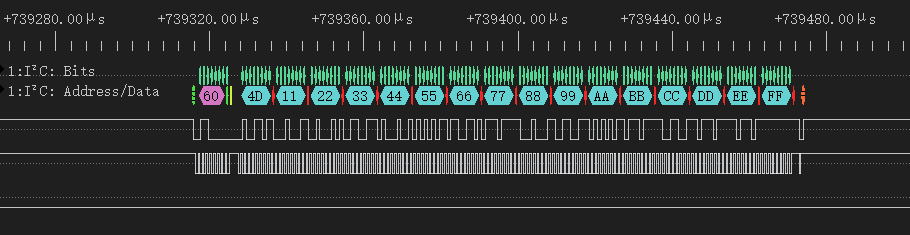
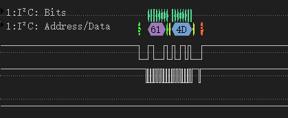
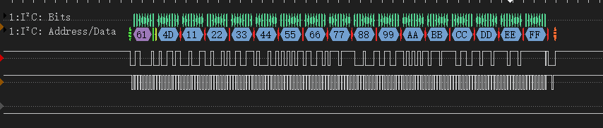
Advanced Feature Use Cases
Using CCC Commands
Principle: CCCs are divided into broadcast and directed types. Broadcast commands (such as RSTDAA, SETAASA) are responded to by all Targets; directed commands require a specified target address. For supported CCCs, refer to the datasheet; for the specific transmission timing, refer to the comments in i3c.h.
CCCs covered by the Demo:
| CCC | Command Code | Type | Function | Demo Location |
|---|---|---|---|---|
| ENEC / DISEC | 0x00/0x80, 0x01/0x81 | Broadcast/Directed | Enable/disable target events (IBI/HJ/MR) | app_transfer_bus_control.c |
| RSTDAA | 0x06 | Broadcast | Reset all dynamic addresses | - |
| DEFTGTS | 0x08 | Broadcast | Define the target device table | app_transfer_bus_control.c |
| SETXTIME | 0x28/0x98 | Broadcast/Directed | Set timing control | app_timing_control.c |
| GETXTIME | 0x99 | Directed | Read timing control status | app_timing_control.c |
| SETAASA | 0x29 | Broadcast | All devices adopt static addresses | app_mapped_address.c |
| RSTACT | 0x2A/0x9A | Broadcast/Directed | Target reset | app_target_reset.c |
| SETGRPA | 0x9B | Directed | Set group address | app_group_address.c |
| SETDASA | 0x87 | Directed | Assign dynamic addresses to static-address devices | app_mapped_address.c |
| GETUID | 0x8D | Directed | Read the 48-bit UID | - |
| GETBCR / GETDCR | 0x8E / 0x8F | Directed | Read the bus/device characteristics registers | - |
| GETSTATUS | 0x90 | Directed | Read target status (2 bytes) | app_transfer_bus_control.c |
| GETACCCR | 0x91 | Directed | Get the active controller | app_transfer_bus_control.c |
| GETCAPS | 0x95 | Directed | Read capabilities (4 bytes, may carry sub-commands) | app_transfer_bus_control.c |
Group Address (GROUP_ADDRESS)
Principle: Use SETGRPA to add multiple Targets to the same group; afterward, accessing them by group address writes to multiple devices at once.
Procedure:
| Step | Description |
|---|---|
| 1 | The Master performs DAA |
| 2 | Send SETGRPA (0x9B) to each target: 0x7E + 0x9B (NOSTOP) + restart + target addr/w/ack, then a directed write of the group address <<1 |
| 3 | Write data using the group address (right-shifted by 1) as slave_address; all targets in the group receive it simultaneously |
/* Set group address 0x08 for the target device */
unsigned char subaddress[1] = {0x9b};
g_master_transfer.slave_address = 0x7e;
g_master_transfer.data = subaddress;
g_master_transfer.data_size = 1;
g_master_transfer.flags = I3C_TRANSFER_NOSTOP_FLAG; /* Step 1: send the CCC without STOP */
result = i3c_master_write(I3C_CHN, &g_master_transfer);
g_master_transfer.slave_address = g_address_list[0]; /* Step 2: directed write of the group address */
g_master_transfer.data = &group_list[i].group_address;
g_master_transfer.data_size = 1;
g_master_transfer.flags = I3C_TRANSFER_DEFAULT_FLAG;
result = i3c_master_write(I3C_CHN, &g_master_transfer);
/* Afterward, broadcast-write using the group address */
g_master_transfer.slave_address = group_list[0].group_address >> 1;
g_master_transfer.data = i3c_write_buff;
result = i3c_master_write(I3C_CHN, &g_master_transfer);
Mapped Address (MAPPED_ADDRESS)
Principle: A slave device can be configured with multiple mapped address table entries (up to 4), which can be dynamically assigned via the ENTDAA CCC; it can also be combined with SETDASA/SETAASA to allow "static-address devices to participate in the I3C bus without hardware changes".
Procedure:
| Step | Role | Description |
|---|---|---|
| 1 | Slave | Configure 4 mapped table entries i3c_slave_set_mapped() |
| 2 | Master | Send ENTDAA (0x07) to assign dynamic addresses to static-address devices |
| 3 | Master | Send SETDASA (0x87) to assign dynamic addresses to static-address devices |
| 4 | Master | Optionally send SETAASA (0x29) broadcast, letting devices use their static address as the dynamic address |
/* Slave side: configure the dynamic address assignment method by configuring this structure */
typedef struct{
unsigned int i3c_map_ena :1;
unsigned int i3c_map_addr:7;
unsigned int i3c_map_mapsa:1; // Can be assigned a dynamic address via the static address
unsigned int i3c_map_sa10b:3;
unsigned int i3c_map_nack:1;
unsigned int i3c_map_auto:1; // Can be dynamically assigned
unsigned int i3c_map_uid:10;
unsigned int i3c_map_dcr:8;
} i3c_slave_mapped_config_t;
i3c_slave_set_mapped(I3C_CHN, 0, &map_addr0);
i3c_slave_set_mapped(I3C_CHN, 1, &map_addr1);
i3c_slave_set_mapped(I3C_CHN, 2, &map_addr2);
i3c_slave_set_mapped(I3C_CHN, 3, &map_addr3);
Target Reset (TARGET_RESET)
Principle: The Master sends RSTACT (directed, defining byte 0x01 = reset only the I3C peripheral) to reset a specified Target. After the reset, its dynamic address is lost, and DAA must be performed again.
Procedure:
| Step | Role | Description |
|---|---|---|
| 1 | Master | Send the RSTACT CCC message, which specifies the operation the connected target device should perform in response to the I3C target reset mode |
| 2 | Master | Optionally use i3c_master_emit_request(I3C_CHN, I3C_REQUEST_TARGETREST) to send the I3C target reset pattern |
| 3 | Slave | The I3C_SLAVE_TGTRST_FLAG interrupt is set; in the example, a soft reset of the I3C peripheral is performed |
/* Slave side: target reset received */
if(i3c_slave_get_irq_status(I3C_CHN) & I3C_SLAVE_TGTRST_FLAG){
i3c_slave_clr_irq_status(I3C_CHN, I3C_SLAVE_TGTRST_FLAG);
reg_rst7 = reg_rst7 & (~FLD_RST7_I3C1);
reg_rst7 |= FLD_RST7_I3C1; /* Reset the I3C1 peripheral */
target_reset = 1;
}
Timing Control (TIMING_CONTROL)
Principle: SETXTIME puts the Target into asynchronous timing mode (sub-command 0xDF = Enter Async Mode 0). Thereafter, the Target reports events via IBI; the Master uses GETXTIME to read back the timing parameters and calculates the system timestamp corresponding to the Target's data sampling point (i3c_master_get_sample_point_tick()) for multi-sensor time synchronization.
Procedure:
| Step | Role | Description |
|---|---|---|
| 1 | Master | After DAA, send SETXTIME (0x98 + 0xDF) |
| 2 | Slave | Wait for the reg_i3c_status timing-control status to enter asynchronous mode, then send an IBI |
| 3 | Master | Record the reference time point, send GETXTIME (0x99) to read back 4 bytes (modes/state/freq/inaccuracy) |
| 4 | Master | i3c_master_get_sample_point_tick() calculates the sampling-point timestamp |
Transfer and Bus Control / Role Switch (TRANSFER_BUS_CONTROL)
Principle: A comprehensive demonstration of CCCs such as GETCAPS/VTCAPS, GETSTATUS, DISEC, DEFTGTS, GETACCCR, plus a demonstration of a Master Capable Target taking over the bus via a Master Request.
Role-switch procedure:
| Step | Role | Description |
|---|---|---|
| 1 | Slave | Initialize with is_master_capable=1; after the Master hands over some information, send I3C_SLAVE_EVENT_MASTER_REQ to request control from the Master |
| 2 | Master | Identify I3C_IBI_MASTERREQUEST in the interrupt; hardware completes the switch after the ACK |
| 3 | Slave (new Master) | Wait for I3C_MASTER_SLAVE2MASTER_FLAG; after disabling slave function (clear FLD_I3C_S_TGTENA), it can act as the Master |
/* New Master side: disable the slave function after completing the role switch */
while(!(i3c_master_get_irq_status(I3C_CHN) & I3C_MASTER_SLAVE2MASTER_FLAG)){}
reg_i3c_config(I3C_CHN) = reg_i3c_config(I3C_CHN) & (~FLD_I3C_S_TGTENA);
CTB
CTB Introduction
CTB (Capacitive Touch Button) is a capacitive touch sensing peripheral. It detects finger touch by measuring the capacitance change of the touch pad connected to the dedicated CTB input pin, and reports the touched channel through an interrupt.
Working Principle
Overview
The CTB module periodically scans the enabled touch channels. Each channel is connected to a touch pad through a fixed CTB input pin.
The detection principle is: the analog side outputs a counter value to the digital side by determining the time required for the internal large capacitor to fully charge.
- Analog side: The CTB analog circuit charges and discharges the touch pad capacitance, and determines the time required for the internal large capacitor to fully charge. This time is proportional to the pad capacitance. A finger touch increases the pad capacitance and extends the charging time. The analog side quantifies this time into a counter value and provides it to the digital side.
- Digital side: The counter value is compared with the threshold of the corresponding channel. When the sampled value continuously exceeds the threshold within the configured debounce count, a CTB interrupt is generated.
Calibration Flow
CTB must undergo two rounds of calibration before it can be used, and only one channel can be calibrated at a time (the driver internally calls ctb_calib() for each channel one by one through a loop).
First-round calibration: only large-step capacitors (coarse tuning)
Only the large-step capacitors are involved in this round. The large-step capacitors gradually approach the pad capacitance in fixed large steps, until the critical point where "adding one more capacitor at the smallest large-step setting would cause the total capacitance to exceed the pad capacitance" — this critical point is the basis for when to switch to the small-step capacitors. The first round yields a coarse step (coarse tuning value), which is used to determine the approximate range of the internal capacitance.
Second-round calibration: large-step + small-step capacitors together (fine tuning)
Based on the coarse step determined in the first round, this round adds the small-step capacitors for fine tuning. The small-step capacitors make up the remaining part in smaller increments, so that the total internal capacitance precisely matches the pad capacitance, thereby obtaining the baseline value of this channel in the "untouched" state as a reference for subsequent touch determination.
The relationship between the two calibration rounds can be summarized as: large steps determine the range, small steps determine the precision — the first round determines the coarse step, and the second round then fine-tunes on the basis of the coarse step, finally obtaining a baseline value that precisely matches the pad capacitance.
Note
- During the calibration process, touching the capacitive buttons is not allowed; otherwise, the calibration result will be affected, causing the calibrated baseline value to be inaccurate, which in turn affects the subsequent touch determination.
Supported Chips
Chip models supporting the CTB (Capacitive Touch Button) function: TL322x, TL753x
Channel and Pin Mapping
The CTB module supports up to 16 channels, and each CTB channel uses a fixed input pin. (The mapping table takes TL753x as an example.)
| Channel | Pin | Channel | Pin |
|---|---|---|---|
| CTB_IN0 | GPIO_PD1 | CTB_IN8 | GPIO_PE1 |
| CTB_IN1 | GPIO_PD2 | CTB_IN9 | GPIO_PE2 |
| CTB_IN2 | GPIO_PD3 | CTB_IN10 | GPIO_PE3 |
| CTB_IN3 | GPIO_PD4 | CTB_IN11 | GPIO_PE4 |
| CTB_IN4 | GPIO_PD5 | CTB_IN12 | GPIO_PE5 |
| CTB_IN5 | GPIO_PD6 | CTB_IN13 | GPIO_PE6 |
| CTB_IN6 | GPIO_PD7 | CTB_IN14 | GPIO_PE7 |
| CTB_IN7 | GPIO_PE0 | CTB_IN15 | GPIO_PF0 |
Each channel is represented by a bit. The correspondence between the channel number and the bit mask is CTB_CHANNEL_n = BIT(n); when enabling multiple channels, combine them by bitwise OR, for example CTB_CHANNEL_0 | CTB_CHANNEL_1.
Demo Description
Sensitivity Configuration
The default value of the threshold (ctb_threshold[]) of each channel in the driver is 100. The threshold of a specified channel can be configured:
Note
- This API must be called before the CTB initialization.
- It can be called multiple times to configure different values for different channels.
- The smaller the threshold, the higher the sensitivity, but it is also easier to trigger accidentally.
Channel Configuration
One channel or multiple channels can be configured. Define the bit mask of the channels to be enabled through the macro CTB_OPEN_CHANNELS, then call ctb_init(CTB_OPEN_CHANNELS) to complete the initialization.
The channel bit mask and mode are defined in ctb_app_config_1V1.h:
#define CTB_CHANNEL_0 BIT(0)
#define CTB_CHANNEL_1 BIT(1)
/* ... CTB_CHANNEL_2 ~ CTB_CHANNEL_15 ... */
#define ONE_CHN_MODE 0
#define MUL_CHN_MODE 1
#define CTB_MODE MUL_CHN_MODE
In app.c, the enabled channels are selected at compile time according to CTB_MODE:
#if (CTB_MODE == ONE_CHN_MODE)
#define CTB_OPEN_CHANNELS CTB_CHANNEL_0
#else
#define CTB_OPEN_CHANNELS (CTB_CHANNEL_0 | CTB_CHANNEL_1 | CTB_CHANNEL_2 | CTB_CHANNEL_3)
#endif
Single-channel mode only enables channel 0; multi-channel mode enables channels 0~3.
Initialization Flow
ctb_init() performs the complete initialization sequence for all channels specified in the channel mask:
1. Configure the GPIO input pin for each channel.
2. Calibrate each channel.
3. Enable CTB operation for each channel.
Interrupt Handling
The CTB interrupt is handled in the PM level interrupt handler.
The handler executes the following steps:
1. Check the CTB_IRQ.
2. Read back the touched channel.
3. Clear the interrupt of the corresponding channel.
CTB as a Sleep Wake-up Source
CTB can be used as a sleep wake-up source, enabling the chip to be woken up by touch events while in the sleep state.
Application Suggestions
In practical applications, the sensitivity and false triggering of touch buttons are issues that require special attention. The following are some application suggestions:
1. Touch electrode area: In practical applications, the touch contact area may be much smaller than that on the development board, and the sensitivity will decrease accordingly. The threshold needs to be re-evaluated based on this.
2. Software algorithms to distinguish intentional from unintentional touches: Optimize in software and use algorithms to distinguish intentional touches from unintentional contact, such as false triggering when removing the earphone.
3. Combine with motion sensors: Combine with motion sensors (such as a gyroscope) to determine whether the user is moving or adjusting the earphone position, avoiding false triggering while moving or adjusting the position.
4. Wet hand / sweaty hand optimization: Optimize the wet/sweaty hand operation scenarios, for example, by increasing the capacitance detection threshold.
RZ
Introduction
The RZ (Return-to-Zero) module communicates via a single-wire return-to-zero code protocol and can drive serially or parallelly connected pixel ICs. During transmission, the RZ module requires no CPU intervention: data is transferred by DMA and aligned on 8-bit boundaries.
Applicable chips: TL322x/TL721x/TL321x/TL751x
RZ Code Protocol
In the return-to-zero code protocol, both data and control codes consist of a high-level segment followed by a low-level segment. The protocol contains three symbols: code 0, code 1, and the RESET/STOP code, which are distinguished by the durations of the high and low levels.
- Code 0: high/low level durations configured via T0H and T0L
- Code 1: high/low level durations configured via T1H and T1L
- RESET code (serial mode) / STOP code (parallel mode): durations configured via TSRH and TSRL
Note
In serial mode, TSRH/TSRL serve as the RESET code timing parameters; in parallel mode, they serve as the STOP code timing parameters. The two share the same set of registers.
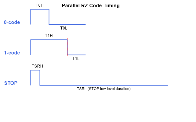
RZ Code API
Use the following interfaces to configure the high/low level durations of each symbol. Parameters are in pclk ticks:
void rz_set_t0h_t0l_time(unsigned short target_high_tick, unsigned short target_low_tick);
void rz_set_t1h_t1l_time(unsigned short target_high_tick, unsigned short target_low_tick);
void rz_set_tsrh_tsrl_time(unsigned short target_high_tick, unsigned short target_low_tick);
Timing calculation: n ticks correspond to n * 1000/sys_clk.pclk ns
For example, with PCLK = 24 MHz, 1 tick ≈ 41.67 ns:
rz_set_t0h_t0l_time(12, 33); // Code 0: 12*41.67≈500ns high level, 33*41.67≈1375ns low level
rz_set_t1h_t1l_time(23, 23); // Code 1: 23*41.67≈958ns high level, 23*41.67≈958ns low level
rz_set_tsrh_tsrl_time(0, 9000);// RESET code: 0ns high level, 9000*41.67≈375µs low level
Addressing Modes
Pixel ICs support two addressing modes:
- Serial sequential addressing: data is passed sequentially through serially connected pixel ICs
- Parallel random addressing: each pixel IC identifies its data by an address code, and all ICs share the same data line
Serial Sequential Addressing

As shown above, 3 pixel ICs work in series. D1 is the data sent by the RZ module, while D2, D3 and D4 are the return-to-zero data forwarded by the cascaded chips. Assuming each chip requires 24 bits of data, the RZ module sends multiple frame data, each frame containing 3 × 24-bit data, and a RESET code is sent immediately after each frame.
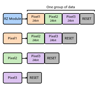
Parallel Random Addressing
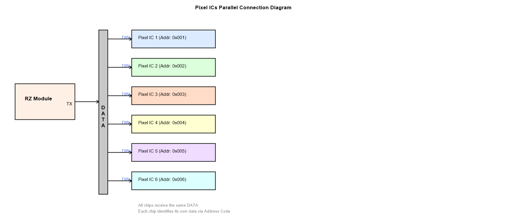
As shown above, 6 pixel ICs work in parallel, and all chips can receive the DATA sent by the RZ module. Each frame sent by the RZ module contains a Control Code, an Address Code, RGB data and a Stop Code. Each chip uses the Address Code to determine whether the current RGB data belongs to it.

Data Format Configuration
The data format of each pixel is controlled by the following parameters:
align_32bits_mode: data alignment (8-bit or 32-bit boundary)big_endian_mode: byte order (big-endian or little-endian)bit_msb: bit order (MSB or LSB first)global_data_mode: global data positionglobal_data_num: number of global data bits
void rz_set_pixel_ic_num(unsigned char pixel_ic_num) //Configure the number of pixels.
void rz_data_bit_num_per_pixel(unsigned char per_pixel_data) //Configure the number of bits per pixel.
For example, when the data is 0x12345678, the transmitted data under different configurations is as follows:
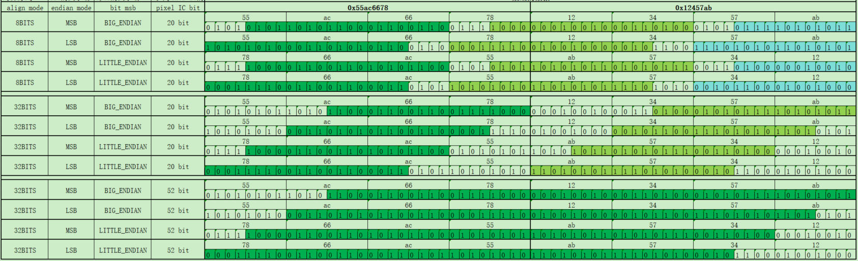
Note
-
If the data width is not a multiple of 8 bits/32 bits, padding data must be added to the array when using 8-bit/32-bit alignment mode. The padding data is not actually transmitted and is only used to satisfy the alignment requirement.**
-
The colored bits are the 20-bit/52-bit data actually sent out; the rest is padding data that is not transmitted.**
With global data (global_data_num = 1), the global data can be inserted in two ways:
global_data_mode = 0: the global data follows each pixel's dataglobal_data_mode = 1: the global data follows the data of all pixels
Features
Jitter
The RZ module supports the Jitter function, which can add random jitter to the low levels (T0L/T1L) and/or high levels (T0H/T1H) of code 0 and code 1 for EMC optimization.
The jitter amplitude is generated by a random number generator (PN module), and the jitter range is configured via the jitter_range parameter:
| jitter_range value | Jitter range (unit: Tpclk) |
|---|---|
| 0 | 0~1 |
| 1 | 0~3 |
| 2 | 0~7 |
| 3 | 0~15 |
| 4 | 0~31 |
| 5 | 0~63 |
| 6 | 0~127 |
| 7 | 0~255 |
Jitter enable control:
| Control bit | Description |
|---|---|
jitter_l_en |
Enable/disable Jitter on T0L and T1L |
jitter_h_en |
Enable/disable Jitter on T0H and T1H |
Output Polarity
| Polarity mode | Enum value | Description |
|---|---|---|
| Non-inverted | POLARITY_NO_INV |
Outputs high level during T0H/T1H and low level during T0L/T1L |
| Inverted | POLARITY_INV |
Outputs low level during T0H/T1H and high level during T0L/T1L |
FIFO and Interrupts
The RZ module contains an internal TX FIFO with the following status flags:
| Status flag | Enum value | Description |
|---|---|---|
| TX_BUF_CNT | FLD_RZ_TX_BUF_CNT |
Amount of data in the TX FIFO |
| TX_EMPTY | FLD_RZ_TX_EMPTY |
TX FIFO empty flag |
| TX_FULL | FLD_RZ_TX_FULL |
TX FIFO full flag |
| RZ_EN | FLD_RZ_EN |
RZ enable status |
FIFO API
unsigned char rz_get_txfifo_cnt(void); // Get the current data count in the TX FIFO
void rz_clr_txfifo_manual(void); // Manually clear the TX FIFO
void rz_clr_txfifo_auto(void); // Enable automatic TX FIFO clearing (already called inside rz_set_tx_config())
void rz_set_fifo_lvl(unsigned char fifo_lvl); // Set the FIFO threshold level (range 0~7, actual value = configured value + 1)
The FIFO watermark (fifo_lvl) is used to generate the int_lvl interrupt in MCU mode and the dma_req in DMA mode. The actual range of fifo_lvl is 1~8 and the configurable range is 0~7 (i.e. the configured value + 1 is the actual value), with a default value of 1.
Interrupt types and trigger conditions:
| Interrupt type | Enum value | Trigger condition | Clear method |
|---|---|---|---|
| FIFO watermark interrupt | FLD_RZ_CLR_INT_LVL |
Triggered when the number of bytes in the FIFO is less than fifo_lvl | Must be cleared manually |
| Transmission complete interrupt | FLD_RZ_CLR_INT_TXDONE |
Triggered when data transmission completes | Must be cleared manually |
| Error interrupt | FLD_RZ_CLR_INT_ERROR |
Triggered when the DMA response is not timely, causing an error | Must be cleared manually |
Note
The most commonly used interrupt is TXDONE (transmission complete), which notifies the CPU that the next DMA transfer can be started.
API
The core API is as follows:
void rz_set_tx_config(rz_tx_config_t *rz_tx_config)
Initialization of the RZ module is done via the rz_set_tx_config() function, which automatically performs the following operations: releases the RZ module from reset and enables the RZ module clock, configures output polarity/bit order/byte order/global data mode/data alignment/addressing mode, sets the FIFO watermark to the default value of 3, configures Jitter enable and range, and enables automatic TX FIFO clearing.
Typical Application
WS2811 is a commonly used LED driver IC that adopts single-wire return-to-zero code encoding. It is a typical application scenario of the RZ module's serial sequential addressing mode, and is the application given in the current driver example.
The WS2811 single-bit timing parameters are as follows:
| Parameter | Description | Typical value | Tolerance |
|---|---|---|---|
| T0H | Code 0, high level time | 0.5µs | ±150ns |
| T0L | Code 0, low level time | 2.0µs | ±150ns |
| T1H | Code 1, high level time | 2.0µs | ±150ns |
| T1L | Code 1, low level time | 0.5µs | ±150ns |
| RES | Reset code (per frame), low level time | ≥50µs | — |
Note
The table above shows the WS2811 high-speed mode parameters; in low-speed mode the typical values of T0H/T0L/T1H/T1L are doubled, while the RES code time remains unchanged.
WS2811 Protocol Characteristics
- Each LED node receives 24 bits of data (GRB order, 8 bits per color)
- 0 and 1 are distinguished by the duration of the high level
- Data is input via DIN and cascaded out via DOUT to the next chip
Example Code
/* DMA source buffer (must be 4-byte aligned) */
unsigned int g_ram_data_buffer[6] = {0x55ac6600, 0x000057ab, 0x00997f09,
0x80095512, 0x77990101, 0x00000000};
/* gpio config. */
gpio_function_dis(GPIO_PC0);
gpio_set_mux_function((gpio_func_pin_e)GPIO_PC0,RZ_TX);
/* rz protocol config. */
rz_tx_config_t rz_tx_config = {
.pola = POLARITY_NO_INV, // Output polarity, no inversion
.addr_mode = SERIAL_SEQUENTIAL_MODE, // Addressing mode: Series mode
.bit_msb = BIT_LSB, // Bit order: LSB priority
.big_endian_mode = BIG_ENDIAN_MODE, // Byte order: Big-endian
.global_data_mode = GLOBAL_DATA_AFTER_EACH_PIXEL_DATA, // Global data mode: After each pixel
.align_32bits_mode = EACH_PIXEL_DATA_AT_8BITS_BOUNDARY, // Data alignment: 8-bit alignment
.jitter_l_en = DISABLE_JITTER_ON_T0L_T1L, // T0L/T1L Jitter enable: Disabled
.jitter_h_en = DISABLE_JITTER_ON_T0H_T1H, // T0H/T1H Jitter enable: Disabled
.jitter_range = JITTER_RANGE_FROM_0_TO_1, // Jitter range: Invalid
};
rz_set_tx_config(&rz_tx_config);
rz_set_t0h_t0l_time(12, 33); // 0 code: 500 ns high level, 2000 ns low level
rz_set_t1h_t1l_time(23, 23); // 1 unit: 2000 ns high level, 500 ns low level
rz_set_tsrh_tsrl_time(0, 9000); // RESET code: 0ns high level, 50000us low level
rz_set_pixel_ic_num(8); // Number of LEDs = 8 Pixel ICs
rz_data_bit_num_per_pixel(24); // Each LED node receives 24-bit data (GRB sequence * 8 bits for each color)
/* dam config. */
delay_ms(20);
/* dam config. */
rz_set_dma_config(DMA1);
rz_set_dma(DMA1, (unsigned int*)(g_ram_data_buffer1), sizeof(g_ram_data_buffer1));
/* interrupt config. */
rz_set_irq_mask(FLD_RZ_MASK_TXDONE);
plic_interrupt_enable(IRQ_RZ);
core_interrupt_enable();
CAN
Concepts and Principles
Overview
The CAN (Controller Area Network) controller fully implements the CAN 2.0B and CAN FD protocols, complying with the ISO 11898-1 standard. Each channel can be independently configured as a CAN node or a CAN FD node.
Chips and channels that support CAN:
| Chip | CAN Channels |
|---|---|
| TL322X | CAN0, CAN1 |
| TL521X | CAN0 |
Key features:
- Supports Classical CAN 2.0A/B (standard frames with 11-bit ID, extended frames with 29-bit ID)
- Supports CAN FD (up to 64 data bytes, bit-rate switching BRS, rates up to 8Mbps)
- Up to 128 Message Buffers (MBs), each independently configurable as RX/TX
- Each MB has its own ID mask register (Individual Mask)
- Legacy Rx FIFO (stores up to 6 frames, Classical CAN only) and Enhanced Rx FIFO (stores up to 6 CAN FD frames), supporting DMA data transfer (single mode / linked-list mode)
- Legacy Rx FIFO ID filtering can match 128 extended IDs, 256 standard IDs, or 512 partial (8-bit) IDs, with up to 128 ID Filter Table elements
- Enhanced Rx FIFO ID filtering can match 64 extended-ID or 128 standard-ID filter elements, supporting three filtering schemes: mask + filter, range, and two filters without mask
- Self-test (Loopback), Listen-only, Self-Reception
- Remote frame support
- Error state machine (Error Active / Passive / Bus-Off)
- 16-bit free-running timer, with optional high-resolution 32-bit timer
- Low-power modes (Doze / Stop) and Pretended Networking (PN) wakeup
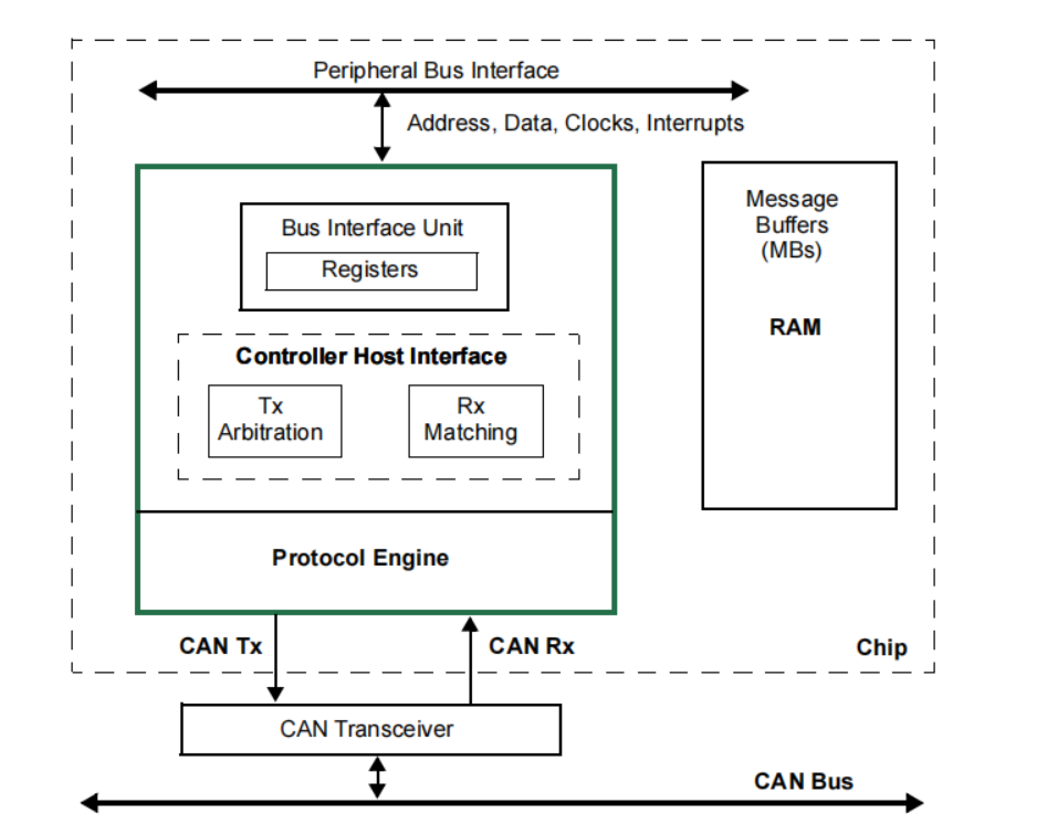
Operating Modes
| Mode | TX/RX Allowed | Key Config Changeable | Entry / Exit | Purpose |
|---|---|---|---|---|
| Normal | ✅ TX and RX | ❌ | Default state | Normal operation |
| Freeze | ❌ RX ignored | ✅ | can_enter_freeze_mode() / can_exit_freeze_mode() |
Initialization, bit-timing change |
| Bus-Off | ❌ Off the bus | ❌ | Entered automatically when error counters fill; recovers after 128 occurrences (11 bits each) of recessive bits | Fault isolation |
| Listen-Only | Receive only, no ACK, no TX | ❌ | can_listen_only_enable() |
Sniffing/debugging without disturbing the bus |
| Loopback | TX internally tied to RX, never reaches the bus | ❌ | can_loop_back_enable() |
Self-test (brs=0 recommended) |
| Low-Power | Wakeable by frames; returns to operating mode after wakeup | Limited | can_enter_doze_mode() / can_enter_stop_mode() / PN |
Sleep power saving |
Hardware Connection
The CAN controller only provides TTL-level TX / RX pins and cannot be attached to the bus directly. An external CAN transceiver is required for level conversion and differential TX/RX:
%%{init: {"theme": "base", "themeVariables": {"primaryColor": "#ffffff", "primaryTextColor": "#1f2937", "primaryBorderColor": "#d1d5db", "lineColor": "#6b7280", "clusterBkg": "#ffffff", "clusterBorder": "#d1d5db", "titleColor": "#1f2937"}}}%%
flowchart LR
MCU["MCU<br/>CAN Controller"] -->|"TX / RX"| TCV["CAN Transceiver"] -->|"CANH / CANL"| BUS["CAN Bus"]- The controller's
TX/RXpins connect to the corresponding pins of the transceiver, and the transceiver converts the single-ended signal into theCANH/CANLdifferential signal onto the bus. - Both ends of the bus need one 120Ω termination resistor each (ISO 11898-2 standard, regardless of baud rate) for impedance matching and to eliminate signal reflections.
- Shielded twisted pair cable is recommended. Transmission distance depends on baud rate (the higher the baud rate, the shorter the reliable distance; rule of thumb: about 40m at 1Mbps, several km at low speeds).
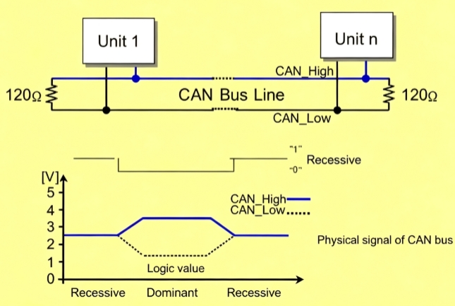
Reading Guide
- New to CAN: read "CAN Protocol Basics" first for background on frame types / frame formats / arbitration / bit stuffing.
- Only need to send and receive data: read "Usage Flow Overview" first for the overall sequence, then "Initialization and Configuration → Transmission / Reception" for details; for reception, pick one of the three options per your scenario (Rx MB / Legacy Rx FIFO / Enhanced Rx FIFO).
- Troubleshooting communication anomalies: read "Error Handling and Fault Confinement".
- Low-power / automotive wakeup scenarios: read "Low Power and Pretended Networking".
- Hands-on verification: get the corresponding mode running from "Demo" first, then adapt its source code to your application.
- Hardware wiring: see "Hardware Connection".
CAN Protocol Basics
This chapter covers only the protocol knowledge required to understand the driver, without register-related information. Readers already familiar with CAN can skip it.
(1) Frame Types
There are four frame types on a CAN bus:
| Frame Type | Purpose | Generated By |
|---|---|---|
| Data frame | Carries data; the most common type | Application layer (can_frame_t) |
| Remote frame | Requests "the data of a certain ID"; carries no data itself (RTR=1) | Application layer (can_frame_t) |
| Error frame | Sent automatically by the controller when a bus error is detected, notifying all nodes that the current transmission failed | Controller hardware, automatically |
| Overload frame | Inserts extra delay between consecutive frames; rarely seen in practice | Controller hardware, automatically |
Note
- The ID is a message identifier, not an address: CAN has no notion of "which one to send to". Every node on the bus receives every frame and uses the ID to decide whether to accept it. The ID in a remote frame therefore means "the data I am requesting"; the node responsible for producing that data responds when it sees the request.
(2) Classical CAN Frame Format
A frame is arranged on the wire in "sent first → sent later" order, so left to right is the transmission order (starting with SOF, ending with EOF):
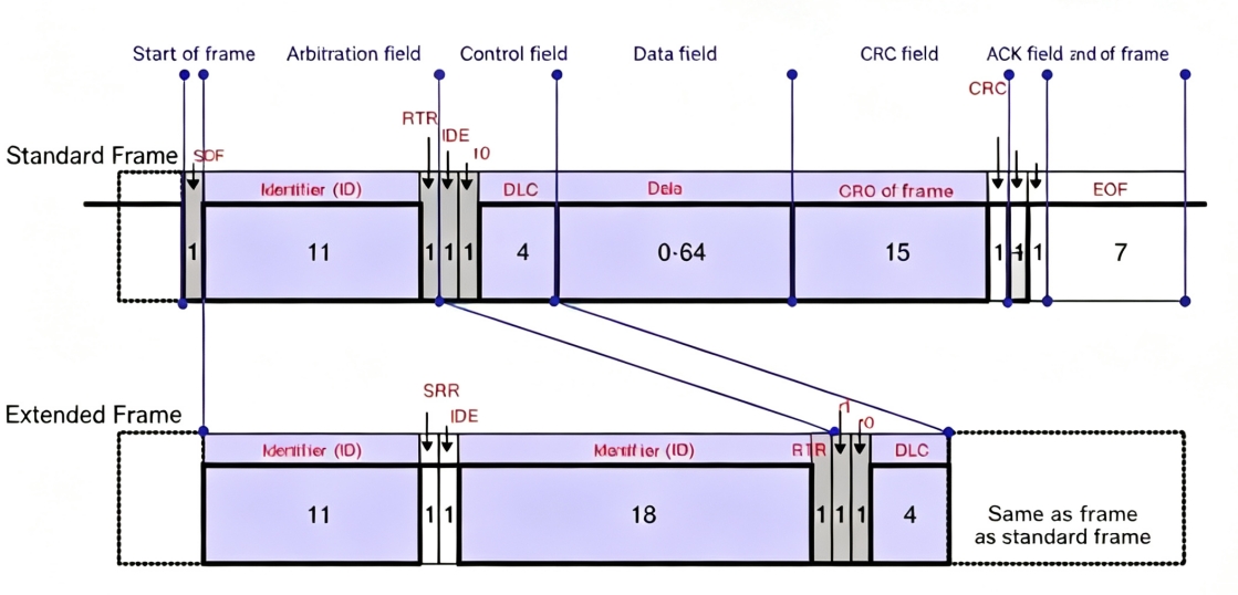
Field descriptions (using the standard 11-bit ID frame as an example):
| Field | Width | Description |
|---|---|---|
| SOF | 1 | Start of Frame, one dominant bit |
| ID | 11 / 29 | Arbitration field: 11-bit for standard frames, 29-bit for extended frames |
| RTR | 1 | Remote frame flag: 0 = data frame, 1 = remote frame |
| IDE | 1 | Extended frame flag: 0 = standard frame, 1 = extended frame |
| DLC | 4 | Data length code, 0–8 bytes |
| DATA | 0–64 bit | Data field, 0–8 bytes |
| CRC | 15 | Cyclic redundancy check |
| ACK | 2 | Acknowledgment field (ACK slot + delimiter) |
| EOF | 7 | End of frame, 7 recessive bits |
Note
- Compared with the standard frame, the extended frame (29-bit ID) adds SRR, an 18-bit extended ID, and R0/R1 reserved bits; these bits are handled by hardware and do not affect driver usage.
(3) CAN FD Frame Format
CAN FD frames are transmitted in the same order as classical frames. The differences are the three extra control bits EDL/BRS/ESI, the longer DLC/DATA/CRC, and no remote frame support:
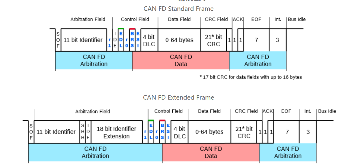
Field descriptions (in on-line order, matching the figure above):
| Field | Width | Description |
|---|---|---|
| SOF | 1 | Start of frame, one dominant bit |
| ID | 11 / 29 | Arbitration ID: 11-bit for standard frames, 29-bit for extended frames |
| IDE | 1 | Extended frame flag: 0 = standard frame, 1 = extended frame |
| EDL | 1 | Extended data length flag, distinguishes a CAN FD frame |
| BRS | 1 | Bit rate switching, whether the data segment switches to a higher baud rate |
| ESI | 1 | Error state indicator |
| DLC | 4 | Data length code, 0–64 bytes (non-linear encoding) |
| DATA | 0–512 bit | Data field, up to 64 bytes |
| CRC | 17 / 21 | Check (longer than classical) |
| ACK | 2 | Acknowledgment field (ACK slot + delimiter) |
| EOF | 7 | End of frame, 7 recessive bits |
Whether the data segment is accelerated is controlled by the BRS bit, used together with TDC. See "Bit Timing and Baud Rate" for details.
(4) Arbitration and Bit Stuffing
- Arbitration: this is the bus arbitration between nodes (defined by the CAN protocol) — when multiple nodes start transmitting while the bus is idle, they arbitrate bit by bit on the ID: the smaller the ID, the higher the priority (a dominant 0 overwrites a recessive 1). Nodes that lose arbitration automatically stop transmitting and switch to receiving. Which of the node's internal TX MBs goes first is a separate matter (local priority, inherent to the IP); see "Transmission · TX Arbitration".
- Bit stuffing: done automatically by controller hardware, no software involvement — on transmission, after every 5 consecutive bits of the same level an opposite-level bit is inserted; on reception, hardware removes it automatically. This guarantees synchronization and prevents desynchronization from long runs of identical levels. Bit stuffing happens only between SOF and the CRC sequence, excluding the CRC delimiter, ACK, and EOF.
Bit Timing and Baud Rate
(1) Time Quantum (Tq)
One CAN bit is internally processed as a number of "minimum time slices" called Tq (Time Quanta). Tq is obtained by prescaling the CAN module clock (PCLK):
Tq = 1 / ( PCLK / (presdiv + 1) )
= (presdiv + 1) / PCLK
presdiv: the prescaler field incan_timing_config_t; the actual division factor =presdiv + 1.PCLK: the CAN module input clock, derived from the system clock tree (i.e.,sys_clk.pclk); see the "Clock" chapter for its exact frequency.
One CAN bit consists of several consecutive Tq, whose duration is the single-bit time; the reciprocal of the bit time is the baud rate:
Bit Time = N_Tq × Tq
= N_Tq × (presdiv + 1) / PCLK
Bit Rate = 1 / Bit Time
= PCLK / [ (presdiv + 1) × N_Tq ]
So the baud rate is jointly determined by PCLK, presdiv, and N_Tq. Configuring a target baud rate is essentially finding a (presdiv, N_Tq) pair that satisfies the constraints.
One CAN bit is divided by purpose into four segments (all in units of Tq); N_Tq is the sum of the four:
| Segment | Purpose |
|---|---|
| SYNC_SEG | Synchronization segment, fixed at 1 Tq. Bus level transitions must occur inside this segment; used by all nodes for hard synchronization and to remove clock offset |
| PROP_SEG | Propagation segment, between the transmit point and the sample point, compensating for the physical delay of signal propagation on the bus plus the transceiver |
| PHASE_SEG1 | Phase buffer segment 1, absorbs clock deviations between nodes together with PHASE_SEG2 |
| PHASE_SEG2 | Phase buffer segment 2, absorbs clock deviations between nodes together with PHASE_SEG1 |
Two key time points in it:
- Transmit Point: the moment the node outputs a new bit level onto the bus, i.e., the start of the bit time.
- Sample Point: the moment the node samples the bus level and decides the bit value.
Following protocol grouping convention, PROP_SEG + PHASE_SEG1 together are called TSEG1, and PHASE_SEG2 is TSEG2, so:
N_Tq = 1 (SYNC_SEG) + PROP_SEG + PHASE_SEG1 + PHASE_SEG2
= 1 (SYNC_SEG) + TSEG1 + TSEG2
Note
- The four segments are the generic CAN protocol model. The SDK provides the three configuration fields
prop_seg/phase_seg1/phase_seg2. Note they hold "configuration values" — the actual Tq count = value + 1 (e.g.,prop_seg = 0means PROP_SEG is 1 Tq).
The sample point expresses "at what percentage position of the bit the level is read"; it is located at the end of PHASE_SEG1 / start of PHASE_SEG2, and is derived from the segments above, not measured value. Written as protocol formulas and substituting SDK fields, the second equation follows:
Sample Point(%) = (SYNC_SEG + TSEG1) / N_Tq × 100%
= (1 + PROP_SEG + PHASE_SEG1) / (1 + PROP_SEG + PHASE_SEG1 + PHASE_SEG2) × 100%
All nodes on the same bus must use the same baud rate, and sample points should be as close as possible (a deviation < 5% is recommended). For Classical CAN the sample point is recommended at 75%–87.5% (commonly 87.5%); CAN FD data segment bits are shorter, so the sample point usually moves earlier to 70%–80% (commonly 70%–75%, and as low as 60% at high bit rates).
Bit-time segmentation diagram (PCLK = 48MHz, 1Mbps, 16 Tq in total; sample point at the end of PHASE_SEG1 = 13/16 = 81.25%). Box widths are not to scale; the actual Tq count of each segment is labeled:
┌─────────┬──────────────┬──────────────────┬──────────────┐
│ SYNC_SEG│ PROP_SEG │ PHASE_SEG1 │ PHASE_SEG2 │
│ 1 Tq │ 4 Tq │ 8 Tq │ 3 Tq │
└─────────┴──────────────┴──────────────────┴──────────────┘
↑ ↑ ↑
TX Point Sample Point Next Bit TX Point
(81.25%)
The CAN FD data segment uses the same four-segment structure, only with a shorter bit time (fewer Tq per segment).
(2) Timing Configuration Structure
Bit timing is configured uniformly through the can_timing_config_t structure (field meanings are protocol-mode independent):
typedef struct {
// nominal segment (arbitration / Classical CAN)
volatile unsigned short presdiv; // Prescaler value; actual division = value + 1
volatile unsigned char phase_seg1; // Phase buffer segment 1 configuration value
volatile unsigned char phase_seg2; // Phase buffer segment 2 configuration value
volatile unsigned char prop_seg; // Propagation segment configuration value
volatile unsigned int nsjw; // Synchronization jump width
// data segment (CAN FD)
volatile unsigned short fd_presdiv;
volatile unsigned char fd_phase_seg1;
volatile unsigned char fd_phase_seg2;
volatile unsigned char fd_prop_seg;
volatile unsigned int dsjw;
volatile can_fd_protocol_timing_e canfd_timing_mode; // CANFD_FDCBT or CANFD_EDCBT
} can_timing_config_t;
These fields are usually filled automatically by can_cal_timing_config() / canfd_cal_timing_config() — you only supply the target baud rate and sample point. If you have already calculated the segment values manually per the tables above, you may also skip those APIs and fill can_timing_config_t directly.
(3) Synchronization Jump Width (SJW / RJW)
SJW (Sync Jump Width) defines by how many Tq a bit time may be lengthened or shortened at most during one resynchronization, absorbing the phase drift caused by crystal frequency deviations between nodes; its value does not exceed the smaller of PHASE_SEG1 and PHASE_SEG2. The current driver initializes it to 1 by default, adjustable through the can_timing_config_t definition.
(4) Classical CAN Timing
Field values and segment conversion for the Classical CAN bit timing:
| Parameter | Formula | Range | Description |
|---|---|---|---|
prop_seg |
PROP_SEG = value | 0–7 | Propagation segment |
phase_seg1 |
PHASE_SEG1 = value | 0–7 | Phase buffer segment 1 |
phase_seg2 |
PHASE_SEG2 = value | 0–7 | Phase buffer segment 2 |
presdiv |
Division factor = value + 1 | 0–255 | Prescaler |
| TSEG1 | = prop_seg + phase_seg1 + 2 |
2–16 Tq | Protocol grouping |
| TSEG2 | = phase_seg2 + 1 |
2–8 Tq | Protocol grouping |
| Total Tq per bit | = 1 + TSEG1 + TSEG2 | 8–25 | Recommended range |
The driver provides an automatic calculation API:
can_baud_rate_t rate_cfg={
.nominal_bit_rate = 1000000,
.nominal_sampling_rate = 0.8,
.nominal_sampling_rate_min=0.78,
.nominal_sampling_rate_max=0.82,
};
can_timing_config_t timing_cfg;
can_cal_timing_config(CAN0, &rate_cfg, sys_clk.pclk * 1000000, &timing_cfg);
// Parameters: channel, target baud rate (bps), PCLK (Hz), output structure, sample point (0.75 = 75%)
(5) CAN FD Timing
A CAN FD frame has two segements of bit-time, each with a different baud rate:
- Nominal segment (arbitration segment): multiple nodes contend for the bus together, at the nominal bit rate;
- Data segment: only one node is left transmitting and may speed up; with
brs=1it switches to the data bit rate.
Both baud rates are configured statically in one go at initialization through can_fd_baud_rate_t, and are not changed per frame at runtime.
For canfd_timing_mode fill CANFD_FDCBT or CANFD_EDCBT (use CANFD_FDCBT if unsure — the Demo default); the peer node may use a different mode, but the actual sample points must match.
Under both modes, field values and segment conversion for the nominal (arbitration) segment and the data segment (SYNC_SEG fixed at 1 Tq).
CANFD_FDCBT mode (default), nominal segment
| Parameter | Formula | Range | Description |
|---|---|---|---|
prop_seg |
EPROPSEG = value | 0–63 | Propagation segment |
phase_seg1 |
EPSEG1 = value | 0–31 | Phase buffer segment 1 |
phase_seg2 |
EPSEG2 = value | 0–31 | Phase buffer segment 2 |
presdiv |
EPRESDIV = value, division factor = value + 1 | 0–1023 | Prescaler |
| TSEG1 | = prop_seg + phase_seg1 + 2 |
2–96 Tq | Protocol grouping |
| TSEG2 | = phase_seg2 + 1 |
2–32 Tq | Protocol grouping |
| Total Tq per bit | = 1 + TSEG1 + TSEG2 | 8–129 | Recommended range |
CANFD_FDCBT mode (default), data segment
| Parameter | Formula | Range | Description |
|---|---|---|---|
fd_prop_seg |
FPROPSEG = value (no +1) | 0–31 | Propagation segment |
fd_phase_seg1 |
FPSEG1 = value | 0–7 | Phase buffer segment 1 |
fd_phase_seg2 |
FPSEG2 = value | 0–7 | Phase buffer segment 2 |
fd_presdiv |
FPRESDIV = value, division factor = value + 1 | 0–1023 | Prescaler |
| TSEG1 | = fd_prop_seg + fd_phase_seg1 + 1 |
2–39 Tq | Protocol grouping |
| TSEG2 | = fd_phase_seg2 + 1 |
2–8 Tq | Protocol grouping |
| Total Tq per bit | = 1 + TSEG1 + TSEG2 | 5–48 | Supports higher baud rates |
CANFD_EDCBT mode, nominal segment
| Parameter | Formula | Range | Description |
|---|---|---|---|
prop_seg + phase_seg1 |
Merged into NTSEG1 (incl. prop) = prop_seg + phase_seg1 (set fd_prop_seg to 0) |
0–255 | Phase buffer segment 1 (incl. propagation segment) |
phase_seg2 |
NTSEG2 = value | 0–127 | Phase buffer segment 2 |
presdiv |
Division factor = value + 1 | 0–1023 | Prescaler |
| TSEG1 | = ntseg1 + 1 (= prop_seg + phase_seg1 + 1) |
2–256 Tq | Protocol grouping |
| TSEG2 | = ntseg2 + 1 (= phase_seg2 + 1) |
2–128 Tq | Protocol grouping |
| Total Tq per bit | = 1 + TSEG1 + TSEG2 | 8–385 | Wider adjustment granularity |
CANFD_EDCBT mode, data segment
| Parameter | Formula | Range | Description |
|---|---|---|---|
fd_prop_seg + fd_phase_seg1 |
Merged into DTSEG1 (incl. prop) = fd_prop_seg + fd_phase_seg1 (set fd_prop_seg to 0) |
0–31 | Phase buffer segment 1 (incl. propagation segment) |
fd_phase_seg2 |
DTSEG2 = value | 0–15 | Phase buffer segment 2 |
fd_presdiv |
Division factor = value + 1 | 0–1023 | Prescaler |
| TSEG1 | = dtseg1 + 1 (= fd_prop_seg + fd_phase_seg1 + 1) |
2–32 Tq | Protocol grouping |
| TSEG2 | = dtseg2 + 1 (= fd_phase_seg2 + 1) |
2–16 Tq | Protocol grouping |
| Total Tq per bit | = 1 + TSEG1 + TSEG2 | 5–49 | Supports higher baud rates |
Automatic calculation API:
can_fd_baud_rate_t rate_cfg={
.canfd_timing_mode = CANFD_EDCBT,
.nominal_bit_rate = 1000000,
.nominal_sampling_rate = 0.8,
.nominal_sampling_rate_min=0.78,
.nominal_sampling_rate_max=0.82,
.data_bit_rate = 4000000,
.data_sampling_rate = 0.8,
.data_sampling_rate_min = 0.78,
.data_sampling_rate_max = 0.82,
};
can_timing_config_t timing_cfg;
canfd_cal_timing_config(CAN0, &rate_cfg, sys_clk.pclk * 1000000, &timing_cfg, 0.75);
Data segment bit-time diagram (PCLK = 48MHz, data segment 4Mbps, 12 Tq in total, sample point 75%; compared with the nominal segment's 48 Tq at 1Mbps, the data segment bit time is much shorter):
┌─────────┬──────────────┬──────────────────┬──────────────┐
│ SYNC_SEG│ PROP_SEG │ PHASE_SEG1 │ PHASE_SEG2 │
│ 1 Tq │ 3 Tq │ 5 Tq │ 3 Tq │
└─────────┴──────────────┴──────────────────┴──────────────┘
↑ ↑ ↑
TX Point Sample Point Next Bit TX Point
(75%)
Note
- The data segment baud rate applies only to FD frames with
edl=1andbrs=1; Classical CAN frames always use the nominal baud rate. A CAN FD node can also be used as a Classical CAN node.
TDC (Transmitter Delay Compensation)
- Problem: when the data segment rate is high (e.g., 2M–8M), the bit time is very short (only 125ns at 8M), while the transmitter's own delay (controller + transceiver loop, about 100–250ns) is already comparable to the bit time. The transmitting node would sample before the bit it sent actually reaches the bus, misjudging its own normal delay as a bit error.
- Solution: TDC shifts the data segment sample point back to a "Secondary Sample Point (SSP)", eliminating that misjudgment.
%%{init: {"theme": "base", "themeVariables": {"primaryColor": "#ffffff", "primaryTextColor": "#1f2937", "primaryBorderColor": "#d1d5db", "lineColor": "#6b7280", "clusterBkg": "#ffffff", "clusterBorder": "#d1d5db", "titleColor": "#1f2937"}}}%%
flowchart LR
A["TX sends the bit"] -->|"Loop delay td<br/>(approx. 100-250ns)"| B["Bit appears on the bus"]
B --> C["Transmitting node samples at SSP<br/>(SSP = SP + TDCO ≈ SP + td)"]Understand TDC on two levels:
- TDC enable (on/off): this driver enables TDC automatically in
canfd_init()whenbrs=1; there is no separate switch — passbrsas 0 to turn it off. This "TDC on whenever FD accelerates" policy is reasonable. - TDCO (compensation offset): this driver calculates TDCO automatically from the data segment bit-timing parameters and caps it at the register limit; a few scenarios such as non-standard transceivers or especially long cables may need a manual override. Use
canfd_set_tdcoto override the value manually.
Note
- Loopback mode: internal loopback does not pass through the transceiver; the loop delay ≈ 0, so no TDC compensation is needed. If TDC stays enabled, hardware re-samples according to the delay offset and may sample at the wrong position; therefore
brs=0is recommended for loopback testing.
Configuration Constraints
The automatic calculation APIs require an exact match:
- A configuration is returned only when
PCLKdivides the target baud rate evenly and a combination satisfying the sample-point constraints can be found; - Otherwise they return failure — no approximate baud rate with error is ever returned.
Therefore PCLK must be an integer multiple of the target baud rate (the actual frequency is decided by the system clock tree).
Baud-rate upper limits: nominal (arbitration) phase up to 1Mbps, data segment up to 8Mbps (chip capability; the practical limit depends on the transceiver and wiring).
Driver Usage
Note
- The code in this part shows key call snippets, focusing on APIs and parameters; business variables and macros such as
rx_frame,MB_RX_NUM,DMA_REV_LEN,TXMB_START_INDEXmust be defined with reference to the Demo (demo/vendor/CAN_Demo). See "Demo" for directly runnable examples.
Usage Flow Overview
The standard flow for using the CAN driver is as follows (step numbers match the chapters that follow):
%%{init: {"theme": "base", "themeVariables": {"primaryColor": "#ffffff", "primaryTextColor": "#1f2937", "primaryBorderColor": "#d1d5db", "lineColor": "#6b7280", "clusterBkg": "#ffffff", "clusterBorder": "#d1d5db", "titleColor": "#1f2937", "fontSize": "14px"}}}%%
flowchart TD
A["1. Pin + Module Enable"] --> B["2. Enter Freeze"]
B --> C["3. Calculate Bit Timing"]
C --> D["4. Configure MB + Init"]
D --> E["5. Configure TX"]
D --> F["6. Configure RX"]
E --> G["7. Exit Freeze"]
F --> G
G --> H["8. TX/RX"]
H -.-> I["9. Error Handling (Optional)"]
H -.-> J["10. Low Power / PN (Optional)"]Initialization and Configuration
(1) Freeze Mode
Enable the module before any configuration (must be called before other configurations):
can_set_pin(CAN0, CAN0_GPIO_TX_PIN, CAN0_GPIO_RX_PIN);
can_module_en(CAN0);
CAN is a continuous bit stream; changing key configurations such as bit timing during TX/RX disrupts the current frame, produces error frames, drives the error counters up, and in severe cases leads to Bus-Off. The controller therefore provides Freeze mode: first "lift" the controller off the bus (stop TX/RX and bit-time counting), change the key configuration, then exit Freeze to resume communication.
- Must be changed under Freeze: baud rate / sample point / SJW, CAN FD nominal and data segment bit times, TDC / TDCO, MB partitioning and filters / masks.
- During Freeze: no participation in bus communication — no frames are received or transmitted.
The driver wraps two APIs, which internally wait until the controller has actually entered/exited Freeze before returning:
can_enter_freeze_mode(): enter Freeze (call before starting to change configuration).can_exit_freeze_mode(): exit Freeze (call once after all configuration is done and before starting TX/RX).
Note
- Loopback is a self-test under normal mode: the transmit side is internally wired back to the receive side (not through the bus) to verify TX/RX without a peer node. It happens after exiting Freeze and is a different thing from Freeze, whose purpose is "lift off the bus to change configuration"; in the demo the two are written next to each other during initialization — do not confuse them.
(2) MB Partitioning (mb_cfg)
The MB (Message Buffer) is the carrier for TX and RX messages, analogous to a row of "mailboxes": to transmit, the CPU writes the message into a TX MB and hardware sends it; to receive, hardware writes matching messages into an RX MB for the CPU to read. The row of mailboxes is divided by index into a receive area and a transmit area, with the boundary defined by macros:
%%{init: {"theme": "base", "themeVariables": {"primaryColor": "#ffffff", "primaryTextColor": "#1f2937", "primaryBorderColor": "#d1d5db", "lineColor": "#6b7280", "clusterBkg": "#ffffff", "clusterBorder": "#d1d5db", "titleColor": "#1f2937"}}}%%
flowchart LR
MB0["MB0<br/>RX"] --> MB1["MB1<br/>RX"] --> MB2["MB2<br/>RX"] --> MB3["MB3<br/>RX"]
MB3 -->|"TX/RX boundary"| MB4["MB4<br/>TX"] --> MB5["MB5<br/>TX"] --> MB6["MB6<br/>TX"]##define RXMB_START_INDEX 0 // Index of the first RX MB
##define MB_RX_NUM 4 // Number of RX MBs
##define TXMB_START_INDEX 4 // Index of the first TX MB (= RXMB_START_INDEX + MB_RX_NUM)
Each MB always consists of 4-byte CS (control/status) + 4-byte ID + data area, and mb_data_size only changes the data-area size. can.h uses the union in mailbox_allocate_t to carve out different memory views per mb_data_size (with 16 / 32 / 64 bytes the MB RAM is split into 4 blocks):
typedef struct {
union {
// 8 bytes: 128 MBs, 16 bytes each (cs + id + 2 words)
struct { unsigned int cs; unsigned int id; unsigned int word[2]; } mb_8byte[128];
// 16 bytes: split into 4 blocks, 21 each, 84 in total
struct { struct { unsigned int cs; unsigned int id; unsigned int word[4]; } mb_16byte_0[21]; /* ..._1/_2/_3, 4 blocks */ } mb_16byte;
// 32 bytes: split into 4 blocks, 12 each, 48 in total
struct { struct { unsigned int cs; unsigned int id; unsigned int word[8]; } mb_32byte_0[12]; /* ..._1/_2/_3, 4 blocks */ } mb_32byte;
// 64 bytes: split into 4 blocks, 7 each, 28 in total
struct { struct { unsigned int cs; unsigned int id; unsigned int word[16]; } mb_64byte_0[7]; /* ..._1/_2/_3, 4 blocks */ } mb_64byte;
// Compatibility access view
struct { unsigned int cs; unsigned int id; unsigned int word0; unsigned int word1; } MB[127];
};
} mailbox_allocate_t;
CS key fields:
| Bits | Field | Description |
|---|---|---|
| [15:0] | TIME_STAMP |
Timestamp (written back by hardware on reception) |
| [19:16] | DLC |
Data length field value (Classical 0–8, FD 0–15 non-linear) |
| [20] | RTR |
Remote frame flag |
| [21] | IDE |
Extended frame flag |
| [22] | SRR |
Substitute remote request bit of extended frames |
| [27:24] | CODE |
MB status code (separate sets for RX / TX; see "Transmission" / "Reception") |
| [29] | ESI |
Error state indicator (CAN FD) |
| [30] | BRS |
Bit rate switching (CAN FD data segment acceleration) |
| [31] | EDL |
Extended data length (CAN FD frame flag) |
The CAN FD DLC field value maps to byte counts non-linearly (specified by ISO 11898-1, not specific to this chip):
- Field values 0–8 → 0–8 bytes;
- Field values 9–15 → 12 / 16 / 20 / 24 / 32 / 48 / 64 bytes respectively.
Distinguish "enum name" from "enum value":
- SDK enum names directly use byte counts, e.g.,
CAN_12B_PER_FRAMEmeans 12 bytes; - but the enum value equals the DLC field value —
CAN_12B_PER_FRAME= 0x9 — the two are not the same thing; - when reading a frame,
lengthholds the field value and must be converted to a byte count withDLC_LENGTH_DECODE(length).
All MBs share one fixed RAM block (128 × 16 = 2048 bytes), which hardware divides into 4 blocks of 512 bytes each. Each MB is always = 4-byte CS + 4-byte ID + mb_data_size data, so:
- One MB footprint = 4 + 4 +
mb_data_size; - Each block fits
512 ÷ per-MB footprintMBs (rounded down; an MB cannot straddle blocks); - Total MB count = per-block count × 4.
mb_data_size |
Per-MB data | Per-MB footprint (CS+ID+data) | MBs per block | Total MBs |
|---|---|---|---|---|
CAN_8BYTE_PERMB |
8 bytes | 16 bytes | 32 | 128 |
CAN_16BYTE_PERMB |
16 bytes | 24 bytes | 21 | 84 |
CAN_32BYTE_PERMB |
32 bytes | 40 bytes | 12 | 48 |
CAN_64BYTE_PERMB |
64 bytes | 72 bytes | 7 | 28 |
Example: with 16-byte data, one MB takes 24 bytes; each block fits 512 ÷ 24 = 21.3 → 21 MBs, 4 blocks give 84 in total (8 bytes remain per block — not enough for a 22nd).
can_mb_cfg_t mb_cfg = {
.mb_max = 16, // Number of MBs actually enabled (≤ the totals above)
.mb_data_size = CAN_8BYTE_PERMB // Data-area size of each MB
};
mb_max decides how many MBs are actually enabled, and mb_data_size decides each MB's data-area size. How large mb_max should be depends on how many MBs TX uses + which reception method RX uses (the three consume MBs differently):
| Reception method | Does the FIFO consume MBs | Note |
|---|---|---|
| Rx MB | No | Each MB binds one ID |
| Legacy Rx FIFO | Yes | Takes MB0–MB5 + the filter table; CAN_8BYTE_PERMB required |
| Enhanced Rx FIFO | No | Uses independent RAM, consumes no MBs; CAN FD friendly |
See "Transmission" (TX MB) and "Reception" (the three reception methods) for how to configure each. Switching mb_data_size changes the whole MB memory layout and must be configured inside Freeze (can_init() / canfd_init() handle this internally).
At the software level, MBs are actually read/written through the frame structures can_frame_t / can_fd_frame_t, whose fields correspond one-to-one with the MB's CS / ID / DATA. See "Frame Structure".
(3) can_init / canfd_init
Two initialization APIs; canfd_init has one more parameter, brs, than can_init:
void can_init(can_chn_e chn, can_timing_config_t *timing_config, can_mb_cfg_t *mb_cfg,
unsigned char irmq_en, unsigned char tx_is_lprio_en);
void canfd_init(can_chn_e chn, can_timing_config_t *timing_config, can_mb_cfg_t *mb_cfg,
unsigned char brs, unsigned char irmq_en, unsigned char tx_is_lprio_en);
Parameters:
chn: channel,CAN0/CAN1.timing_config: bit timing (baud rate / sample point), computed bycan_cal_timing_config(); see "Bit Timing and Baud Rate" for details.mb_cfg: MB count and data width, fill{ .mb_max, .mb_data_size }; see "MB Partitioning (mb_cfg)" above.irmq_en: RX mask mode,1individual masks /0global mask; usually1.tx_is_lprio_en: TX arbitration,0lower-numbered MB first /1higher-priority first.brs(canfd_initonly): data segment acceleration,1on (TDC enabled automatically) /0off.
can_init(CAN0, &timing_cfg, &mb_cfg, 1, 0); // Classical CAN
canfd_init(CAN0, &timing_cfg, &mb_cfg, 1, 1, 0); // CAN FD, brs=1 data segment acceleration
After initialization the controller is in normal TX/RX mode; the three special modes below are off by default and enabled on demand:
- Self-reception:
can_self_reception_enable()— allows receiving frames sent by this node itself (self-reception disabled by default). - Listen-only:
can_listen_only_enable()— listen to the bus without transmitting / acknowledging / arbitrating, for bus monitoring and diagnosis. - Loopback:
can_loop_back_enable()— TX internally tied to RX, bypassing the transceiver and the bus, for single-board self-testing; self-reception must also be enabled to read loopback data (see Demoapp_loopback.cfor a complete example).
Note
- Classical CAN samples three points by default; CAN FD uses a fixed single sample point.
Frame Structure
When actually reading/writing MBs, the software layer uses "frame structures" whose fields correspond one-to-one with the MB's CS / ID / DATA. TX and RX use the same structure — there is no separate "TX frame / RX frame": when transmitting the CPU fills it, when receiving hardware fills it (the CPU reads it). The driver provides different frame structures for Classical CAN and CAN FD, both organizing data in big-endian order (big-endian transmission by default).
The type field distinguishes data frames / remote frames (see the frame types in "CAN Protocol Basics"); error frames and overload frames are handled automatically by hardware and need no software configuration.
Classical CAN frame can_frame_t (from can.h):
typedef struct {
struct { // Word 1: control and status (bit fields)
unsigned int timestamp : 16; // Timestamp
unsigned int length : 4; // Data length 0–8
unsigned int type : 1; // CAN_FRAME_TYPE_DATA / REMOTE
unsigned int format : 1; // CAN_FRAME_FORMAT_STANDARD / EXTEND
unsigned int : 1; // Reserved
unsigned int idhit : 9; // Rx FIFO filter hit ID (FIFO reception mode only)
};
struct { // Word 2: ID and priority (bit fields)
unsigned int id : 29; // Frame ID, generated with CAN_ID_STD() / CAN_ID_EXT()
unsigned int prio : 3; // TX local priority
};
union { // Data area: 8 bytes, two views of the same memory
struct { unsigned int data_word0;
unsigned int data_word1; };
struct { unsigned char data_byte0; // data_byte0 to data_byte7
/* ... */ };
};
} can_frame_t;
The CAN FD frame can_fd_frame_t adds FD-related bits and a larger data area on this basis:
typedef struct {
struct {
unsigned int timestamp : 16;
unsigned int length : 4; // DLC; convert to byte count with DLC_LENGTH_DECODE()
unsigned int type : 1;
unsigned int format : 1;
unsigned int srr : 1; // ← new
unsigned int : 6; // Reserved
unsigned int esi : 1; // ← new
unsigned int brs : 1; // ← new
unsigned int edl : 1; // ← new
};
struct { unsigned int id : 29;
unsigned int prio : 3; };
union {
struct { unsigned int data_word[16]; }; // Up to 64 bytes
struct { unsigned char data_byte0; /* ... */ };
};
unsigned int idhit; // ← new, Enhanced Rx FIFO filter hit ID
unsigned int hr_time_stamp; // ← new, high-resolution timestamp
} can_fd_frame_t;
Note
- The offset of
idhitinside the CAN FD frame structure varies dynamically with the DLC; after DMA reception, callcan_enhanced_rxfifo_dma_reset_idhit()to relocate it (see the "Enhanced Rx FIFO" chapter).
The data area offers both a data_word (32-bit word) view and a data_byte (byte) view of the same memory. The bus is big-endian: within each word the high byte goes first and words are in order, so data_byte0 is the lowest byte of the word (the last one received); the total data length need not be a multiple of 4 — it is decided by the DLC, and if fewer than 4 bytes, only the high-order bytes of the word are sent. For how to fill and read during TX / RX, see "Transmission" and "Reception".
Transmission
Transmission can only be done through MBs; there is no independent DMA transmit mode. Write the data into an MB and activate the CS CODE, and hardware transmits automatically. Before transmitting, configure the MB as TX with can_set_tx_mailbox_cfg() / canfd_set_tx_mailbox_cfg() (usually done once during initialization). The simplest usage is one TX MB: wait for the previous frame to finish before writing the next.
Transmission flow:
%%{init: {"theme": "base", "themeVariables": {"primaryColor": "#ffffff", "primaryTextColor": "#1f2937", "primaryBorderColor": "#d1d5db", "lineColor": "#6b7280", "clusterBkg": "#ffffff", "clusterBorder": "#d1d5db", "titleColor": "#1f2937"}}}%%
flowchart LR
A["Fill Frame<br/>can_frame_t / can_fd_frame_t"] --> B["Write & Activate TX MB<br/>can_write_tx_mb / canfd_write_tx_mb"]
B --> C["HW Arbitration by Priority<br/>tx_is_lprio_en"]
C --> D["Transmit after winning the bus"]
D --> E["CODE auto-returns to INACTIVE<br/>Ready for next frame"]can_write_tx_mb() / canfd_write_tx_mb() set the MB's CODE to active (TX_DATA) after writing; hardware transmits after winning arbitration, and CODE automatically returns to INACTIVE when done, so the MB can be written again.
(1) CAN Transmission
// 1) Configure this MB as TX first (usually done once during initialization; afterwards only the MB write is needed per frame)
can_set_tx_mailbox_cfg(CAN0, TXMB_START_INDEX, 1); // chn, MB index, 1 = enable
// 2) Fill the frame
can_frame_t tx_frame;
tx_frame.id = CAN_ID_STD(0x123);
tx_frame.format = CAN_FRAME_FORMAT_STANDARD;
tx_frame.type = CAN_FRAME_TYPE_DATA;
tx_frame.length = 8;
tx_frame.data_word0 = 0x00112233;
tx_frame.data_word1 = 0x44556677;
// 3) Write and send
can_write_tx_mb(CAN0, TXMB_START_INDEX, &tx_frame, 0);
// Last parameter: 0 = normal transmission, 1 = remote frame reply
(2) CAN FD Transmission
can_fd_frame_t tx_fd_frame;
tx_fd_frame.id = CAN_ID_STD(0x123);
tx_fd_frame.format = CAN_FRAME_FORMAT_STANDARD;
tx_fd_frame.type = CAN_FRAME_TYPE_DATA;
tx_fd_frame.length = CAN_16B_PER_FRAME; // DLC enum
tx_fd_frame.edl = 1; // Extended data length
tx_fd_frame.brs = 1; // Bit rate switching
for (unsigned char i = 0; i < DLC_LENGTH_DECODE(CAN_16B_PER_FRAME); i++) {
((unsigned char *)tx_fd_frame.data_word)[i] = g_tx_buff[i];
}
canfd_write_tx_mb(CAN0, TXMB_START_INDEX, &tx_fd_frame);
Note
- Whether this frame switches to the data segment high rate is decided by the MB's CS control fields:
edl=1marks it as an FD frame, and only withbrs=1does the data segment switch baud rate; both are set independently per frame.
(3) Data Filling and Byte Order
Transmitted data is big-endian by default: within each word the high byte goes first, words in order. Two ways to fill:
- The data is already a word value (high byte first): direct assignment is easiest:
data_word0 = 0x00112233→ the bus sends00 11 22 33in sequence. - The data is a byte array to be sent in array order: copying bytes directly on a little-endian machine reverses the order; use
data_convert_by_word()to reverse by word:
for (unsigned char j = 0; j < DLC_LENGTH_DECODE(CAN_8B_PER_FRAME); j++) {
*(((unsigned char *)&tx_frame.data_word0) + j) = g_tx_buff[j];
}
data_convert_by_word((unsigned char *)&tx_frame.data_word0, DLC_LENGTH_DECODE(CAN_8B_PER_FRAME));
data_convert_by_word() reverses byte order in units of 4 bytes (word); a tail shorter than 4 bytes is reversed as well. The Demo (app_tx_mode.c) uses the IS_LITTLE_END_CONVERT macro to control whether to convert, default 0 (no conversion).
Note
- The total data length is decided by the DLC and need not be a multiple of 4: with
length = 3anddata_word0 = 0x00112233, only the high 3 bytes00 11 22are sent (the low byte0x33is ignored).
(4) TX Completion Detection
- Interrupt method:
can_set_mb_irq_mask(CAN0, TXMB_START_INDEX)enables the corresponding TX MB interrupt; query that MB's interrupt flag in the ISR; - Polling method: query
can_get_mb_irq_status(), or check the MB's CSCODEfield.
TX MB CODE status codes:
| Status Code | Value | Meaning |
|---|---|---|
CAN_TX_MB_INACTIVE |
0x8 | Inactive / transmission complete, can be rewritten |
CAN_TX_MB_ABORT |
0x9 | Aborted |
CAN_TX_MB_DATA_OR_REMOTE |
0xc | Written, waiting for arbitration to transmit |
CAN_TX_MB_TANSWER |
0xe | Remote reply frame |
(5) TX Arbitration
When multiple TX MBs inside a node are ready, which one transmits first is decided by the tx_is_lprio_en parameter of can_init() / canfd_init(). This is the IP's inherent local priority mechanism, on a different level from bus ID arbitration — first an MB is selected inside the node, then arbitration by ID happens on the bus:
tx_is_lprio_en |
Arbitration |
|---|---|
| 1 | Local priority enabled (LPRIO_EN); the higher-priority MB transmits first |
| 0 | Arbitration by MB index; the lowest-index MB transmits first |
Reception
CAN is a broadcast bus: once a frame arrives, the controller filters it by ID to decide where it goes. The three reception methods are not "serial" — one frame ends up in exactly one place:
%%{init: {"theme": "base", "themeVariables": {"primaryColor": "#ffffff", "primaryTextColor": "#1f2937", "primaryBorderColor": "#d1d5db", "lineColor": "#6b7280", "clusterBkg": "#ffffff", "clusterBorder": "#d1d5db", "titleColor": "#1f2937"}}}%%
flowchart LR
BUS["Frame on the bus"] --> IDCHK{"Controller filters by ID<br/>(priority decides which is checked first)"}
IDCHK -->|"Match a Rx MB"| MB["Corresponding Rx MB"]
IDCHK -->|"Match FIFO filter table"| FIFO["Legacy / Enhanced Rx FIFO"]
IDCHK -->|"No match"| DROP["Drop"]Which one is checked first is decided by the reception priority priority. It is a field of the FIFO configuration structure (can_rx_fifo_config_t for Legacy / can_enhanced_rx_fifo_config_t for Enhanced), of type can_rx_fifo_priority_t, set together with the configuration in can_set_legacy_rxfifo_cfg() / can_set_enhanced_rxfifo_cfg():
CAN_RXFIFO_PRIO_HIGH(0x1): check the FIFO first;CAN_RXFIFO_PRIO_LOW(0x0): check the Rx MB first.
| Legacy FIFO enabled | irmq_en |
Priority | Rx MB status | Legacy FIFO status | Reception result |
|---|---|---|---|---|---|
| 1 | 1 | 0 | X | Not full | FIFO |
| 1 | 1 | 0 | None | Full | None |
| 1 | 1 | 0 | Free | Full | First MB |
| 1 | 1 | 0 | Not free | Full | Last MB |
| 1 | 1 | 1 | None | NotFull | FIFO |
| 1 | 1 | 1 | Free | X | First MB |
| 1 | 1 | 1 | Not free | NotFull | FIFO |
| 1 | 1 | 1 | Not free | Full | Last MB |
(2) Comparison of the Three Reception Modes
| Mode | CAN | CAN FD | Filtering Capability | MB Usage | DMA |
|---|---|---|---|---|---|
| Rx MB | ✅ | ✅ | 1 ID / MB | 1 per MB | ❌ |
| Legacy Rx FIFO | ✅ | ❌ | Up to 128 elements | 6 + filter table | ✅ |
| Enhanced Rx FIFO | ✅ | ✅ | Up to 128 pairs | None | ✅ |
Note
- Legacy Rx FIFO and Enhanced Rx FIFO cannot be enabled at the same time.
(2) Rx MB Mode
Each MB binds one ID filter, suitable when there are few IDs and sources must be strictly distinguished. After reception the CPU must read the MB promptly; otherwise the next frame with the same ID overwrites it (OVERRUN).
The driver wraps the standard flow for reading an Rx MB:
- Read the CS field (locks the MB);
- Read the ID, data, and other contents;
- Read the free-running timer (unlocks the MB).
Two additional notes:
- Before unlocking, if another frame with the same ID arrives, its data is held in an internal buffer and written into the MB only after it is unlocked;
- Rx MB has no FIFO mechanism. To emulate a FIFO with multiple Rx MBs, configure them with the same filter ID and sort by timestamp — only then is ordered reception guaranteed.
Configuring filtering requires two APIs together:
can_set_rx_mailbox_cfg(chn, mb_index, &cfg, enable): configures the ID, frame format, and frame type this MB matches, and activates it as an RX MB;can_set_rx_individual_mask(chn, mask_index, &mask): configures this MB's individual mask, deciding which ID bits participate in matching (requirescan_initwithirmq_en = 1).
How to fill the parameters:
cfg.id: the target ID to match, generated withCAN_ID_STD(id)(standard 11-bit) /CAN_ID_EXT(id)(extended 29-bit); do not write raw values;cfg.format/cfg.type:CAN_FRAME_FORMAT_STANDARD/EXTEND,CAN_FRAME_TYPE_DATA/REMOTE;cfg.remote_type: remote frame handling; fillNONEfor data frames;mask: generated withCAN_RX_MB_STD_MASK(id, rtr, ide); the first parameteridis "the bits that participate in matching" (a bit participates in comparison only when it is 1):0x7ff: all 11 bits participate → exact match of a single standard ID;0xff: only the low 8 bits participate → matches a group of IDs "with identical low 8 bits";0: none participate → any ID is received.
For example, "receive only standard data frames with ID = 0x123" → id = CAN_ID_STD(0x123), mask = CAN_RX_MB_STD_MASK(0x7ff, 0, 0); "receive a group of frames whose low 8 bits are 0 (0x000, 0x100, 0x200…)" → id = CAN_ID_STD(0x00), mask = CAN_RX_MB_STD_MASK(0xff, 0, 0).
can_rx_mb_config_t rxmb_cfg[4] = {
// id (target ID), frame format, frame type, remote frame handling
{CAN_ID_STD(0x00), CAN_FRAME_FORMAT_STANDARD, CAN_FRAME_TYPE_DATA, NONE},
{CAN_ID_STD(0x01), CAN_FRAME_FORMAT_STANDARD, CAN_FRAME_TYPE_DATA, NONE},
{CAN_ID_STD(0x02), CAN_FRAME_FORMAT_STANDARD, CAN_FRAME_TYPE_DATA, NONE},
{CAN_ID_STD(0x03), CAN_FRAME_FORMAT_STANDARD, CAN_FRAME_TYPE_DATA, NONE},
};
unsigned int rxmb_individual_mask[4] = {
CAN_RX_MB_STD_MASK(0xff, 0, 0), // 0xff: low 8 bits participate in matching (high bits ignored)
CAN_RX_MB_STD_MASK(0xff, 0, 0),
CAN_RX_MB_STD_MASK(0xff, 0, 0),
CAN_RX_MB_STD_MASK(0xff, 0, 0),
};
for (unsigned char i = 0; i < 4; i++) {
can_set_rx_mailbox_cfg(CAN0, i, &rxmb_cfg[i], 1); // Configure ID + activate the RX MB
can_set_rx_individual_mask(CAN0, i, &rxmb_individual_mask[i]); // Configure the individual mask
}
Note
- Mask semantics: after a frame arrives, hardware only checks "the ID bits whose mask is 1"; those bits must equal the corresponding bits of
cfg.idfor the frame to be stored into that MB; bits whose mask is 0 are ignored. So the 4 MBs above receive all standard frames whose "low 8 bits = 0x00 / 0x01 / 0x02 / 0x03" respectively.
Interrupt reception: first enable the MB's interrupt with can_set_mb_irq_mask(CAN0, mb_index), then query that MB's interrupt flag in the ISR:
_attribute_ram_code_sec_ void can0_irq_handler(void) {
for (unsigned char i = 0; i < MB_RX_NUM; i++) {
if (can_get_mb_irq_status(CAN0, i)) {
can_read_rx_mb(CAN0, i, &rx_frame[i]);
can_clr_mb_irq_status(CAN0, i);
break;
}
}
}
Note
- To detect reception completion, poll the interrupt flag, not the CODE field.
Read-back data is likewise big-endian: data_word0 = 0x00112233 means the bus received 00 11 22 33 in order, and the byte view data_byte0 = 0x33 (the word's lowest byte, i.e., the byte received last). If the application needs little-endian values, call data_convert_by_word() after reading back.
RX MB CODE status codes:
| Status Code | Value | Meaning |
|---|---|---|
CAN_RX_MB_INACTIVE |
0x0 | Inactive |
CAN_RX_MB_EMPTY |
0x4 | Activated and empty, waiting for reception |
CAN_RX_MB_FULL |
0x2 | Full, waiting for the CPU to read |
CAN_RX_MB_OVERRUN |
0x6 | Overwritten while full |
CAN_RX_MB_BUSY |
0x8 | Hardware is writing; not accessible by the CPU |
CAN_RX_MB_RANSWER |
0xa | Remote request received, auto reply configured |
(3) Legacy Rx FIFO Mode
The Legacy Rx FIFO lets hardware store matching frames into the FIFO in order, so the CPU does not have to read them immediately. It supports Classical CAN only and buffers at most 6 frames.
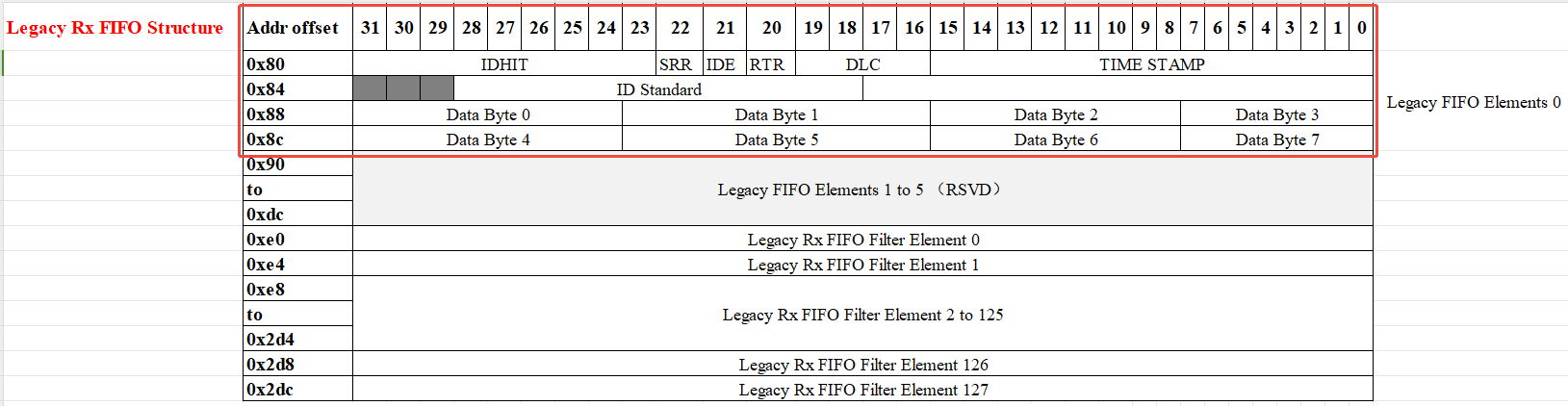
Filter Types
| Type | IDs per Element | Matching Capability |
|---|---|---|
CAN_RXFIFO_FILTER_TYPE_A |
1 | Full ID (11/29-bit) |
CAN_RXFIFO_FILTER_TYPE_B |
2 | Full standard ID / partial 14-bit extended ID |
CAN_RXFIFO_FILTER_TYPE_C |
4 | Partial 8-bit |
The corresponding filter macros are in can.h (CAN_RX_FIFO_STD_FILTER_TYPE_A etc.); the mask macros are CAN_RX_FIFO_STD_MASK_TYPE_A etc.
The filter table is fixed by hardware at at most 128 elements (id_filter_num cannot exceed this).
Number of MBs Occupied by the FIFO
The Legacy Rx FIFO has no independent RAM and occupies the front part of the MB RAM:
- MB0–MB5: the 6-frame FIFO buffer;
- From MB6: the filter table.
Total MBs occupied = 6 + (rffn + 1) × 2, where rffn is the smallest value satisfying 8 × (rffn + 1) ≥ id_filter_num, calculated automatically inside can_set_legacy_rxfifo_cfg(). For example, 4 TYPE_A filter elements → rffn = 0 → occupies 6 + 2 = 8 MBs (MB0–MB7).
In this case mb_data_size must be CAN_8BYTE_PERMB, and the MBs occupied by the FIFO must be deducted from mb_max; only the remaining MBs are usable for RX/TX.
Configuration Example
The configuration API is can_set_legacy_rxfifo_cfg(chn, &cfg, enable); the fields of can_rx_fifo_config_t:
id_filter_table: the filter table array, each element generated with theCAN_RX_FIFO_STD_FILTER_TYPE_x(id, rtr, ide)/..._EXT_...macros;id_filter_type: TYPE_A/B/C, deciding how many IDs each element matches (see table above);id_filter_num: the number of filter elements (≤ 128);priority: check the FIFO or Rx MBs first.
Masks are still configured separately with can_set_rx_individual_mask(); the 0x7ff in CAN_RX_FIFO_STD_MASK_TYPE_A(0x7ff, 0, 0) means all 11 bits participate in matching (exact match of a single ID).
##define FILTER_CNT 4
can_rx_fifo_config_t rxfifo_config;
unsigned int rxfifo_id_filter[FILTER_CNT] = {
CAN_RX_FIFO_STD_FILTER_TYPE_A(0x00, 0, 0),
CAN_RX_FIFO_STD_FILTER_TYPE_A(0x01, 0, 0),
CAN_RX_FIFO_STD_FILTER_TYPE_A(0x02, 0, 0),
CAN_RX_FIFO_STD_FILTER_TYPE_A(0x03, 0, 0),
};
unsigned int rxfifo_individual_mask[FILTER_CNT] = {
CAN_RX_FIFO_STD_MASK_TYPE_A(0x7ff, 0, 0),
CAN_RX_FIFO_STD_MASK_TYPE_A(0x7ff, 0, 0),
CAN_RX_FIFO_STD_MASK_TYPE_A(0x7ff, 0, 0),
CAN_RX_FIFO_STD_MASK_TYPE_A(0x7ff, 0, 0),
};
rxfifo_config.id_filter_table = rxfifo_id_filter;
rxfifo_config.id_filter_type = CAN_RXFIFO_FILTER_TYPE_A;
rxfifo_config.id_filter_num = FILTER_CNT;
rxfifo_config.priority = CAN_RXFIFO_PRIO_HIGH;
can_set_legacy_rxfifo_cfg(CAN0, &rxfifo_config, 1);
for (unsigned char i = 0; i < FILTER_CNT; i++) {
can_set_rx_individual_mask(CAN0, i, &rxfifo_individual_mask[i]);
}
Interrupt Reception
Enable the FIFO available interrupt, which fires whenever there is data in the FIFO:
can_set_legacy_rxfifo_irq_mask(CAN0, CAN_LEGACY_RXFIFO_AVAILD_IRQ);
In the ISR, read the FIFO head address directly; no read/write pointers need to be maintained (handled by hardware automatically):
_attribute_ram_code_sec_ void can0_irq_handler(void) {
if (can_get_legacy_rxfifo_irq_status(CAN0, CAN_LEGACY_RXFIFO_AVAILD_IRQ)) {
can_read_legacy_rxfifo(CAN0, &rx_frame[rx_done]);
can_clr_legacy_rxfifo_irq_status(CAN0, CAN_LEGACY_RXFIFO_AVAILD_IRQ);
}
}
DMA Reception / Linked List
DMA transfer is configured the same way as for the Enhanced Rx FIFO; the differences and common code are described in "DMA Reception (Common to Legacy / Enhanced)" below. Legacy-specific note: the first 4 bytes of the receive buffer are used by hardware to write back the length, so the data address should be buffer start + 4.
(4) Enhanced Rx FIFO Mode
Characteristics of the Enhanced Rx FIFO:
- Supports CAN / CAN FD frames, with data up to 64 bytes;
- Up to 128 pairs of filter elements;
- Consumes no MB RAM (uses independent RAM);
- Supports watermark triggering: the interrupt / DMA fire only after N frames have accumulated.
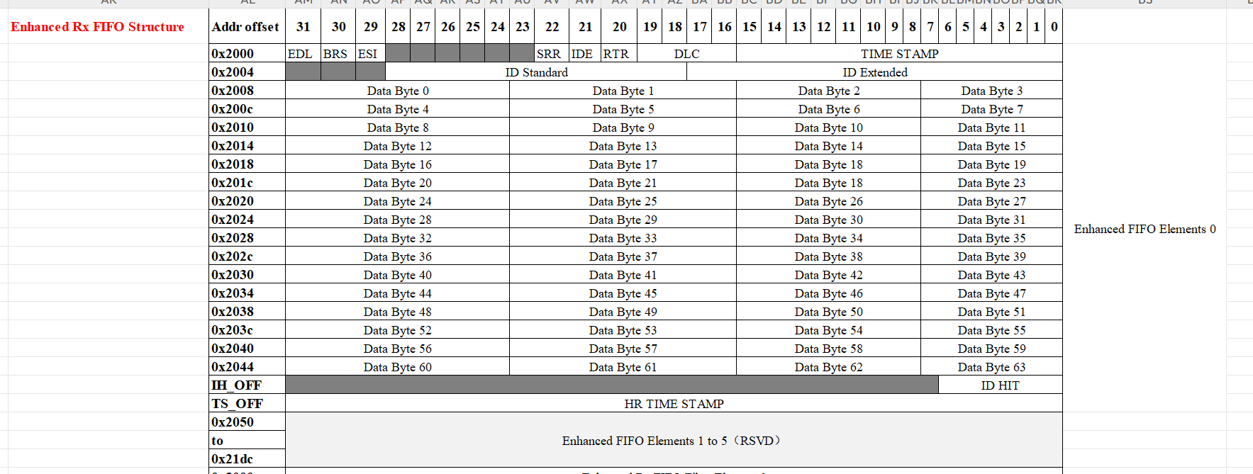
Filter Element Format
| FSCH | Mode | Description |
|---|---|---|
| 00 | Mask + Filter | ID + mask matching |
| 01 | Range | ID range [lower, upper] |
| 10 | Two Filters | Exact match of two IDs |
An extended-ID element takes 2 words, a standard-ID element 1 word, and extended-ID elements must be placed at the front of the filter table. The driver provides the corresponding macros (CAN_ENHANCED_RX_FIFO_EXT_TWO_FILTERS_LOW/HIGH etc.).
A "pair" is one filter rule combining mask + filter; the filter table is fixed by hardware at at most 128 pairs (id_filter_pairnum cannot exceed this).
Configuration Example
The configuration API is can_set_enhanced_rxfifo_cfg(chn, &cfg, enable); the fields of can_enhanced_rx_fifo_config_t:
id_filter_table: the filter table array, elements generated with theCAN_ENHANCED_RX_FIFO_*macros;id_filter_pairnum: the total number of pairs of filter elements; 1 pair = 2 words (1 extended-ID element, or 2 standard-ID elements);extendid_filternum: the number of extended-ID elements among them (each 2 words); must be ≤id_filter_pairnum;priority: check the FIFO or Rx MBs first.
Example: 3 extended elements (6 words) + 2 standard elements (2 words) = 8 words = 4 pairs, so id_filter_pairnum = 4 and extendid_filternum = 3.
unsigned int id_filter_table[] = {
// Extended-ID elements must come first
CAN_ENHANCED_RX_FIFO_EXT_TWO_FILTERS_LOW(0x01, 0),
CAN_ENHANCED_RX_FIFO_EXT_TWO_FILTERS_HIGH(0x01, 0),
CAN_ENHANCED_RX_FIFO_EXT_TWO_FILTERS_LOW(0x02, 0),
CAN_ENHANCED_RX_FIFO_EXT_TWO_FILTERS_HIGH(0x02, 0),
CAN_ENHANCED_RX_FIFO_EXT_TWO_FILTERS_LOW(0x03, 0),
CAN_ENHANCED_RX_FIFO_EXT_TWO_FILTERS_HIGH(0x03, 0),
// Standard-ID elements go after
CAN_ENHANCED_RX_FIFO_STD_TWO_FILTERS(0x01, 0, 0x03, 0),
CAN_ENHANCED_RX_FIFO_STD_MASK_AND_FILTER(0x00, 0, 0x3ff, 1),
};
can_enhanced_rx_fifo_config_t rxfifo_cfg = {
.id_filter_table = id_filter_table,
.id_filter_pairnum = 4, // 4 pairs = 8 words
.extendid_filternum = 3, // 3 extended-ID elements (6 words)
.priority = CAN_RXFIFO_PRIO_HIGH,
};
can_set_enhanced_rxfifo_cfg(CAN0, &rxfifo_cfg, 1);
can_set_enhanced_rxfifo_watermark(CAN0, 4); // Trigger at 4 frames
Interrupt Reception
Configure the watermark value; the interrupt fires when the number of frames in the FIFO reaches the watermark:
can_set_enhanced_rxfifo_watermark(CAN0, ENHANCED_RXFIFO_TRIGGER_CNT);
can_set_enhanced_rxfifo_irq_mask(CAN0, CAN_ENHANCED_RXFIFO_WATERMARK_IRQ);
_attribute_ram_code_sec_ void can0_irq_handler(void) {
if (can_get_enhanced_rxfifo_irq_status(CAN0, CAN_ENHANCED_RXFIFO_WATERMARK_IRQ)) {
for (unsigned char i = 0; i < ENHANCED_RXFIFO_TRIGGER_CNT; i++) {
can_read_enhanced_rxfifo(CAN0, &rx_frame[i]);
can_clr_enhanced_rxfifo_irq_status(CAN0, CAN_ENHANCED_RXFIFO_WATERMARK_IRQ | CAN_ENHANCED_RXFIFO_AVAILD_IRQ);
}
}
}
DMA Reception / Linked List
DMA transfer is configured the same way as for the Legacy Rx FIFO; see "DMA Reception (Common to Legacy / Enhanced)" below for differences and common code. Enhanced-specific note: after DMA completes, call can_enhanced_rxfifo_dma_reset_idhit() to relocate idhit.
(5) DMA Reception (Common to Legacy / Enhanced)
Both the Legacy and Enhanced Rx FIFO support DMA transfer with the same configuration method; there are only four differences:
| Difference | Legacy Rx FIFO | Enhanced Rx FIFO |
|---|---|---|
| Trigger condition | Fires as soon as the FIFO has data | Fires only when the watermark is reached |
can_receive_dma() mode |
CAN_LEGACY_RXFIFO |
CAN_ENHANCED_RXFIFO |
| First 4 bytes of the buffer | Hardware writes back the length; data address = start + 4 | No length write-back |
| Post-reception handling | None | Call can_enhanced_rxfifo_dma_reset_idhit() to relocate idhit |
Normal DMA: after each transfer completes, the next one must be reconfigured in the DMA interrupt:
can_set_rx_dma_config(CAN0, CAN_DMA_CHA_RX);
can_receive_dma(CAN0, CAN_DMA_CHA_RX, CAN_LEGACY_RXFIFO, // or CAN_ENHANCED_RXFIFO
(unsigned char *)(&(rx_dma_frame->frame)), DMA_REV_LEN);
dma_set_irq_mask(CAN_DMA_CHA_RX, TC_MASK);
plic_interrupt_enable(IRQ_DMA);
void dma_irq_handler(void) {
if (dma_get_tc_irq_status(BIT(CAN_DMA_CHA_RX))) {
dma_clr_tc_irq_status(BIT(CAN_DMA_CHA_RX));
can_receive_dma(CAN0, CAN_DMA_CHA_RX, CAN_LEGACY_RXFIFO,
(unsigned char *)(&(rx_dma_frame + rx_done)->frame), DMA_REV_LEN);
// For Enhanced, also call can_enhanced_rxfifo_dma_reset_idhit() for each frame
}
}
DMA linked list: the next linked-list node is triggered as soon as data becomes valid — no reconfiguration inside an interrupt is needed:
dma_set_llp_irq_mode(CAN_DMA_CHA_RX, DMA_INTERRUPT_MODE);
dma_set_irq_mask(CAN_DMA_CHA_RX, TC_MASK);
plic_interrupt_enable(IRQ_DMA);
can_set_dma_chain_llp(CAN0, CAN_DMA_CHA_RX, CAN_LEGACY_RXFIFO,
(unsigned char *)(&(rx_dma_frame->frame)), DMA_REV_LEN, &rx_dma_list[0]);
can_rx_dma_add_list_element(CAN0, CAN_DMA_CHA_RX, CAN_LEGACY_RXFIFO, &rx_dma_list[0], &rx_dma_list[1], (unsigned char *)(&(rx_dma_frame + 1)->frame), DMA_REV_LEN);
can_rx_dma_add_list_element(CAN0, CAN_DMA_CHA_RX, CAN_LEGACY_RXFIFO, &rx_dma_list[1], &rx_dma_list[2], (unsigned char *)(&(rx_dma_frame + 2)->frame), DMA_REV_LEN);
can_rx_dma_add_list_element(CAN0, CAN_DMA_CHA_RX, CAN_LEGACY_RXFIFO, &rx_dma_list[2], &rx_dma_list[3], (unsigned char *)(&(rx_dma_frame + 3)->frame), DMA_REV_LEN);
can_rx_dma_add_list_element(CAN0, CAN_DMA_CHA_RX, CAN_LEGACY_RXFIFO, &rx_dma_list[3], &rx_dma_list[0], (unsigned char *)(&(rx_dma_frame + 0)->frame), DMA_REV_LEN);
dma_chn_en(CAN_DMA_CHA_RX);
Note
- The first 4 bytes of the Legacy buffer are the length field, hence
&(rx_dma_frame->frame)is passed. - For Enhanced normal DMA, if the number of consecutively received frames exceeds twice the watermark value, reconfiguration cannot keep up and reception stops — switch to linked-list mode in that case.
- See the Demo
app_legacy_rxfifo_mode.c/app_enhanced_rxfifo_mode.cfor complete implementations.
Filter Configuration Overview
The "which frames to receive" of all three reception modes relies on filtering, but the APIs and usage differ:
| Mode | Configuration API | Mask | Rule Expression |
|---|---|---|---|
| Rx MB | can_set_rx_mailbox_cfg (can_rx_mb_config_t: id / format / type) |
can_set_rx_individual_mask + CAN_RX_MB_STD_MASK(id, rtr, ide) |
1 ID; the mask can be relaxed into a group |
| Legacy Rx FIFO | can_set_legacy_rxfifo_cfg (can_rx_fifo_config_t: filter table + TYPE) |
can_set_rx_individual_mask + CAN_RX_FIFO_STD_MASK_TYPE_A |
TYPE_A/B/C, 1/2/4 IDs per element |
| Enhanced Rx FIFO | can_set_enhanced_rxfifo_cfg (can_enhanced_rx_fifo_config_t: filter table + pair count) |
No separate mask API (the mask is already packed into the element) | mask+filter / range / two filters, up to 128 pairs |
Common points:
- Target IDs are always generated with the
CAN_ID_STD(id)/CAN_ID_EXT(id)macros; do not write raw values; - Mask semantics are unified: the macro's first parameter is "the bits that participate in matching" — a bit with 1 participates, 0 is ignored;
priority(FIFO or Rx MB checked first) is set only in the FIFO configuration; Rx MBs have no such setting.
Selection guidance: few IDs and strict source distinction → Rx MB; many IDs and arrival-order matters → FIFO (Legacy for Classical CAN only, Enhanced when CAN FD is involved).
Comprehensive Configuration: Determining mb_data_size and mb_max
MB partitioning ultimately fills two values in can_mb_cfg_t: mb_data_size (how large each MB's data area is) and mb_max (how many MBs to enable). Combine the earlier "MB Partitioning" and "Comparison of the Three Reception Modes" and calculate in three steps:
- Choose
mb_data_sizeby the maximum data bytes per frame: Classical CAN is fixed atCAN_8BYTE_PERMB; CAN FD picksCAN_16/32/64BYTE_PERMBaccording to the largest frame; when using the Legacy Rx FIFO,CAN_8BYTE_PERMBis mandatory. - Count the RX-occupied MBs: each Rx MB takes 1; the Legacy Rx FIFO takes
6 + (rffn+1)×2(rffnis the smallest value satisfying8×(rffn+1) ≥ id_filter_num, auto-calculated by the API); the Enhanced Rx FIFO takes 0. - Determine
mb_max:mb_max = number of TX MBs + RX-occupied MBs, and it must not exceed the total limit for thatmb_data_size(8→128, 16→84, 32→48, 64→28).
Example 1 (Classical CAN, 1 TX + 4 Rx MBs): mb_data_size = CAN_8BYTE_PERMB, RX takes 4, TX takes 1 → mb_max = 5.
Example 2 (Classical CAN, 1 TX + Legacy FIFO, 4 filter elements): mb_data_size = CAN_8BYTE_PERMB, id_filter_num = 4 → rffn = 0 → the FIFO takes 6 + 2 = 8 (MB0–MB7), mb_max = 1 + 8 = 9, TX MBs start from MB8.
Example 3 (CAN FD 64 bytes, 1 TX + Enhanced FIFO): mb_data_size = CAN_64BYTE_PERMB (total limit 28), Enhanced takes no MB → mb_max = 1.
Interrupt Status Flags
Interrupt flags are set by each interrupt source and uniformly require manual clearing by software using "write 1 to clear" (W1C); hardware never clears them automatically. In the ISR, always follow "query → handle → clear", otherwise the same interrupt fires repeatedly.
| Interrupt Source | Flag(s) | Trigger Condition | Query / Clear API |
|---|---|---|---|
| MB interrupt | One bit per MB | TX MB transmission complete / RX MB matched frame received | can_get_mb_irq_status / can_clr_mb_irq_status |
| Legacy Rx FIFO | AVAILD / WARNING / OVERFLOW |
Data available / nearly full / overflowed | can_get_legacy_rxfifo_irq_status / can_clr_legacy_rxfifo_irq_status |
| Enhanced Rx FIFO | AVAILD / WATERMARK / OVERFLOW / UNDERFLOW |
Data available / watermark reached / overflowed / underflowed | can_get_enhanced_rxfifo_irq_status / can_clr_enhanced_rxfifo_irq_status |
| Error | ERR / BUS_OFF / RX·TX_WARNING / BUS_OFF_DONE / FAST |
Error / entered Bus-Off / warning / Bus-Off recovery / FD fast error | can_get_err_irq_status / can_clr_err_irq_status |
| PN | MATCH / TIMEOUT |
Match succeeded / timed out | can_get_pn_irq_status / can_clr_pn_irq_status |
Distinguish two kinds of APIs: enabling / disabling interrupts uses can_set_*_irq_mask() / can_clr_*_irq_mask() (switches); querying / clearing flags uses can_get_*_irq_status() / can_clr_*_irq_status() (status). Handling code for each interrupt appears in "Transmission · TX Completion Detection", the "Interrupt Reception" part of each mode in "Reception", and in "Error Interrupts" / "PN Interrupt" below.
Error Handling and Fault Confinement
(1) Error Types
| Error Type | Macro | Description |
|---|---|---|
| Stuff Error | CAN_STUFF_ERROR |
Bit stuffing error |
| Form Error | CAN_FORM_ERROR |
Frame format error |
| CRC Error | CAN_CRC_ERROR |
CRC check failure |
| ACK Error | CAN_ACK_ERROR |
No acknowledgment |
| Bit0 Error | CAN_BIT0_ERROR |
Dominant bit transmission failure |
| Bit1 Error | CAN_BIT1_ERROR |
Recessive bit transmission failure |
| RX Warning | CAN_RX_WARNING_ERROR |
RX error counter reached the warning threshold |
| TX Warning | CAN_TX_WARNING_ERROR |
TX error counter reached the warning threshold |
The CAN FD data segment has additional independent fast error flags (*_FAST, e.g., BIT1ERR_FAST, BIT0ERR_FAST, CRCERR_FAST, FRMERR_FAST, STFERR_FAST), queried via canfd_get_err_fast_type().
can_err_type_e err = can_get_err_type(CAN0); // Classical CAN error
can_err_type_e fd_err = canfd_get_err_fast_type(CAN0); // CAN FD data segment error
(2) Fault Confinement State Machine
A node migrates between three states according to its error counters:
%%{init: {"theme": "base", "themeVariables": {"primaryColor": "#ffffff", "primaryTextColor": "#1f2937", "primaryBorderColor": "#d1d5db", "lineColor": "#6b7280", "clusterBkg": "#ffffff", "clusterBorder": "#d1d5db", "titleColor": "#1f2937"}}}%%
stateDiagram-v2
ErrorActive : Error Active · Normal TX/RX (count < 128)
ErrorPassive : Error Passive · Restrict TX interval (count ≥ 128)
BusOff : Bus-Off · TX/RX fully stopped (count ≥ 256)
ErrorActive --> ErrorPassive : Error accumulation
ErrorPassive --> BusOff : Error accumulation
BusOff --> ErrorActive : 128 × 11 consecutive recessive bits<br/>or software interventionNote
- Error counter changes (simplified): each detected error adds
+8to the corresponding TX / RX error counter; each successfully transmitted/received frame subtracts-1from the corresponding counter (not going below 0).
Query APIs:
can_fault_confinement_state_e state = can_get_bus_fault_status(CAN0);
// CAN_ERROR_ACTIVE / CAN_ERROR_PASSIVE / CAN_ERROR_BUS_OFF
unsigned char tx_err, rx_err;
can_get_bus_err_count(CAN0, &tx_err, &rx_err);
// CAN FD data segment error counters
unsigned char tx_err_fast, rx_err_fast;
canfd_get_bus_err_fast_count(CAN0, &tx_err_fast, &rx_err_fast);
(3) Error Interrupts
Error interrupt masks are defined in can_err_irq_mask_e:
can_set_err_irq_mask(CAN0, CAN_ERR_MASK); // General error
can_set_err_irq_mask(CAN0, CAN_BUS_OFF_MASK); // Bus-Off entry
can_set_err_irq_mask(CAN0, CAN_BUS_OFF_DONE_MASK); // Bus-Off recovery complete
can_set_err_irq_mask(CAN0, CAN_ERR_FAST_ERR_MASK); // CAN FD fast error
can_set_err_irq_mask(CAN0, CAN_RX_WARNING_MASK); // RX warning
can_set_err_irq_mask(CAN0, CAN_TX_WARNING_MASK); // TX warning
ISR handling:
if (can_get_err_irq_status(CAN0, CAN_ERR_STATUS)) {
can_err_type_e err = can_get_err_type(CAN0);
// Error handling
can_clr_err_irq_status(CAN0, CAN_ERR_STATUS);
}
Note
- If a bus error occurs during transmission, hardware keeps retransmitting until the transmission succeeds.
Low Power and Pretended Networking
(1) Low-Power Modes
| Mode | Power | Wakeup Source | Use Case |
|---|---|---|---|
| Doze | Lower | Bus idle / self-wakeup | Short sleep |
| Stop | Very low | Self-wakeup / PN | Long sleep |
| Doze + PN | Lower | PN match / PN timeout | Smart wakeup |
| Stop + PN | Very low | PN match / PN timeout | Automotive always-on |
// Enter Doze (self-wakeup)
can_set_self_wakeup_irq_mask(CAN1, CAN_WAKEUP_MASK);
can_enter_doze_mode(CAN1);
// Enter Stop (self-wakeup)
can_enter_stop_mode(CAN1);
// Exit
can_exit_doze_mode(CAN1);
can_exit_stop_mode(CAN1);
(2) Pretended Networking
PN mode allows CAN keep monitoring the bus in low power, waking the MCU only when a specific ID / data matches or on timeout. PN supports Classical CAN only; CAN FD frames are ignored.
PN configuration structure can_pn_config_t (from can.h):
typedef struct {
_Bool timeout_is_en; // Timeout wakeup enable
unsigned short timeout_value; // Timeout value (accumulates in units of 64 × CAN bit times)
_Bool match_is_en; // Match wakeup enable
can_pn_match_source_t match_src; // CAN_PN_MATSRC_ID / CAN_PN_MATSRC_ID_Data
unsigned char match_num; // Consecutive matches (0x1–0xFF) required before wakeup
can_pn_match_mode_t id_match_mode; // ID match mode
can_pn_match_mode_t data_match_mode;// Data match mode
unsigned int id_lower; // ID target value 1 (lower bound / comparison value)
unsigned int id_upper; // ID target value 2 (upper bound / mask)
unsigned char length_lower; // Data length lower bound (0–8)
unsigned char length_upper; // Data length upper bound (0–8)
union {
struct { unsigned int lower_word0; // Data target value 1
unsigned int lower_word1; };
struct { unsigned char lower_byte3; // Byte view of the same memory
/* ... */ };
};
union {
struct { unsigned int upper_word0; // Data target value 2 (upper bound / mask)
unsigned int upper_word1; };
struct { unsigned char upper_byte3;
/* ... */ };
};
} can_pn_config_t;
Match modes can_pn_match_mode_t:
| Mode | Description |
|---|---|
CAN_PN_MATCH_EQUAL |
Equal to the target value (mask applied) |
CAN_PN_MATCH_GREATER |
Greater than or equal to the target value |
CAN_PN_MATCH_SMALLER |
Less than or equal to the target value |
CAN_PN_MATCH_RANGE |
Within the [lower, upper] range |
Working mechanism:
- In low power the PE submodule keeps its clock while the CHI submodule is off; reception still proceeds but only performs filter matching, without executing move-in / move-out (nothing is actually written into MBs).
- A successful match or a timeout triggers the wakeup interrupt.
- At most 4 Wakeup MBs (WMBs) hold the matched messages; when
match_num> 4, only the last 4 are kept.
Configuration example (PN wakes up only after matching the specified ID and data):
##define MATCH_NUM 4
can_pn_config_t pn_cfg = {
.timeout_is_en = 0,
.timeout_value = (MATCH_NUM + 2) * 16 * 8 / 64,
.match_is_en = 1,
.match_src = CAN_PN_MATSRC_ID_Data, // ID + data matching
.match_num = MATCH_NUM,
.id_match_mode = CAN_PN_MATCH_EQUAL,
.id_lower = CAN_ID_STD(0x01),
.id_upper = CAN_PN_STD_MASK(0x7ff, 1, 1),
.length_lower = 0x01,
.length_upper = 0x08,
.lower_word0 = 0x00112233,
.lower_word1 = 0x44556677,
.upper_word0 = 0xffffffff,
.upper_word1 = 0xffffffff,
};
can_set_pn_config(CAN1, &pn_cfg);
can_set_pn_irq_mask(CAN1, CAN_PN_MATCH_IRQ | CAN_PN_TIMEOUT_IRQ);
can_enter_pn_stop_mode(CAN1);
PN interrupt handling:
void can1_irq_handler(void) {
if (can_get_pn_irq_status(CAN1, CAN_PN_MATCH_IRQ)) {
can_exit_stop_mode(CAN1);
can_clr_self_wakeup_irq_status(CAN1, CAN_WAKEUP_STATUS);
can_clr_pn_irq_status(CAN1, CAN_PN_MATCH_IRQ);
}
if (can_get_pn_irq_status(CAN1, CAN_PN_TIMEOUT_IRQ)) {
can_exit_stop_mode(CAN1);
can_clr_self_wakeup_irq_status(CAN1, CAN_WAKEUP_STATUS);
can_clr_pn_irq_status(CAN1, CAN_PN_TIMEOUT_IRQ);
}
}
Demo
The Demo project is located at demo/vendor/CAN_Demo; switch modes with the CAN_TEST macro in can_app_config.h — one file is compiled at a time. Every Demo configures PCLK to 48MHz.
| Available to Users | CAN_TEST |
Function | Wiring |
|---|---|---|---|
| Yes | MB_CAN_MODE |
Rx MB TX/RX of Classical CAN | External transceiver |
| Yes | MB_CAN_FD_MODE |
Rx MB TX/RX of CAN FD | External transceiver |
| Yes | LEGACY_RXFIFO_MODE |
Legacy Rx FIFO (no DMA / DMA / linked list) | External transceiver |
| Yes | ENHANCED_RXFIFO_MODE |
Enhanced Rx FIFO (no DMA / DMA / linked list) | External transceiver |
| Yes | CAN_PN_MODE |
PN low-power wakeup | External transceiver + wakeup source |
Note
- TX/RX Demos require the dev board to be wired to an external CAN transceiver (the controller only outputs TTL levels); connect
CANH/CANLto the bus with one 120Ω termination resistor at each end, and pair up with a CAN analyzer or another node for TX/RX. - Pin definitions are the
CAN0_GPIO_TX_PIN/CAN0_GPIO_RX_PINmacros incan_app_config.h(values differ per chip model; reference these macros in application code — do not hard-code them). - When using a different clock, make sure PCLK is an integer multiple of the target baud rate.
Appendix
Precautions
- Enable the clock and enter Freeze before configuration; exit Freeze after configuration and before TX/RX; switching between Classical CAN ↔ CAN FD requires entering Freeze again.
- Clear the interrupt flag after reading an RX MB; prefer TX MB interrupts to detect transmission completion and avoid busy-waiting.
- CAN FD does not support remote frames; neither PN nor Legacy Rx FIFO supports CAN FD frames.
- Monitoring the RX / TX Warning interrupts gives early warning of bus anomalies.
FAQ
Q1: Not receiving any data?
Check in order:
- Whether configuration was completed in Freeze mode and Freeze has been exited;
- Whether the filter IDs and masks match;
- Whether the interrupt masks are enabled;
- Whether the TX side is actually transmitting.
Q2: Rx MB losing frames?
Rx MBs have no FIFO mechanism; frames with the same ID are overwritten before the CPU reads them (OVERRUN). Use the Legacy / Enhanced Rx FIFO for scenarios with high real-time requirements.
Q3: Legacy Rx FIFO not receiving CAN FD frames?
The Legacy Rx FIFO supports Classical CAN only; for CAN FD, switch to the Enhanced Rx FIFO or Rx MBs.
Q4: Enhanced Rx FIFO not receiving extended-ID frames?
Check whether the extended-ID filter elements are placed at the front of the filter table, and whether extendid_filternum matches the actual number of extended elements.
Q5: Enhanced Rx FIFO normal DMA stalling during continuous reception?
When consecutive received frames exceed twice the watermark value, normal DMA may not reconfigure in time; switch to DMA linked-list mode.
Q6: Received data byte order wrong?
The CAN frames are organized big-endian by default; if the application expects little-endian, perform the byte order conversion yourself.
Q7: How to detect transmission completion?
Use the TX MB interrupt (can_get_mb_irq_status) to determine this first; you may also poll the MB's CODE field; do not block the main flow with a long busy-wait loop.
LIN
Currently only the TL322x has LIN module; more chips will be supported in the future. TL322x is used as an example in this chapter, and the driver structure is the same for other chips that add a LIN module later.
Overview
| Chip | LIN Controllers | Description |
|---|---|---|
| TL322x | LIN0, LIN1 (two channels) |
Each controller can be configured as Master or Slave, enabling Master + Slave on a single chip (see Master-Slave combined use case) |
LIN Protocol Introduction
Local Interconnect Network (LIN) is a low-cost, low-speed serial communication protocol, mainly used as a low-cost sub-network in distributed electronic systems for automotive electronics, typically serving as a sub-network of the CAN bus. Refer to the LIN Specification Package for the protocol specification.
Key Features:
- Low speed: Communication rate ranges from 1 kbps to 20 kbps, typical rates are 19.2 kbps / 20 kbps
- Single master, multiple slaves: One Master node on the bus, multiple Slave nodes
- Application scenarios: Body comfort electronic control units such as windows, mirrors, seats, door locks, wipers, and lighting
LIN Bus Topology and Node Roles
┌─────────────────┐
│ Master Node │
└────────┬────────┘
│ LIN Bus (single wire, 12V level via PHY)
┌────────────┬───────┴───────┬────────────┐
│ │ │ │
┌────┴────┐ ┌────┴────┐ ┌────┴────┐ ┌────┴────┐
│ Slave 1 │ │ Slave 2 │ │ Slave 3 │ │ Slave N │
└─────────┘ └─────────┘ └─────────┘ └─────────┘
| Node Role | Description |
|---|---|
| Master node | The sole bus scheduler, responsible for sending the frame header (Break + Sync + PID), maintaining the schedule table, and handling sleep/wake-up commands |
| Slave node | The scheduled node, listens to the frame header on the bus and decides whether to respond (send or receive data) based on the PID matching result |
LIN Frame Structure
A LIN frame consists of a Header and a Response:
Header (sent by Master) Response (sender determined by PID)
┌────────┬────────┬───────┐ ┌──────────┬────────────┐
│ Break │ Sync │ PID │ │ Data │ Checksum │
│ 13 bit │ 0x55 │ 1 Byte│ │ 1~8 Byte │ 1 Byte │
└────────┴────────┴───────┘ └──────────┴────────────┘
| Field | Length | Description |
|---|---|---|
| Break | 13~16 bit dominant level | Synchronization interval marking the start of a frame (sent by the Master) |
| Sync | 1 Byte (0x55) | Synchronization field, used by slave nodes for baud rate synchronization |
| PID | 1 Byte | Protected Identifier, low 6 bits are the ID, high 2 bits are the parity bits |
| Data | 1~8 Byte | Data field, sent by the node matching the PID |
| Checksum | 1 Byte | Checksum, either Classic or Enhanced |
PID and Checksum
PID (Protected Identifier): The PID consists of a 6-bit frame ID (0~0x3F) plus 2 parity bits:
- ID[0..5]: 6-bit frame ID, low 6 bits
- P0 (bit6) = ID0 ^ ID1 ^ ID2 ^ ID4
- P1 (bit7) = ~(ID1 ^ ID3 ^ ID4 ^ ID5)
The hardware calculates the PID automatically when sending the Header. On the Slave side, lin_get_id() returns the 6-bit frame ID without the parity bits.
Checksum Types:
| Type | Description |
|---|---|
| Classic | Sums only the data field and inverts it, used for frame IDs 0x00~0x3B compatible with LIN 1.x |
| Enhanced | Includes the PID (with parity bits) in the summation, used for diagnostic frames and other scenarios |
In the Demo file (tl_platform_src/demo/vendor/LIN_Demo/), the checksum_type field of lin_frame_item_t specifies the checksum type for each frame. The driver supports both hardware auto-calculation and software calculation via lin_software_checksum() (when checksum_sw_enable = true).
LIN Driver and Demo File Structure
Driver File Structure
| File | Description |
|---|---|
chip/tl322x/drivers/lin.h |
LIN driver header file, defines enums, structs, and API declarations |
chip/tl322x/drivers/lin.c |
LIN driver implementation, including hardware initialization, TX/RX, and checksum |
chip/tl322x/drivers/reg_include/lin_reg.h |
LIN register definitions and interrupt flag/mask bit definitions (FLD_LIN_*) |
Demo File Structure
The LIN Demo is located at tl_platform_src/demo/vendor/LIN_Demo/:
| File | Test Mode | Description |
|---|---|---|
app_lin_master.c |
LIN_TEST_MASTER |
Master node, manual scheduling for TX/RX frames |
app_lin_slave.c |
LIN_TEST_SLAVE |
Slave node, software PID matching for TX/RX frames |
app_lin_master_slave.c |
LIN_TEST_MASTER_SLAVE |
LIN0 (Master) + LIN1 (Slave) on a single chip |
main.c |
- | Program entry, calls user_init() and main_loop() |
lin_app_config.h (in common/app_config/) |
- | Configuration file, defines the test mode (LIN_TEST_MODE) and the GPIOs used (LIN0/1_TEST_*_PIN) |
Key configurations in lin_app_config.h:
##define LIN_TEST_BAUDRATE 20000 /*1k~20k*/
##define LIN_TEST_TIMEBASE LIN_TIME_BASE_5MS
##define LIN_TEST_BREAK_LEN LIN_BREAK13
##define LIN_TEST_BREAK1_LEN LIN_BREAK1_1
##define LIN_TEST_MASTER 1 /*Test LIN Master Node*/
##define LIN_TEST_SLAVE 3 /*Test LIN Slave Node*/
##define LIN_TEST_MASTER_SLAVE 5 /*Test LIN0 Master Node, LIN1 Slave Node*/
##define LIN_TEST_MODE LIN_TEST_MASTER /* Modify here to select the use case */
- Test mode: The
LIN_TEST_MODEmacro selects the use case to compile (LIN_TEST_MASTER/LIN_TEST_SLAVE/LIN_TEST_MASTER_SLAVE). - GPIO configuration:
LIN0/1_EN_PIN,LIN0/1_TX_PIN,LIN0/1_RX_PINdefine the PHY enable, TX, and RX pins of each LIN controller. - Other parameters: Baud rate (
LIN_TEST_BAUDRATE), time base (LIN_TEST_TIMEBASE), Break length (LIN_TEST_BREAK_LEN/LIN_TEST_BREAK1_LEN), etc.
LIN Module Initialization and Configuration
Hardware Initialization Parameters (lin_hw_init_para_t)
lin_hw_init() accepts a lin_hw_init_para_t struct and completes all low-level configuration including controller clock, pins, baud rate, DMA, and checksum:
lin_hw_init_para_t lin_module0 =
{
.lin_num = LIN_NUM_SELECT, // LIN0 / LIN1
.role = LIN_MASTER_NODE, // LIN_MASTER_NODE / LIN_SLAVE_NODE
.en_pin = LIN0_TEST_EN_PIN, // PHY enable pin
.tx_pin = LIN0_TEST_TX_PIN, // TX pin
.rx_pin = LIN0_TEST_RX_PIN, // RX pin
.baudrate = LIN_TEST_BAUDRATE, // Baud rate 1k~20k
.hw_cfg =
{
.break_len = LIN_TEST_BREAK_LEN, // Break length 13~16 bit
.break1_len = LIN_TEST_BREAK1_LEN, // Interval from break to sync
.time_base = LIN_TEST_TIMEBASE, // Time base 5ms / 10ms (schedule slot unit)
.jitter_us = 30, // Jitter tolerance, max 30us
.inactive_timeout_ms = 4000, // Bus idle timeout, max 10000ms
.rx_smp_pos = LIN_RX_SMP_POS_CENTER, // RX sampling point position
},
.dma_cfg =
{
.dma_mode_enable = true, // Whether to use DMA for TX/RX
.tx_dma_chn = DMA0, // TX DMA channel
.rx_dma_chn = DMA1, // RX DMA channel
},
.checksum_cfg =
{
.checksum_sw_enable = true, // Whether to calculate checksum in software
.sum_func = &lin_software_checksum, // Software checksum function
},
};
Parameter Description:
| Field | Value | Description |
|---|---|---|
lin_num |
LIN0 / LIN1 |
Select which LIN controller to use |
role |
LIN_MASTER_NODE / LIN_SLAVE_NODE |
Node role |
baudrate |
1000~20000 | Bus baud rate |
pclk |
e.g. 36 * 1000 * 1000 |
Keep consistent with the pclk at system initialization |
break_len |
LIN_BREAK13~LIN_BREAK16 |
Break synchronization interval length |
break1_len |
LIN_BREAK1_1~LIN_BREAK1_3 |
Interval from break to sync |
time_base |
LIN_TIME_BASE_5MS / LIN_TIME_BASE_10MS |
Schedule table time base |
inactive_timeout_ms |
≤ 10000 | Bus idle timeout |
rx_smp_pos |
See lin_rx_smp_pos_e |
RX sampling point (center/left/right offset) |
dma_mode_enable |
true / false | DMA mode or CPU read/write FIFO mode |
checksum_sw_enable |
true / false | Software checksum or hardware auto-check |
Initialization Flow
Flow Description:
| Step | Key Interfaces | Description |
|---|---|---|
| 1 | lin_hw_init() |
LIN hardware initialization, returns the operation handle s_handle; returning NULL indicates initialization failure |
| 2 | lin_set_irq_mask() + plic_interrupt_enable() + core_interrupt_enable() |
Set the interrupt mask and enable PLIC/core interrupts |
| 3 (Master only) | lin_rst_timebase() + lin_set_slot() + lin_master_send_header() |
Reset the time base, set the slot, and send the first frame Header to start scheduling |
Interrupt Enable and Handling
Interrupt registration: Use PLIC_ISR_REGISTER(lin_irq_handler, IRQ_SELECT) to register the interrupt handler to the corresponding LIN interrupt number (IRQ_LIN0 / IRQ_LIN1). It is recommended to place the handler in the RAM code section (_attribute_ram_code_sec_).
Common interrupt flags (mask with FLD_LIN_MASK_*_RW, status with FLD_LIN_*_W1C):
| Interrupt | Description |
|---|---|
FLD_LIN_REC_HIT_PID_W1C |
Header received and PID matched (triggered for both Master and Slave) |
FLD_LIN_REC_HIT_PID_ERR_W1C |
PID parity error |
FLD_LIN_RESP_TX_DONE_W1C |
Response data transmission complete |
FLD_LIN_RESP_RX_DONE_W1C |
Response data reception complete |
FLD_LIN_RESP_TIMEOUT_W1C |
Response timeout (waiting for data timed out) |
FLD_LIN_HEADER_TIMEOUT_W1C |
Header reception timeout (Slave) |
FLD_LIN_RESP_CHECKSUM_ERR_W1C |
Checksum error |
FLD_LIN_COMM_FRAME_SLOT_DONE_W1C |
Current frame done (Frame Slot Done) (Master) |
Master Use Case (LIN_TEST_MASTER)
The Master works in manual scheduling mode: define the frame table with a lin_frame_item_t array, and advance to the next frame each time a frame slot completes (FLD_LIN_COMM_FRAME_SLOT_DONE interrupt), sending the next frame Header.
Frame Table Definition
lin_frame_item_t frame_list[] = {
/* action id len data checksum_type slot_cnt */
{LIN_ACTION_TX, 0x01, 1, {0x11,0x22,0x33,0x44,0x55,0x66,0x77,0x88}, LIN_CHECKSUM_TYPE_ENHANCED, 3, 0, 0},
{LIN_ACTION_TX, 0x02, 2, {0x11,0x22,0x33,0x44,0x55,0x66,0x77,0x88}, LIN_CHECKSUM_TYPE_ENHANCED, 3, 0, 0},
/* ... */
{LIN_ACTION_RX, 0x11, 1, {0x00}, LIN_CHECKSUM_TYPE_ENHANCED, 3, 0, 0},
{LIN_ACTION_RX, 0x12, 2, {0x00}, LIN_CHECKSUM_TYPE_ENHANCED, 3, 0, 0},
/* ... */
};
lin_schedule_t proc_table0 = {0, frame_list, sizeof(frame_list) / sizeof(frame_list[0]), 0};
lin_schedule_t_ptr cur_proc_table = &proc_table0;
lin_frame_item_t field description:
| Field | Description |
|---|---|
action |
LIN_ACTION_TX (send response) / LIN_ACTION_RX (receive response) / LIN_ACTION_NONE (no response) |
id |
Frame ID (6 bit) |
len |
Data length (1~8) |
data |
TX data buffer / RX data storage |
checksum_type |
LIN_CHECKSUM_TYPE_CLASSIC / LIN_CHECKSUM_TYPE_ENHANCED |
slot_cnt |
Number of slots; actual slot time = slot_cnt × time_base (e.g. 3 × 5ms = 15ms, enough to complete one frame) |
conflict_proc_schedule |
Backup schedule table to switch to on conflict/error (can be 0) |
callback_func |
Frame complete callback (can be 0) |
Note
At a baud rate of 20K, 3 slots (15 ms) are enough to send one frame; if a lower baud rate is used, increase slot_cnt or LIN_TEST_TIMEBASE.
Initialization and Scheduling
Flow Description:
| Step | Key Interfaces | Description |
|---|---|---|
| 1 | lin_hw_init() |
Hardware initialization, obtains the operation handle s_handle |
| 2 | lin_set_irq_mask() + plic_interrupt_enable() + core_interrupt_enable() |
Enable response TX/RX/timeout/checksum/Header hit/current-frame-done interrupts |
| 3 | lin_rst_timebase() + lin_set_slot() + lin_master_send_header() |
Reset the time base, set the first frame slot count, send the first frame Header, and start scheduling |
Scheduling advancement mechanism: After the first Header is sent, the Master no longer actively sends frames. In the interrupt, advance item_index to the next frame entry (when reaching the end of the table, switch the schedule table via next_proc_schedule or wrap around by modulo to the first entry), then call lin_set_slot() + lin_master_send_header() to send the next frame Header, achieving continuous cyclic scheduling.
Interrupt Handling Flow
Master interrupt handling revolves around three stages: "send header → send/receive response → advance scheduling". The roles of each interrupt are as follows:
| Interrupt | Trigger Condition | What to Do in the Interrupt |
|---|---|---|
FLD_LIN_REC_HIT_PID_W1C |
Header transmission complete (PID hit) | Decide who sends data for this frame based on the action of the current frame entry: for LIN_ACTION_TX, call lin_send_response() to send the response and use lin_set_response_discard() to discard the bus echo; for LIN_ACTION_RX, call lin_start_recv_response() to start reception |
FLD_LIN_RESP_TX_DONE_W1C |
Response data transmission complete | Only clear the status; acts as one of the triggers for scheduling advancement |
FLD_LIN_RESP_RX_DONE_W1C |
Response data reception complete | If this frame is LIN_ACTION_RX, call lin_get_response_data() to read the data sent by the Slave |
FLD_LIN_RESP_TIMEOUT_W1C |
Waiting for response timed out | Call lin_set_response_discard() to discard the timed-out response to avoid affecting the next frame |
FLD_LIN_RESP_CHECKSUM_ERR_W1C |
Checksum error | Record the error; if the frame entry has conflict_proc_schedule configured, switch to the backup schedule table |
FLD_LIN_COMM_FRAME_SLOT_DONE_W1C |
Current frame done | Advance to the next frame entry (item_index++), call lin_set_slot() to set the new slot and lin_master_send_header() to send the next frame Header for continuous scheduling |
Interrupt handling key points:
- On entering the interrupt, first call
lin_get_irq_status()to check whether this module has any interrupt, then query, handle, and clear each bit (W1C). The status must be cleared after handling, otherwise the interrupt will trigger repeatedly. -
TX_DONE / RX_DONE / TIMEOUTtogether serve as the "frame finished" signal; complete data reading and scheduling advancement (item_index++, wrap around by modulo to the first entry vianext_proc_schedulewhen reaching the end of the table) within them. -
Register the interrupt handler with
PLIC_ISR_REGISTER(), and it is recommended to place it in the RAM code section for timing guarantees.
Slave Use Case (LIN_TEST_SLAVE)
The Slave looks up its local frame table based on the received PID in the interrupt and decides whether to respond.
Frame Table Definition and PID Matching
lin_frame_item_t s_frame_list[] = {
{LIN_ACTION_TX, 0x01, 1, {0x11,0x22,0x33,0x44,0x55,0x66,0x77,0x88}, LIN_CHECKSUM_TYPE_ENHANCED, 0, 0, 0},
{LIN_ACTION_TX, 0x02, 2, {0x11,0x22,0x33,0x44,0x55,0x66,0x77,0x88}, LIN_CHECKSUM_TYPE_ENHANCED, 0, 0, 0},
/* ... */
{LIN_ACTION_RX, 0x11, 1, {0x00}, LIN_CHECKSUM_TYPE_ENHANCED, 0, 0, 0},
/* ... */
};
The slot_cnt of the Slave frame table is usually 0 (slots are controlled by the Master).
Slave initialization flow:
| Step | Key Interfaces | Description |
|---|---|---|
| 1 | lin_hw_init() |
LIN hardware initialization (role = LIN_SLAVE_NODE), returns the operation handle s_handle |
| 2 | lin_set_irq_mask() + plic_interrupt_enable() + core_interrupt_enable() |
Set the interrupt mask and enable PLIC/core interrupts |
| 3 | - | Initialization complete; enter main_loop and listen on the bus waiting for the Master to send a Header |
The first two initialization steps are the same as the Master. The difference is that the Slave does not execute the start-scheduling step (no lin_rst_timebase() / lin_set_slot() / lin_master_send_header()); after initialization it listens on the bus waiting for the Master to send a Header.
PID matching function (called in the interrupt to look up the frame table entry by the received ID):
int get_frame_index(unsigned char id, lin_frame_item_t_ptr frame_list, int frame_list_size)
{
int ret = -1;
for (int i = 0; i < frame_list_size; i++) {
if (frame_list[i].id == id) {
ret = i;
break;
}
}
return ret;
}
Interrupt Handling Flow
The Slave is the "passive responder"; the core of interrupt handling is "receive header → look up table → decide whether to respond". The roles of each interrupt are as follows:
| Interrupt | Trigger Condition | What to Do in the Interrupt |
|---|---|---|
FLD_LIN_REC_HIT_PID_W1C |
Header received from Master and PID hit | Use lin_get_id() to get the frame ID, look up the local frame table via get_frame_index(): if matched and LIN_ACTION_TX, call lin_send_response() to reply with data; if matched and LIN_ACTION_RX, call lin_start_recv_response() to start reception; if not in the table, call lin_discard_response() to discard the response |
FLD_LIN_HEADER_TIMEOUT_W1C |
Header reception timeout | Only clear the status; can be used as an error counter |
FLD_LIN_RESP_CHECKSUM_ERR_W1C |
Received response checksum error | Only clear the status; can be used as an error counter |
FLD_LIN_REC_HIT_PID_ERR_W1C |
PID parity error | Clear the status and call lin_discard_response() to discard this frame's response |
FLD_LIN_RESP_TX_DONE_W1C |
Response data transmission complete | Only clear the status |
FLD_LIN_RESP_RX_DONE_W1C |
Response data reception complete | Call lin_get_response_data() to read the data sent by the Master |
FLD_LIN_RESP_TIMEOUT_W1C |
Waiting for response timed out | Only clear the status; can be used as an error counter |
Interrupt handling key points:
- Same as the Master, first query with
lin_get_irq_status(), handle and clear bit by bit (W1C). - The Slave does not actively send frame headers; all actions start from
FLD_LIN_REC_HIT_PID_W1C. When the PID is not matched, always calllin_discard_response()to avoid responding incorrectly. - Register the interrupt handler with
PLIC_ISR_REGISTER(), and it is recommended to place it in the RAM code section for timing guarantees.
Master-Slave Combined Use Case (LIN_TEST_MASTER_SLAVE)
The TL322x has two controllers, LIN0/LIN1, which can be configured as Master (LIN0) and Slave (LIN1) on a single chip for loopback testing or as a protocol conversion gateway.
Configuration key points: Define two lin_hw_init_para_t instances (lin_module0 with LIN_MASTER_NODE role, lin_module1 with LIN_SLAVE_NODE role). LIN1 must use different DMA channels from LIN0, and pclk must be consistent with the pclk at system initialization:
lin_hw_init_para_t lin_module0 = {
.lin_num = LIN0,
.role = LIN_MASTER_NODE, /* LIN0 as Master */
.en_pin = LIN0_TEST_EN_PIN,
.tx_pin = LIN0_TEST_TX_PIN,
.rx_pin = LIN0_TEST_RX_PIN,
.baudrate = LIN_TEST_BAUDRATE,
.hw_cfg = { /* same as before */ },
.dma_cfg = { .dma_mode_enable = false, .tx_dma_chn = DMA0, .rx_dma_chn = DMA1 },
.checksum_cfg = { .checksum_sw_enable = false, .sum_func = 0 },
};
lin_hw_init_para_t lin_module1 = {
.lin_num = LIN1,
.role = LIN_SLAVE_NODE, /* LIN1 as Slave */
.en_pin = LIN1_TEST_EN_PIN,
.tx_pin = LIN1_TEST_TX_PIN,
.rx_pin = LIN1_TEST_RX_PIN,
.baudrate = LIN_TEST_BAUDRATE,
.pclk = 36 * 1000 * 1000, /* Keep consistent with the pclk at system initialization */
.hw_cfg = { /* same as before */ },
.dma_cfg = { .dma_mode_enable = false, .tx_dma_chn = DMA2, .rx_dma_chn = DMA3 },
.checksum_cfg = { .checksum_sw_enable = false, .sum_func = 0 },
};
Initialization: Call lin_hw_init() for both controllers to get their handles, enable their respective interrupts (IRQ_LIN0 / IRQ_LIN1), and on the Master side execute lin_rst_timebase() + lin_set_slot() + lin_master_send_header() to start scheduling. The interrupt handlers must be registered separately (lin0_irq_handler / lin1_irq_handler).
Frame table direction mapping: The frame tables of the two controllers are opposite in direction — the Master's LIN_ACTION_TX frames (IDs 0x01~0x08) correspond to the Slave's LIN_ACTION_RX frames; the Master's LIN_ACTION_RX frames (IDs 0x11~0x18) correspond to the Slave's LIN_ACTION_TX frames.
Common API Reference
| API | Description |
|---|---|
lin_handle_t_ptr lin_hw_init(lin_hw_init_para_t *para) |
LIN hardware initialization, returns the operation handle |
lin_set_state(lin_num_e, lin_state_e) |
Set the controller state (INIT/RUN/SLEEP) |
lin_set_hw_en(lin_num_e, bool) |
Enable/disable the LIN PHY |
lin_set_irq_mask / lin_clr_irq_mask |
Enable/disable interrupt masks |
lin_get_irq_status / lin_clr_irq_status |
Query/clear interrupt status |
lin_master_send_header(handle, id) |
Master sends the frame header (Break + Sync + PID) |
lin_send_response(handle, data, len, type) |
Send response data (Master sends data or Slave replies) |
lin_start_recv_response(handle, len, type) |
Start response reception |
lin_get_response_data(handle, data, len, type, result) |
Get the received response data and result (PID/length/checksum) |
lin_get_id(handle) |
Get the current frame ID (6-bit ID without parity bits) |
lin_discard_response(handle) |
Discard the current response (Slave does not participate in this frame) |
lin_set_response_discard(lin_num) |
Hardware response discard |
lin_rst_timebase(handle) |
Reset the time base counter |
lin_set_slot(handle, cnt) |
Set the slot count (frame duration) |
lin_software_checksum(id, data, len, type) |
Calculate the checksum in software |
Usage Notes
- Baud rate range: The LIN baud rate is limited to 1k ~ 20k;
lin_hw_initconverts the divider parameters within this range internally. - Slot time: Each Master frame slot time =
slot_cnt × time_baseand must be greater than the actual transmission time of one frame. At 20k baud,slot_cnt ≥ 3is recommended; when the baud rate decreases, increaseslot_cntor use the 10ms time base. - Interrupt handler in RAM: It is recommended to place the LIN interrupt handler in the RAM code section using
_attribute_ram_code_sec_for deterministic timing. - Status clearing: All interrupt status bits are W1C (write 1 to clear);
lin_clr_irq_status()must be called after handling, otherwise the interrupt will trigger repeatedly. - Checksum consistency: The sender and receiver of the same frame must use the same checksum type (Classic/Enhanced); the
checksum_sw_enableconfiguration of Master and Slave must be consistent, otherwiseFLD_LIN_RESP_CHECKSUM_ERRwill occur. - DMA channels: The TX/RX DMA channels of LIN0/LIN1 must not conflict; in the Master-Slave combined use case, LIN1 should use different DMA channels from LIN0.
- Unmatched frame handling: When the Slave receives a PID not present in the local frame table, it must call
lin_discard_response()to discard the response and avoid responding incorrectly.
ISO-7816 Communication
Applicable SDK: tc_platform_sdk, tl_platform_sdk Applicable SoC: B80 / B85 / B87 / TC321X / B91 / B92 / TL321X / TL721X / TL322X / TL323X / TL751X / TL521X
Introduction
ISO/IEC 7816 is a series of standards for contact smart cards (IC cards) jointly developed by the International Organization for Standardization (ISO) and the International Electrotechnical Commission (IEC). It specifies the relevant regulations for contact smart cards, including physical characteristics, contact interfaces, electrical signals and transmission protocols, command exchange formats, and more.
The main parts directly related to the s7816 driver are as follows:
- ISO/IEC 7816-1: Physical characteristics of the card (mechanical strength, bending resistance, electrostatic discharge resistance, etc.);
- ISO/IEC 7816-2: Dimensions and positions of the contacts (C1~C8 contacts);
- ISO/IEC 7816-3: Electrical signals and transmission protocols, specifying operating voltage levels, power-on activation/cold reset/hot reset/deactivation sequences, asynchronous character frames, Answer To Reset (ATR), and the T=0 / T=1 transmission protocols. This is the core of the discussion in this chapter;
- ISO/IEC 7816-4: Commands for interindustry interchange, specifying the format of command APDUs and response APDUs as well as the file system within the card.
Telink SoCs integrate an ISO-7816 communication module that supports communication with contact IC cards. This module is implemented through the SoC's UART peripheral and occupies the corresponding UART module when in use. This chapter briefly introduces how to establish communication between a Telink SoC and a contact IC card.
A complete 7816 communication flow is: Activation/reset (cold reset or hot reset) → the card returns an Answer To Reset (ATR) → parse the ATR to obtain the card parameters → perform command interaction (APDU) according to the negotiated protocol (T=0/T=1).
For the driver usage described in this chapter, as long as the hardware connection and initialization are correct and the ATR can be received and parsed after a cold/hot reset, it proves that the UART communication between the SoC and the IC card has been established; subsequent APDU command interaction belongs to the application layer and is related to the design rules of the specific card. Please refer to the related IC card documents.
ISO-7816 Standard Protocol Basics
Before using the s7816 driver, you need to understand the protocols related to cold/hot reset and establishing communication through UART. For protocol details such as the character frame format and the detailed definitions of each ATR field, please refer to the ISO/IEC 7816-3 standard or the related IC card documents. This chapter will not cover this part.
Contact Definitions
ISO/IEC 7816-2 defines the contacts of the IC card. The main contacts related to communication are:
- C1 (VCC): Power supply input;
- C2 (RST): Reset signal input;
- C3 (CLK): Clock signal input;
- C5 (GND): Ground;
- C7 (I/O): Serial data input/output, i.e., the TRX contact mentioned in this chapter.
Elementary Time Unit (etu) and Rate Factors F/D
7816 asynchronous communication uses the etu as the time reference, which is the time required to transmit 1 binary bit. The etu is determined jointly by the CLK clock frequency and the rate factors:
1 etu = (F / D) × (1 / f)
- f: CLK clock frequency, e.g., 4 MHz;
- F: Clock rate conversion factor, default 372;
- D: Baud rate adjustment factor, default 1.
During the ATR, F=372 and D=1, i.e., 1 etu = 372 clock cycles. This is also the default value of the f and d parameters in s7816_init().
Example: When CLK is configured as 4 MHz, F=372, and D=1, 1 etu = 372 / 4 MHz = 93 us, and the corresponding communication baud rate is approximately 4 MHz / 372 ≈ 10752 bps.
The etu runs through the entire protocol. Common time parameters expressed in etu include:
- Character frame length and minimum character interval: 12 etu (10-bit character frame + 2 etu guard time);
- Maximum interval between two consecutive characters during the ATR: 9600 etu (initial waiting time);
- Extra guard time: specified by TC1 in the ATR, expressed in etu (e.g., TC1=02 in the Demo, indicating an additional 2 etu).
For driver usage, keeping the default values of F=372 and D=1 is generally sufficient; for the complete definitions of each field and formula, please refer to the ISO/IEC 7816-3 standard.
Reset and Answer To Reset (ATR)
IC card communication starts with a reset: the terminal (SoC) initiates a cold reset or hot reset, and the IC card returns an Answer To Reset (ATR). As long as the SoC can receive and parse the ATR, it proves that the UART communication between the SoC and the IC card has been established, and only then can command interaction be performed.
Are the resets and reset answers of all IC cards the same? The conclusion is: The reset sequences are the same, and the ATR format is the same, but the ATR contents are not the same.
| Item | Same or Not | Description |
|---|---|---|
| Cold reset/hot reset sequence | Same | Uniformly specified by ISO/IEC 7816-3 (activation sequence, RST timing, ATR returned within 400~40000 clock cycles, etc.). All standards-compliant IC cards follow it, and the driver can use the same reset flow universally |
| ATR structure format | Same | All IC cards return in the fixed order of TS + T0 + interface characters (TA/TB/TC/TD) + historical characters + [TCK], with a maximum of 32 characters after TS |
| ATR specific content | Not the same | The ATR is equivalent to the IC card's "self-introduction": TS (coding convention 3B/3F), T0 (format), interface characters (F/D rate factors, guard time, protocol type T=0/T=1), historical characters (manufacturer/COS information), etc. are all determined by the IC card's design rules. Different manufacturers and different card models have different ATR lengths and contents. |
A few notes:
- As long as the card complies with ISO/IEC 7816, the same set of driver flow
s7816_coldreset()/s7816_warmreset()can complete the reset and obtain the ATR. The driver does not need to distinguish specific cards. - However, after obtaining the ATR, the card parameters should be parsed according to its content. For example: TS identifies the coding convention (3B direct / 3F inverse), the interface characters declare the F/D rate factors and protocol type (T=0 character protocol / T=1 block protocol), and the historical characters contain manufacturer information, etc.
- After switching to another card, the ATR usually changes (both length and content may differ). Therefore, after switching cards, the ATR should be re-parsed, and subsequent APDU interaction should be performed according to the protocol type and parameters declared by the card; otherwise, communication failures may occur.
- In the Demo of this chapter, the ATR of the SMARTCOS-PSAM card is 16 bytes (starting with 3B, T=0 protocol). Other cards may not be the same; the actual captured ATR shall prevail.
How to Use ISO-7816
Usage Flow Overview
With the goal of establishing communication with an IC card through UART, the minimal usage flow is as follows:
s7816_set_pin(): Configure the RST, VCC, CLK, and TRX pins;s7816_init(): Select the UART channel, configure the IC card clock and the rate factors F/D;s7816_en(): Enable the 7816 module;s7816_coldreset()/s7816_warmreset(): Initiate a reset;- Wait for and parse the reset answer ATR, confirm that the reset is successful, and obtain the card parameters;
- Send APDU commands according to the card's design rules for business interaction (e.g., getting a random number).
Among these, steps 1~5 are universal for all ISO/IEC 7816-compliant cards; the instruction format of step 6 is specific to the card. Please refer to the related IC card documents.
Hardware Connection
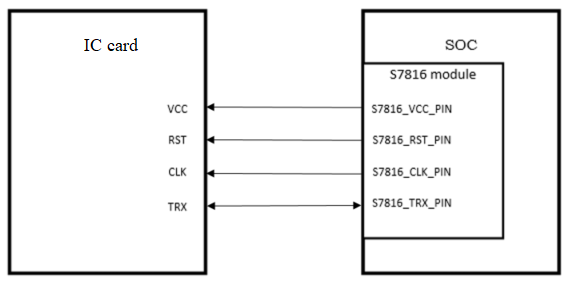
In actual use, we need to connect each contact of the IC card to the SoC one by one. This is the hardware foundation for communication between the SoC and the IC card.
- VCC is the power supply voltage of the IC card, and RST is the reset signal of the IC card. Any two free GPIO pins of the SoC can be chosen to connect to them.
- CLK is the clock contact of the IC card. The SoC supplies the clock to the IC card.
- TRX, i.e., the I/O contact, is the input/output contact of the IC card. Since the IC card only supports half-duplex communication, the I/O contact only supports input or output at any given moment, so the timing needs to be paid attention to in actual use.
Note
ISO/IEC 7816-3 specifies three operating voltages for IC cards: Class A - 5V, Class B - 3V, Class C - 1.8V. In actual use, the voltage provided by the SoC must match the operating voltage of the card.
Initialization
s7816_set_pin(gpio_pin_e rst_pin,gpio_pin_e vcc_pin,gpio_pin_e clk_pin,gpio_pin_e trx_pin)
s7816_init(uart_num_e uart_num,s7816_clock_e clock,int f,int d)
s7816_set_pin()is used to configure the RST, VCC, CLK, and TRX pins.s7816_init()is used to select the UART channel (UART0 and UART1), configure the IC card clock, and configure the IC card clock rate conversion factor F (default 372) and baud rate adjustment factor D (default 1). F, D, and the CLK clock frequency jointly determine the elementary time unit etu, i.e., 1 etu = (F/D) × (1/f). See Elementary Time Unit (etu) and Rate Factors F/D.
s7816_en(uart_num_e chn)
After the configuration is complete, use the function s7816_en() to enable the 7816 module.
Note
s7816 is implemented through the SoC's UART function, so it occupies the corresponding UART module when in use.
IC Card Activation and Cold Reset
s7816_coldreset();
ISO/IEC 7816-3 specifies that after the reset pin is pulled high (Tb), the cold reset answer (ATR) will start within the following 400~40000 clock cycles.
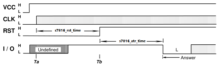
Taking an SoC clock configuration of 4 MHz as an example, the cold reset process is as follows:
- Activation: First set RST to low level, then pull up VCC to supply power, then configure the SoC's TRX pin to the receiving state, and finally output CLK to the IC card at time Ta.
- Within 200 clock cycles after Ta, the IC card will set I/O to high level, indicating that it has entered the reception-ready state.
- According to the standard, after CLK is applied, RST must remain low for at least 400 clock cycles, and then be pulled high at time Tb. The driver's default
s7816_rst_timewaiting time is 40000 clock cycles (10000 us at 4 MHz), i.e., the SoC waits at most 40000 clock cycles after Ta before pulling RST high. This waiting time can be reconfigured usings7816_set_time(). - Within 400~40000 clock cycles after Tb (RST pulled high) (corresponding to 100 us~10000 us at 4 MHz), the IC card will transmit the reset characters (ATR) to the SoC. If there is no response within 40000 clock cycles, the terminal should perform contact release (deactivation).
s7816_set_time(int rst_time_us)
s7816_set_time() is used to reconfigure the s7816_rst_time in the cold reset.
rst_time_uscorresponds tos7816_rst_time, which is the reset waiting time from Ta to Tb in the sequence. The default is 40000 clock cycles.s7816_atr_timeis the time to wait for the ATR after Tb in the sequence. According to the standard, its range is uncertain at 400~40000 clock cycles. In actual use, you need to wait until the ATR characters have been completely received before proceeding to the next step (you can parse the protocol in the main function to determine whether the ATR characters have been completely received).
Hot Reset
s7816_warmreset()

The IC card has specified specifications and contents for the reset answer to the terminal (SoC). If the reset answer received by the terminal does not meet the specified requirements, the terminal will initiate a hot reset and obtain a reset signal from the IC card.
Taking a clock configuration of 4 MHz as an example, the hot reset process is as follows:
- CLK and VCC always remain in the normal state (CLK applied, VCC pulled up).
- At time Tc, set RST from high to low.
- Within 200 clock cycles after Tc (50 us), the SoC sets the TRX pin to the receiving state (the standard requires the IC card to set I/O to high level within 200 clock cycles after Tc).
- According to the standard, RST must remain low for at least 400 clock cycles; the driver waits at most 40000 clock cycles by default (10000 us at 4 MHz), and then pulls RST high at time Td. The IC card's reset answer will start within 400~40000 clock cycles after Td (corresponding to 100 us~10000 us at 4 MHz).
Same as the cold reset, the hot reset can also use the s7816_set_time() function to reconfigure s7816_rst_time (default 40000 clock cycles). You need to wait until the ATR characters have been completely received before proceeding to the next step.
Info
The reset answers (initial ATR) of the cold reset and hot reset are the same. The difference between the two is that the cold reset is accompanied by the activation of the IC card, while the hot reset is performed after the IC card has been activated.
Contact Release
s7816_release_trig()
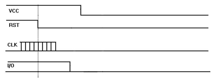
During a cold reset or hot reset, if the IC card does not give a reset answer within the specified time, the terminal needs to initiate a contact release sequence.
- The terminal starts the contact release sequence by setting RST to low level.
- After setting RST to low level and before powering off VCC, the terminal also sets CLK and I/O to low level.
- Finally, before actually disconnecting the contacts, the terminal powers off VCC.
Demo Introduction
The Demo takes an initialized SMARTCOS-PSAM card as an example. This card is a contact CPU card (PSAM card) compliant with the ISO/IEC 7816 standard, with a COS of SmartCOS V3.3 and using the T=0 protocol. The Demo first performs a cold reset, then gets a random number.
The get random number command is: 0x00,0x84,0x00,0x00,0x04 (get 4 bytes of random number). This is a standard command APDU:
- CLA=0x00 (ISO command class)
- INS=0x84 (GET CHALLENGE, get random number)
- P1=0x00, P2=0x00, Le=0x04 (expects 4 bytes of data to be returned)
Cold reset to obtain the initial ATR:

The initial ATR has a total of 16 bytes. The analysis of the initial ATR is as follows:
- 3B: Direct convention.
- 6C: This is T0. The binary of the high nibble 6 is 0110, indicating that TB1 and TC1 are present; the low nibble C indicates that there are 12 historical characters.
- From T0, it can be known that TB1 is 00, indicating that no extra programming voltage is needed.
- From T0, it can be known that TC1 is 02, i.e., the extra guard time N=2. Under the T=0 protocol, when the terminal sends characters after receiving characters from the IC card, an additional 2 etu of guard time needs to be added on top of the standard 12 etu character interval.
- From T0, it can be known that the 12 historical characters are 0x58,0x02,0x86,0x38,0x50,0x53,0x41,0x4d,0x80,0x00,0x83,0x73 (where 0x50,0x53,0x41,0x4d is the ASCII code for "PSAM").
- There is no TD in the ATR, so the T=0 protocol is adopted by default, and therefore there is no TCK check character.
Get random number:

Among them, 0x00,0x84,0x00,0x00,0x04 is the get random number command sent by the terminal to the IC card.
The random number obtained is 0xf0,0x44,0xef,0x7f, 4 bytes in total, and the random number obtained each time is different.
The trailing 9000 in the data indicates that the command was executed successfully (i.e., the status word SW1SW2 of the response APDU = 0x9000).
IR Learn
Overview
IR Learn is a peripheral for measuring the pulse width of infrared signals: an internal counter automatically latches the count value at every level transition of the signal, yielding the high-level duration and the cycle duration of each pulse. Based on this, the software performs infrared protocol decoding and waveform learning.
- Receive (RX): the core function of this module, measuring the pulse width and period of the input signal.
- Transmit (TX): reuses the PWM module's IR DMA FIFO mode to output waveforms. Digital TX is implemented entirely by PWM (see the "PWM" chapter); analog TX requires this module to enable the analog transmit path (
ir_learn_tx_init()). The test descriptions of each chip's Demo cover TX usage.
Typical applications:
- IR learn remote controls: record the remote control waveform, store and forward it (RX learning + PWM transmission)
- Protocol decoding: decode infrared protocols such as NEC according to pulse width/cycle rules
- Edge detection: reuse the counter mode for GPIO edge detection (see the "Basic Type" of chapter Demo)
Chips with the IR Learn module are divided into three groups according to hardware capability, with features included level by level: Basic Type (digital TX/RX only) → Standard Type (adds analog TX/RX) → Enhanced Type (adds FIFO/DMA). The following sections give usage instructions for each of these three groups. Users only need to read the section for their own chip; see the table below for the mapping between specific chip models and groups. This is the only place in this chapter where chip models are maintained:
| Chip | Type | Digital mode | Analog mode | RX data reading | timeout configuration | Data storage format | Counting clock | Analog circuit sleep management | Edge detection reuse | rx_invert_en |
|---|---|---|---|---|---|---|---|---|---|---|
| B80 (TLSR820x and TLSR8373), B87 (TLSR827x and TLSR8355) | Basic | ✅ | ❌ | Interrupt on each edge, read data | Fixed enum levels | 24-bit only | System clock | — | ✅ | ❌ |
| TC321x, TC123x | Standard | ✅ | ✅ | Interrupt on each edge, read data | Fixed enum levels | 24-bit only | System clock | ✅ (must disable/re-enable) | ✅ | ❌ |
| TL721x, TL321x, TL322x, TL521x | Enhanced | ✅ | ✅ | FIFO batch read or DMA automatic transfer to memory | 24-bit arbitrary writable value | 16 / 24-bit selectable | pclk (no frequency division) | ✅ (must disable/re-enable) | ✅ | ✅ (set 1 for analog RX only, 0 for digital RX) |
Note
- Only the chips listed in the table above support the IR Learn function; chips not listed do not support it.
Counting Principle
The following content is independent of the specific chip model and describes hardware behavior common to all chips. Differences between chip groups are summarized in the tables below and are not repeated in the text.
Idle Level
| RX mode | What determines the idle level | What the software needs to do | Applicable chips |
|---|---|---|---|
| Digital mode | Internal pull-up/pull-down (idle low → configure pull-down, idle high → configure pull-up) | Configure pull-up/pull-down | All |
| Analog mode | The default level of the IR receiver module is high | No pin/pull-up configuration needed | Standard, Enhanced |
| Configuration item | Basic type | Standard type | Enhanced type |
|---|---|---|---|
rx_invert_en |
Not available | Not available | Available: analog RX must set it to 1 (inverted), digital RX sets it to 0 |
Counting Modes and Counting Process
cnt_mode has only two categories of operation: edge-triggered (starts counting when the start edge arrives) and count-on-enable (starts counting immediately after ir_learn_en()). Choose according to the usage scenario:
| Usage scenario | Idle level | cnt_mode | Counting start point | Applicable chips |
|---|---|---|---|---|
| IR TX/RX | Low | RISING_EDGE_START_CNT (recommended) |
First rising edge | Basic, Standard, Enhanced |
| High | FALLING_EDGE_START_CNT |
First falling edge | Basic, Standard, Enhanced | |
| GPIO edge detection | Low | IL_EN_LOW_STATUS_START_CNT |
Moment of ir_learn_en() |
Basic, Standard |
| High | IL_EN_HIGH_STATUS_START_CNT |
Moment of ir_learn_en() |
Basic, Standard |
| First-value handling | Applicable chips |
|---|---|
| Edge-triggered + idle low: the first start edge only starts counting without latching; only from the second edge onwards are the values real pulse widths | Basic, Standard, Enhanced |
| Edge-triggered + idle high: the first latched value is a cycle but only contains the low-level duration (not a complete cycle) and must be discarded | All |
| Count-on-enable: the first signal edge triggers an interrupt immediately without missing the first edge, suitable for edge detection. In the interrupt, only count/toggle IO without reading data; even if the first value is the idle duration, no special handling is needed | Basic, Standard |
For enhanced analog RX, rx_invert_en=1 inverts the idle-high to idle-low, so both digital/analog modes uniformly use RISING_EDGE_START_CNT |
Enhanced |
The working process of each mode is shown in the figures below (legend descriptions are in the notes below each figure):
Idle low (the signal stays low when idle, e.g. a digital pin configured with pull-down):
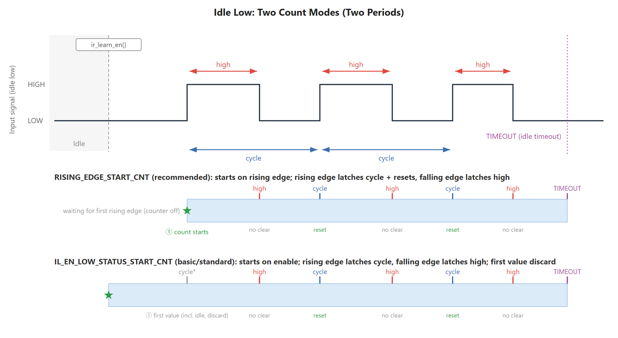
Idle high (the signal stays high when idle, e.g. an IR receiver head outputs high when there is no signal):
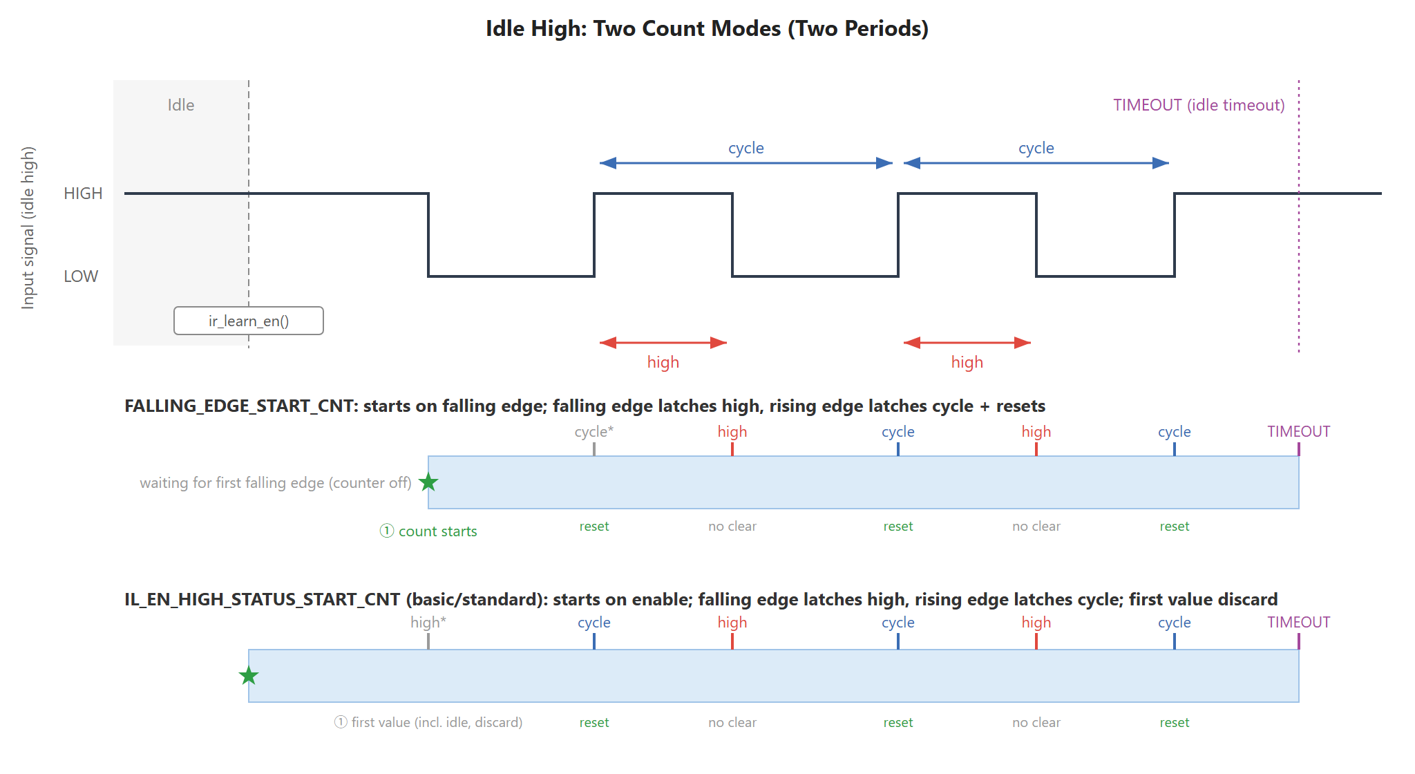
Mode selection conclusion: first determine the working mode according to the usage scenario, then select the corresponding mode according to the idle level. In digital mode, idle low → configure pull-down, idle high → configure pull-up; in analog mode the idle level is determined by hardware. If unsure, use the demo default RISING_EDGE_START_CNT + pull-down.
Note
- The A0 version of TC321x, and the A0/A1 versions of TL321x and TL721x chips miss the first edge during edge detection; configure the counting mode to falling-edge start to work around this.
Idle timeout: when the signal remains idle beyond the timeout threshold, a TIMEOUT interrupt is triggered and the counter stops, waiting for the next frame. In the enhanced FIFO mode, when the number of data bytes in the FIFO exceeds the set watermark, an RXFIFO interrupt is triggered (see the Enhanced Type chapter).
Count value precision: latched values contain an inherent quantization error of ±1 tick (related to the edge sampling moment). A difference of 1~2 ticks between the measured value and the real pulse width is normal; for precise calibration, measure with a known-width signal (send a signal of known pulse width and observe the latched values).
Counting Clock and Timeout
Counting clock: time(µs) = tick / clock frequency_MHz
| Item | Basic, Standard | Enhanced |
|---|---|---|
| Clock source | System clock | pclk (no frequency division) |
| Example | 16MHz → 1 tick = 62.5ns | 24MHz → 1 tick ≈ 41.7ns |
- The clock frequency directly determines the measurement resolution. When converting to time in software, the current actual running frequency must be used
- Do not change the system clock frequency during operation, otherwise data before and after is not comparable
TIMEOUT configuration: the threshold must be greater than the longest idle interval in the waveform (the low-level segment between bursts), otherwise the frame is mistakenly terminated midway and data is truncated.
| Item | Basic, Standard | Enhanced |
|---|---|---|
| timeout configuration | Fixed enum levels | 24-bit arbitrary writable value |
| Selection principle | Choose the smallest level greater than the longest interval | Directly write a value greater than the longest interval |
Basic Type
Digital mode only, using the legacy flat API (no struct), reading data via an interrupt on every transition edge. All code examples in this chapter use B80 chip as the example; the interface of B87 chip uses the same way.
Initialization
The following code uses B80 as an example:
ir_learn_set_pin(GPIO_PB5); // RX pin
gpio_setup_up_down_resistor(GPIO_PB5, PM_PIN_PULLDOWN_100K);
// pull-up/down follows cnt_mode: rising edge/low idle -> pull-down, falling edge/high idle -> pull-up
ir_learn_set_timeout(TICK_VALUE_65535); // timeout enum, choose a value larger than the longest low level
ir_learn_set_mode(RISING_EDGE_START_CNT); // count start mode
ir_learn_set_irq_mask(RISING_EDGE_IRQ | TIMEOUT_IRQ); // enable cycle + timeout interrupts
irq_set_mask(FLD_IRQ_IR_LEARN_EN); // enable IR Learn global interrupt
ir_learn_en(); // enable last after all config: edges before enable are not counted
Interrupts
| Interrupt | Trigger condition | Clear method |
|---|---|---|
RISING_EDGE_IRQ |
Rising edge detected, cycle value ready | Cleared manually by software |
FALLING_EDGE_IRQ |
Falling edge detected, high value ready | Cleared manually by software |
TIMEOUT_IRQ |
Counting exceeds the timeout threshold, frame ends | Cleared manually by software |
Use RISING_EDGE_IRQ as the main interrupt (when the cycle is ready, the high value is also ready and both can be read together); FALLING_EDGE_IRQ generally does not need to be enabled separately.
The following interrupt handling code uses B80 chip as an example:
if (ir_learn_get_irq_status(RISING_EDGE_IRQ)) {
ir_learn_clr_irq_status(RISING_EDGE_IRQ);
buf[idx++] = ir_learn_get_high(); // high level pulse width
buf[idx++] = ir_learn_get_cycle(); // cycle duration
}
if (ir_learn_get_irq_status(TIMEOUT_IRQ)) {
ir_learn_clr_irq_status(TIMEOUT_IRQ);
/* frame ends, process buf data */
}
On each rising-edge interrupt, a pair of values is read: high (high-level duration in ticks) and cycle (the complete cycle in ticks = high level + the adjacent low level). The waveform data of one frame is always stored in memory as [high, cycle, high, cycle, ...] in alternation.
Note
- Either clearing the interrupt before reading data or reading before clearing works (Standard/Enhanced types must read before clearing; see the corresponding chapters)
ir_learn_en()must be called last after all configuration is complete; edges arriving before enabling are not counted- In read-per-edge mode, the interrupt handling time must be shorter than the minimum edge interval (about 13µs for half the period of a 38kHz carrier), otherwise edges will be lost
Demo
(1) Hardware Connection
Single-board self-transmit and self-receive: connect the PWM pin to the RX pin (or via an IR emitter/receiver head) for self-testing. The following hardware connection uses B80 chip as an example:
| TX (PWM output) | RX (IR Learn input) |
|---|---|
| PC1 (PWM0) | PB5 |
Note
- If two boards are used for testing: connect the TX board's PWM pin to the RX board's PB5, with both boards sharing a common ground.
(2) Configuration Macros
The following configuration macros use the B80 Demo as an example:
##define IR_LEARN_MODE 1 // IR learn mode (self transmit and receive)
##define IR_LEARN_FOR_EDGE_DETECT_MODE 2 // edge detect mode
##define MODE_SELECT IR_LEARN_MODE // mode select
##define RISING_EDGE_CNT_MODE 0 // RISING_EDGE_START_CNT
##define HIGH_STATE_CNT_MODE 1 // IL_EN_HIGH_STATUS_START_CNT
##define FALLING_EDGE_CNT_MODE 2 // FALLING_EDGE_START_CNT
##define LOW_STATE_CNT_MODE 3 // IL_EN_LOW_STATUS_START_CNT
##define IRLEARN_CNT_MODE RISING_EDGE_CNT_MODE // count mode select
// edge detect mode only
##define RISING_EDGE 1
##define FALLING_EDGE 2
##define GPIO_IRQ_TYPE FALLING_EDGE // select rising/falling edge detect
(3) Test Description
The following test description is based on the B80 Demo (single-board self-transmit and self-receive).
IR learn mode (MODE_SELECT = IR_LEARN_MODE):
- Compile and flash the firmware to one board (single-board self-transmit and self-receive)
- TX uses the PWM IR DMA FIFO mode to send a preset waveform (
pwm_send_init()constructs the waveform data, filling tick values in the order [high, cycle, high, cycle, ...]), and a PWM interrupt is triggered when transmission completes - RX uses IR Learn per-edge interrupts to receive, storing data into
il_wave_receive_buff - After timeout, the frame ends; compare whether
il_wave_send_buff(sent data) andil_wave_receive_buff(received data) are consistent
Edge detection mode (MODE_SELECT = IR_LEARN_FOR_EDGE_DETECT_MODE):
- Compile and flash the firmware to one board
GPIO_IRQ_TYPEselects rising-edge or falling-edge detection- Rising-edge detection:
IL_EN_LOW_STATUS_START_CNT+ pull-down (the first rising edge triggers the interrupt immediately, without missing the first edge) - Falling-edge detection:
IL_EN_HIGH_STATUS_START_CNT+ pull-up (the first falling edge triggers the interrupt immediately, without missing the first edge) - In the interrupt, only count (
ir_rising_cnt/ir_falling_cnt) without reading high/cycle values
Test Results
| LED | Meaning |
|---|---|
| LED1 | Heartbeat (toggles every 500ms) |
| LED2 | Toggles once when TX transmission completes |
| LED3 | Toggles on RX edge interrupt / toggles in edge detection mode |
| LED4 | Toggles on RX timeout |
Set a breakpoint to view the il_wave_receive_buff variable and compare it with il_wave_send_buff to verify whether the transmitted and received data are consistent; in edge detection mode, check the ir_rising_cnt / ir_falling_cnt counters.
Note
- Edge detection reuse note: The Basic/Standard types support the "count-on-enable" mode (
IL_EN_LOW/HIGH_STATUS_START_CNT), where the first signal edge triggers an interrupt immediately without missing the first edge — closest to a true GPIO external interrupt. The Enhanced type does not have this mode and can only use edge triggering (the first edge only starts counting without triggering an interrupt, missing the first edge). With this usage on the Enhanced type, it is recommended to sethigh_data_en/cycle_data_ento 0 to avoid data accumulating in the FIFO.
Standard Type
Supports digital/analog modes, configured via the ir_learn_rx_t struct, reading data via an interrupt on every transition edge.
The differences between digital and analog modes are only two: change the rx_mode field to ANALOG_RX_MODE, and do not configure the RX pin in analog mode (the pin is internally connected directly to the analog circuit). The rest of the digital mode code is identical to analog.
Initialization
The following code uses TC321x as an example (TC123x is used the same way):
ir_learn_rx_t rx = {
.cnt_mode = RISING_EDGE_START_CNT,
.rx_mode = DIGITAL_RX_MODE, // change to ANALOG_RX_MODE for analog mode
.timeout_cnt = TICK_VALUE_65535,
};
ir_learn_rx_init(&rx);
ir_learn_set_dig_rx_pin(IR_RX_PA1, PM_PIN_PULLDOWN_100K);
// previous line is only needed for digital mode; delete it for analog mode
ir_learn_set_irq_mask(IR_LEARN_CYCLE_IRQ | IR_LEARN_TIMEOUT_IRQ | IR_LEARN_HIGH_IRQ);
irq_set_mask(FLD_IRQ_IR_LEARN_EN); // enable IR Learn global interrupt
ir_learn_en();
Interrupts
| Interrupt | Trigger condition | Clear method |
|---|---|---|
IR_LEARN_CYCLE_IRQ |
Rising edge detected, cycle value ready | Cleared manually by software |
IR_LEARN_HIGH_IRQ |
Falling edge detected, high value ready | Cleared manually by software |
IR_LEARN_TIMEOUT_IRQ |
Counting exceeds the timeout threshold, frame ends | Cleared manually by software (the driver internally performs disable→clear flag→enable to reset the module) |
Use IR_LEARN_CYCLE_IRQ as the main interrupt (when the cycle is ready, the high value is also ready). Read the data before clearing the interrupt; in the timeout handler, you must additionally check HIGH to take the last value. The following interrupt handling code uses TC321X as an example:
if (ir_learn_get_irq_status(IR_LEARN_CYCLE_IRQ)) {
buf[idx++] = ir_learn_get_high();
buf[idx++] = ir_learn_get_cycle();
ir_learn_clr_irq_status(IR_LEARN_CYCLE_IRQ);
ir_learn_clr_irq_status(IR_LEARN_HIGH_IRQ);
}
if (ir_learn_get_irq_status(IR_LEARN_TIMEOUT_IRQ)) {
// the last high value is still held at timeout, must be read out
if (ir_learn_get_irq_status(IR_LEARN_HIGH_IRQ)) {
buf[idx++] = ir_learn_get_high();
ir_learn_clr_irq_status(IR_LEARN_HIGH_IRQ);
}
ir_learn_clr_irq_status(IR_LEARN_TIMEOUT_IRQ);
// internally auto disable->clear flags->enable, module reset to receive next frame, no manual handling needed
/* frame ends, process buf data */
}
Note
- Read the data before clearing the interrupt; reversing the order will read 0 or lose data.
- In the TIMEOUT interrupt, additionally check HIGH_IRQ: at timeout the high register still holds the last value, which will be lost if not taken out.
- When clearing TIMEOUT, the driver internally automatically performs disable→clear flags→enable; the module resets and directly receives the next frame, so the user does not need to handle it manually.
- Analog RX on A0 version chips may miss the first trigger edge; the workaround is to change
cnt_modetoFALLING_EDGE_START_CNT(the demo checksg_chip_version == CHIP_VERSION_A0). - In read-per-edge mode, the interrupt handling time must be shorter than the minimum edge interval (about 13µs for half the period of a 38kHz carrier), otherwise edges will be lost.
Demo
(1) Hardware Connection
TC321x is used as an example here. Two-board test: compile one board in TX mode and the other in RX mode, connect TX/RX and share a common ground; or point the RX board at any remote control and press a key.
| TX board | RX board |
|---|---|
| PC0 | PA1 |
| GND | GND |
Note
- You can also skip the TX board and simply point any IR remote control at the RX board and press a key.
(2) Configuration Macros
The following configuration macros use the TC321x Demo as an example:
##define IR_DIGITAL_TX_MODE 0 // digital transmit
##define IR_DIGITAL_RX_MODE 1 // digital receive
##define IR_ANALOG_TX_MODE 2 // analog transmit
##define IR_ANALOG_RX_MODE 3 // analog receive
##define IR_LEARN_MODE IR_ANALOG_TX_MODE // choose one of four
##define IR_LEARN_PM_FUNCTION_EN 0 // sleep/wakeup function switch
(3) Test Description
The following test description is based on the TC321X Demo.
- Select the
IR_LEARN_MODEmacro to compile the corresponding mode (one of four: TX or RX) - TX mode:
pwm_send_init()constructs the waveform data (filling tick values in the order [high, cycle, high, cycle, ...]), transmitted in PWM IR DMA FIFO mode, with a PWM interrupt triggered when transmission completes; analog TX additionally callsir_learn_tx_init()to enable the analog transmit path - RX mode: initialize with
ir_learn_rx_init(), receive via per-edge interrupts, storing data intoil_wave_receive_buff - Analog RX mode: on A0 version chips, change
cnt_modetoFALLING_EDGE_START_CNT(the demo checksg_chip_version == CHIP_VERSION_A0) - Sleep/wakeup (
IR_LEARN_PM_FUNCTION_EN = 1): before entering suspend, analog RX callsir_learn_ana_rx_dis(); after wakeup, callsir_learn_ana_rx_en()
(4) Test Results
| LED | Meaning |
|---|---|
| LED1 | Heartbeat (toggles every 500ms) |
| LED2 | Toggles once when TX transmission completes |
| LED3 | Toggles on RX edge interrupt |
| LED4 | Toggles on RX timeout |
Set a breakpoint to view the il_wave_receive_buff variable and compare it with il_wave_send_buff to verify whether the transmitted and received data are consistent.
Enhanced Type
Supports digital/analog modes, uses the ir_learn_rx_t struct (with more fields), and reads data via the RX FIFO, supporting 16/24-bit storage formats.
The differences between digital and analog modes are only three: change rx_mode to ANALOG_RX_MODE, set rx_invert_en to 1 for analog, and do not configure the RX pin for analog. All code examples in this chapter use TL322x as the example; the interfaces of the other Enhanced-type chips are used the same way.
Data Format (16-bit / 24-bit)
The counter itself is fixed at 24 bits; "16-bit/24-bit" refers to the storage width when values are written into the FIFO (determined by the data_format field), not the counter width. The FIFO uses 32-bit words as storage units, and the two formats are packed differently:
| Storage format | Packing of a 32-bit FIFO word | Read method | Maximum representable value | Edges buffered per frame |
|---|---|---|---|---|
| 16-bit | Two 16-bit values packed into 1 word (e.g. [high, cycle] packed into 1 word) | ir_learn_get_data_by_hword() |
65,535 ticks (0xFFFF) | Doubled (saves half the FIFO space) |
| 24-bit | One 24-bit value zero-padded into 1 word | ir_learn_get_data_by_word() |
16,777,215 ticks (0xFFFFFF) | Fewer (fixed FIFO capacity, more bytes per value) |
How to choose: there is only one criterion — whether the largest cycle value in the waveform exceeds 65,535 ticks.
- The carrier period itself is short: one period at 38kHz is about 26µs ≈ 624 ticks (@24MHz), far below the limit.
- But the burst gap is counted into the next cycle: the NEC guide-code gap of 4.5ms ≈ 108,000 ticks (@24MHz), already exceeding the limit.
- Conclusion: for short-gap scenarios (gap < about 2.7ms @24MHz), 16-bit can be used, saving half the FIFO space; if there are long gaps or uncertainty, choose 24-bit directly — safe with no truncation.
Note
- The read API must match the
data_formatsetting: for the 16-bit format useby_hword()+ acnt/2loop; for the 24-bit format useby_word()+ acnt/4loop. Mixing them will misalign the data.
Initialization — FIFO Interrupt Method
The following code uses TL322x as an example:
ir_learn_rx_t rx = {
.high_data_en = 1,
.cycle_data_en = 1,
.timeout_en = 1,
.rx_invert_en = 0, // change to 1 for analog mode
.cnt_mode = RISING_EDGE_START_CNT,
.data_format = IR_LEARN_BIT_16_DATA, // change to IR_LEARN_BIT_24_DATA for 24-bit
.rx_mode = DIGITAL_RX_MODE, // change to ANALOG_RX_MODE for analog mode
};
ir_learn_rx_init(&rx);
ir_learn_set_dig_rx_pin(GPIO_PA0, GPIO_PIN_PULLDOWN_100K);
// previous line is only needed for digital mode; delete it for analog mode
ir_learn_rx_irq_trig_cnt(0x03); // interrupt triggered when FIFO byte count exceeds N (N is 0~7)
ir_learn_set_irq_mask(FLD_IR_LEARN_RXFIFO_IRQ | FLD_IR_LEARN_TIMEOUT_IRQ);
core_interrupt_enable();
plic_interrupt_enable(IRQ_IR_LEARN);
ir_learn_en();
Initialization — DMA Method
After ir_learn_rx_init(), replace the FIFO interrupt configuration with DMA configuration (do not call ir_learn_rx_irq_trig_cnt and the RXFIFO interrupt mask). The following code uses TL322x as an example:
// method 1: normal DMA, transfers to a specified buffer at once
ir_learn_receive_dma(DMA1, (unsigned int *)g_ir_dma_rx_buff, sizeof(g_ir_dma_rx_buff));
// method 2: chain Ping-Pong DMA, two buffers alternate for seamless reception (long waveform / continuous reception)
ir_learn_set_dma_chain_llp(DMA1, (unsigned char *)g_rec_buff0, sizeof(g_rec_buff0), &rx_dma_list[0]);
ir_learn_rx_dma_add_list_element(DMA1, &rx_dma_list[0], &rx_dma_list[1], (unsigned char *)g_rec_buff1, sizeof(g_rec_buff1));
ir_learn_rx_dma_add_list_element(DMA1, &rx_dma_list[1], &rx_dma_list[0], (unsigned char *)g_rec_buff0, sizeof(g_rec_buff0));
dma_chn_en(DMA1);
DMA buffers must be 4-byte aligned (__attribute__((aligned(4)))). For basic DMA configuration, see the "DMA" chapter.
Interrupts
In the FIFO method, data writing is done automatically by hardware. Enable FLD_IR_LEARN_RXFIFO_IRQ + FLD_IR_LEARN_TIMEOUT_IRQ; there is no need to enable the HIGH/CYCLE interrupts.
| Interrupt | Trigger condition | Clear method |
|---|---|---|
FLD_IR_LEARN_HIGH_IRQ |
Falling edge detected, high value ready (generally unused in FIFO mode) | Cleared manually by software |
FLD_IR_LEARN_CYCLE_IRQ |
Rising edge detected, cycle value ready (generally unused in FIFO mode) | Cleared manually by software |
FLD_IR_LEARN_TIMEOUT_IRQ |
Counting exceeds the timeout threshold, frame ends | Cleared manually by software (clearing also clears the FIFO automatically) |
FLD_IR_LEARN_RXFIFO_IRQ |
Data bytes in the FIFO exceed the set trigger watermark | Cleared manually by software |
Configuration field descriptions:
| Field | Function | Description |
|---|---|---|
high_data_en |
Write high value to FIFO | Can be set to 0 if only the cycle matters, halving FIFO usage (e.g. for NEC-like protocols that distinguish carriers by cycle) |
cycle_data_en |
Write cycle value to FIFO | Usually enabled |
timeout_en |
Enable timeout | Must be enabled to detect the end of a frame |
rx_invert_en |
Invert the IR input signal | Must be 1 for analog RX (the analog waveform is inverted as a whole when fed into the digital path); 0 for digital RX |
cnt_mode |
Counting start mode | The Enhanced type only supports RISING_EDGE_START_CNT / FALLING_EDGE_START_CNT |
data_format |
Data storage format | 16-bit → read with by_hword() + cnt/2 loop; 24-bit → use by_word() + cnt/4 |
rx_mode |
Digital/analog | Digital additionally requires calling ir_learn_set_dig_rx_pin(); analog does not |
FIFO interrupt method interrupt handling (the DMA method does not need to handle the RXFIFO interrupt; in chain mode, data is handled in the DMA transfer complete interrupt). The following interrupt handling code uses TL322x as an example:
if (ir_learn_get_irq_status(FLD_IR_LEARN_RXFIFO_IRQ)) {
u8 cnt = ir_learn_get_rx_fifo_status(FLD_IR_LEARN_FIFO_RX_CNT);
for (u8 i = 0; i < cnt / 2; i++) // change to cnt/4 with ir_learn_get_data_by_word() for 24-bit format
buf[idx++] = ir_learn_get_data_by_hword();
ir_learn_clr_irq_status(FLD_IR_LEARN_RXFIFO_IRQ);
}
if (ir_learn_get_irq_status(FLD_IR_LEARN_TIMEOUT_IRQ)) {
// read out remaining data in FIFO first, then process the frame
while (ir_learn_get_rx_fifo_status(FLD_IR_LEARN_FIFO_RX_CNT) > 0) {
buf[idx++] = ir_learn_get_data_by_hword(); // use by_word() for 24-bit format
}
ir_learn_clr_irq_status(FLD_IR_LEARN_TIMEOUT_IRQ); // clearing also clears FIFO automatically
/* frame ends, process buf data */
}
Note
- Read the data before clearing the interrupt (explicitly required by the header file); reversing the order will read 0 or lose data
- Clear FIFO before clearing TIMEOUT: when the timeout interrupt triggers, there may still be remaining data in the FIFO. Clearing TIMEOUT directly without reading it out will lose the data (clearing TIMEOUT automatically clears the FIFO)
- In the FIFO interrupt method, if interrupts are not serviced in time (main loop blocked for too long, or interrupt handling takes too long), the FIFO will overflow and lose data. For long waveforms / continuous reception scenarios, switch to the DMA method, or increase the
ir_learn_rx_irq_trig_cnttrigger watermark - The DMA method does not need to handle the RXFIFO interrupt; in chain Ping-Pong mode, data is handled in the DMA transfer complete interrupt
- Analog RX on A0 version chips may miss the first trigger edge; use the FALLING_EDGE_START_CNT mode to work around it.
Demo
(1) Hardware Connection
Two-board test: the TX board transmits and the RX board receives, with a common ground. The following hardware connection uses TL322x as an example:
| TX board | RX board |
|---|---|
| PB3 | PA0 |
| GND | GND |
(2) Configuration Macros
The following configuration macros use the TL322x Demo as an example:
##define IR_DIGITAL_TX_MODE 0
##define IR_DIGITAL_RX_MODE 1
##define IR_ANALOG_TX_MODE 2
##define IR_ANALOG_RX_MODE 3
##define IR_LEARN_MODE IR_ANALOG_RX_MODE // choose one of four
// RX mode only
##define DMA_EN 0 // DMA switch (0=FIFO interrupt, 1=DMA)
##define DMA_LLP_PINGPONG 1
##define DMA_MODE_NO_CHAIN 2
##define DMA_MODE DMA_LLP_PINGPONG // DMA mode select
##define IR_LEARN_RX_DATA_WIDTH 16 // 16 or 24
(3) Test Description
The following test description is based on the TL322x Demo.
- Select the
IR_LEARN_MODEmacro to compile the corresponding mode (one of four: TX or RX) - TX mode:
pwm_send_init()constructs the waveform data (filling tick values in the order [high, cycle, high, cycle, ...]), transmitted in PWM IR DMA FIFO mode, with a PWM interrupt triggered when transmission completes; analog TX additionally callsir_learn_tx_init()to enable the analog transmit path - RX FIFO interrupt method (
DMA_EN = 0): the waveform received by IR Learn is written into the FIFO; the FIFO watermark triggers an interrupt, in which data is read out in batches and stored intog_il_wave_receive_buff - RX DMA method (
DMA_EN = 1): DMA automatically transfers FIFO data to a memory buffer; normal DMA or chain Ping-Pong dual buffers enable seamless reception - Compare
g_il_wave_send_buff(sent data) withg_il_wave_receive_buff(received data) to verify consistency
Test Results
| LED | Meaning |
|---|---|
| LED1 | Heartbeat (toggles every 500ms) |
| LED2 | Toggles once when TX transmission completes |
| LED3 | Toggles on RX timeout / toggles in the DMA transfer complete interrupt in chain DMA mode |
| LED4 | Toggles on RX FIFO interrupt (not triggered in DMA method) |
Set a breakpoint to view the g_il_wave_receive_buff variable and compare it with g_il_wave_send_buff to verify whether the transmitted and received data are consistent.
Note
- Before using analog mode, refer to the hardware schematic to connect the IR module power supply jumper.
Sleep Management [Analog Mode]
Analog RX/TX uses analog circuitry, which must be disabled before entering low power mode and re-enabled after wakeup (otherwise the analog circuitry still consumes power during sleep); digital mode has no analog circuitry and requires no handling for sleep/wakeup. Which source wakes the MCU is configured by the PM module (e.g. timer/external IO) and is unrelated to IR Learn.
| Timing | Operation |
|---|---|
| Before sleep | ir_learn_ana_rx_dis() / ir_learn_ana_tx_dis() |
| After wakeup | ir_learn_ana_rx_en() / ir_learn_ana_tx_en() |
After wakeup from suspend, register configurations are retained and no re-initialization is needed; after wakeup from deep and deep-retention sleep, re-initialization is required. The following example of calls before/after sleep uses TC321X as an example (Enhanced-type chips are used the same way; see the IR_LEARN_PM_FUNCTION_EN section in the Demo):
// disable analog RX before suspend
ir_learn_ana_rx_dis();
cpu_sleep_wakeup(SUSPEND_MODE, PM_WAKEUP_TIMER, clock_time() + 500*CLOCK_16M_SYS_TIMER_CLK_1MS);
// re-enable analog RX after wakeup
ir_learn_ana_rx_en();
FAQ
Q1: No data received at all (receive buffer all 0s)?
Check in order: ① In digital mode, does the pull-up/pull-down match the counting mode (see "Counting Principle")? ② [Analog] Is rx_mode set to ANALOG_RX_MODE? [Enhanced] Is rx_invert_en set to 1? ③ Is ir_learn_en() called and the interrupt mask enabled? ④ Is the TX board actually transmitting (check whether LED2 on the TX board toggles)?
Q2: Only the first frame or the first edge is lost?
Check whether ir_learn_en() is called immediately after configuration is complete. If it is the analog RX first-edge miss on A0/A1 version chips, see the version notes in the corresponding chip chapter.
Q3: Data mismatch, received values too large or doubled? [Enhanced]
The read API does not match data_format (16-bit uses by_hword()+cnt/2, 24-bit uses by_word()+cnt/4). See "Data Format" in the "Enhanced Type" chapter.
Q4: The timeout interrupt keeps being triggerred?
The timeout threshold is smaller than the low-level duration of the waveform. Increase it (configuration method see "Counting Clock and Timeout").
Q5: A segment of data at the end of a long waveform is lost?
[Standard] The TIMEOUT handler misses the additional HIGH interrupt check; [Enhanced] the FIFO is not cleared before clearing timeout. For the correct implementation, see the interrupt handling in the corresponding chip chapter.
Q6: Digital mode works, but analog mode receives nothing? [Standard/Enhanced]
Check in order: is rx_mode changed to ANALOG_RX_MODE? [Enhanced] Is rx_invert_en set to 1? Was set_dig_rx_pin() called by mistake (not needed for analog)? Is it an A0/A1 version chip?
Q7: Can it transmit and receive at the same time?
- Digital mode: yes. The Basic-type demo is exactly single-board self-transmit and self-receive (TX uses PWM, RX uses IR Learn, no conflict between them).
- Analog mode: no. Standard IR learning technically does not support true simultaneous TX/RX: the physical layer of IR communication is naturally half-duplex, mainstream remote control protocols are one-way, and combined TX/RX modules themselves are time-multiplexed.
Q8: How to use IR Learn for pure edge detection?
See the edge detection mode in the "Basic Type" chapter Demo — Basic/Standard types use the count-on-enable mode (no first-edge miss); the Enhanced type uses the edge-triggered mode (first edge missed).
Q9: How far can IR communication reach?
The IR Learn module is responsible for measuring/generating waveform timing. The communication distance is mainly determined by the external hardware, though the chip's analog reception performance also has some influence:
- Transmit side: transmit power, emission angle, drive current and carrier duty cycle of the IR emitter
- Receive side: receiver sensitivity, center frequency matching and filtering performance of the IR receiver head
- Chip side: performance of the chip's built-in analog receive circuitry (the SDK optimizes the analog receive performance for some chip versions to improve the learning distance), but the SDK does not provide a public sensitivity adjustment interface — to adjust the distance, start with the external components
- Environmental factors: ambient light interference (sunlight/fluorescent lamps), occlusion, and TX/RX angle deviation
- Protocol factors: carrier frequency (usually 38kHz), code rate, encoding scheme
Under common configurations (ordinary emitter + standard 38kHz receiver head, indoors without strong direct light), the reliable communication distance is generally around 5~10 meters, but this is a hardware design parameter that this module cannot guarantee. To optimize the distance, consider: increasing the emitter drive current (do not exceed the specification), adding a concentrating cover to the emitter, choosing a high-sensitivity receiver head, reducing the code rate, and avoiding strong light sources.
The SDK driver handbook does not specify concrete communication distances, because the distance for the same chip can vary by several times to dozens of times with different IR components, and stating a fixed value would be misleading.